

CD40101BMS
December 1992
Features
• High Voltage Type (20V Rating)
• 100% Tested for Quiescent Current at 20V
• 5V, 10V and 15V Parametric Ratings
• Maximum Input Current of 1µA at 18V Over Full Pack-
age Temperature Range; 100nA at 18V and +25
• Noise Margin (Over Full Package/Temperature Range)
- 1V at VDD = 5V
- 2V at VDD = 10V
- 2.5V at VDD = 15V
• Standardized Symmetrical Output Characteristics
• Meets All Requirements of JEDEC Tentative Standard
No. 13B, “Standard Specifications for Description of
‘B’ Series CMOS Devices”
Description
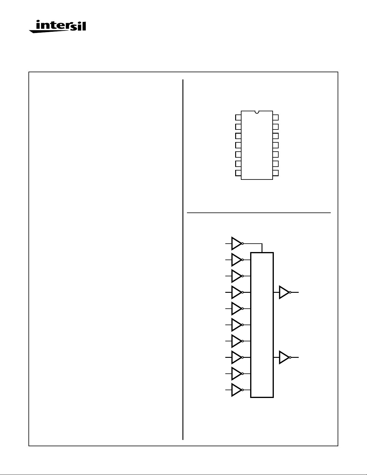
The CD40101BMS is a 9-bit (8 data bits plus 1 parity bit)
parity generator/checker. It may be used to detect errors in
data transmission or data retrieval. Odd and even outputs
facilitate odd or even parity generation and checking.
When used as a parity generator, a parity bit is supplied
along with the data to generate an even or odd parity output.
CMOS 9-Bit Parity Generator/Checker
Pinout
CD40101BMS
TOP VIEW
D1
1
D2
D3
D4
D9
VSS
2
3
4
5
6
7
o
C
ODD OUT
Functional Diagram
INHIBIT
8
D1 1
VDD
14
D8
13
D7
12
D6
11
D5
10
EVEN OUT
9
INHIBIT
8
VDD = 14
VSS = 7
When used as a parity checker, the received data bits and
parity bits are compared for correct parity. The even or odd
outputs are used to indicate an error in the received data.
Word length capability is expandable by cascading. The
CD40101BMS is also provided with an inhibit control. If the
inhibit control is set at logical “1”, the even and odd outputs
go to a logical “0”.
The CD40101BMS is supplied in these 14 lead outline
packages:
Braze Seal DIP H4H
Frit Seal DIP H1B
Ceramic Flatpack H3W
D2
D3
D4
D5
D6
D7
D8
D9
2
3
4
10
11
12
13
5
DECODE
EVEN
OUTPUT
9
ODD
OUTPUT
6
CAUTION: These devices are sensitive to electrostatic discharge; follow proper IC Handling Procedures.
1-888-INTERSIL or 321-724-7143 | Copyright © Intersil Corporation 1999
7-1286
File Number
3350
Specifications CD40101BMS
Absolute Maximum Ratings Reliability Information
DC Supply Voltage Range, (VDD) . . . . . . . . . . . . . . . -0.5V to +20V
(Voltage Referenced to VSS Terminals)
Input Voltage Range, All Inputs . . . . . . . . . . . . .-0.5V to VDD +0.5V
DC Input Current, Any One Input . . . . . . . . . . . . . . . . . . . . . . . .±10mA
Operating Temperature Range. . . . . . . . . . . . . . . . -55oC to +125oC
Package Types D, F, K, H
Storage Temperature Range (TSTG) . . . . . . . . . . . -65oC to +150oC
Lead Temperature (During Soldering) . . . . . . . . . . . . . . . . . +265oC
At Distance 1/16 ± 1/32 Inch (1.59mm ± 0.79mm) from case for
10s Maximum
TABLE 1. DC ELECTRICAL PERFORMANCE CHARACTERISTICS
PARAMETER SYMBOL CONDITIONS (NOTE 1)
Supply Current IDD VDD = 20V, VIN = VDD or GND 1 +25oC-10µA
VDD = 18V, VIN = VDD or GND 3 -55oC-10µA
Input Leakage Current IIL VIN = VDD or GND VDD = 20 1 +25oC -100 - nA
VDD = 18V 3 -55oC -100 - nA
Input Leakage Current IIH VIN = VDD or GND VDD = 20 1 +25oC - 100 nA
VDD = 18V 3 -55oC - 100 nA
Output Voltage VOL15 VDD = 15V, No Load 1, 2, 3 +25oC, +125oC, -55oC - 50 mV
Output Voltage VOH15 VDD = 15V, No Load (Note 3) 1, 2, 3 +25oC, +125oC, -55oC 14.95 - V
Output Current (Sink) IOL5 VDD = 5V, VOUT = 0.4V 1 +25oC 0.53 - mA
Output Current (Sink) IOL10 VDD = 10V, VOUT = 0.5V 1 +25oC 1.4 - mA
Output Current (Sink) IOL15 VDD = 15V, VOUT = 1.5V 1 +25oC 3.5 - mA
Output Current (Source) IOH5A VDD = 5V, VOUT = 4.6V 1 +25oC - -0.53 mA
Output Current (Source) IOH5B VDD = 5V, VOUT = 2.5V 1 +25oC - -1.8 mA
Output Current (Source) IOH10 VDD = 10V, VOUT = 9.5V 1 +25oC - -1.4 mA
Output Current (Source) IOH15 VDD = 15V, VOUT = 13.5V 1 +25oC - -3.5 mA
N Threshold Voltage VNTH VDD = 10V, ISS = -10µA 1 +25oC -2.8 -0.7 V
P Threshold Voltage VPTH VSS = 0V, IDD = 10µA 1 +25oC 0.7 2.8 V
Functional F VDD = 2.8V, VIN = VDD or GND 7 +25oC VOH >
VDD = 20V, VIN = VDD or GND 7 +25oC
VDD = 18V, VIN = VDD or GND 8A +125oC
VDD = 3V, VIN = VDD or GND 8B -55oC
Input Voltage Low
(Note 2)
Input Voltage High
(Note 2)
Input Voltage Low
(Note 2)
Input Voltage High
(Note 2)
NOTES: 1. All voltages referenced to device GND, 100% testing being
implemented.
2. Go/No Go test with limits applied to inputs.
VIL VDD = 5V, VOH > 4.5V, VOL < 0.5V 1, 2, 3 +25oC, +125oC, -55oC - 1.5 V
VIH VDD = 5V, VOH > 4.5V, VOL < 0.5V 1, 2, 3 +25oC, +125oC, -55oC 3.5 - V
VIL VDD = 15V, VOH > 13.5V,
VOL < 1.5V
VIH VDD = 15V, VOH > 13.5V,
VOL < 1.5V
Thermal Resistance . . . . . . . . . . . . . . . . θ
Ceramic DIP and FRIT Package. . . . . 80oC/W 20oC/W
Flatpack Package . . . . . . . . . . . . . . . . 70oC/W 20oC/W
Maximum Package Power Dissipation (PD) at +125oC
For TA = -55oC to +100oC (Package Type D, F, K) . . . . . . 500mW
For TA = +100oC to +125oC (Package Type D, F, K). . . . . .Derate
Linearity at 12mW/oC to 200mW
Device Dissipation per Output Transistor . . . . . . . . . . . . . . . 100mW
For TA = Full Package Temperature Range (All Package Types)
Junction Temperature . . . . . . . . . . . . . . . . . . . . . . . . . . . . . . +175oC
GROUP A
SUBGROUPS TEMPERATURE
2 +125oC - 1000 µA
2 +125oC -1000 - nA
2 +125oC - 1000 nA
1, 2, 3 +25oC, +125oC, -55oC- 4 V
1, 2, 3 +25oC, +125oC, -55oC11 - V
3. For accuracy, voltage is measured differentially to VDD. Limit
is 0.050V max.
ja
LIMITS
VDD/2
VOL <
VDD/2
θ
jc
UNITSMIN MAX
V
7-1287
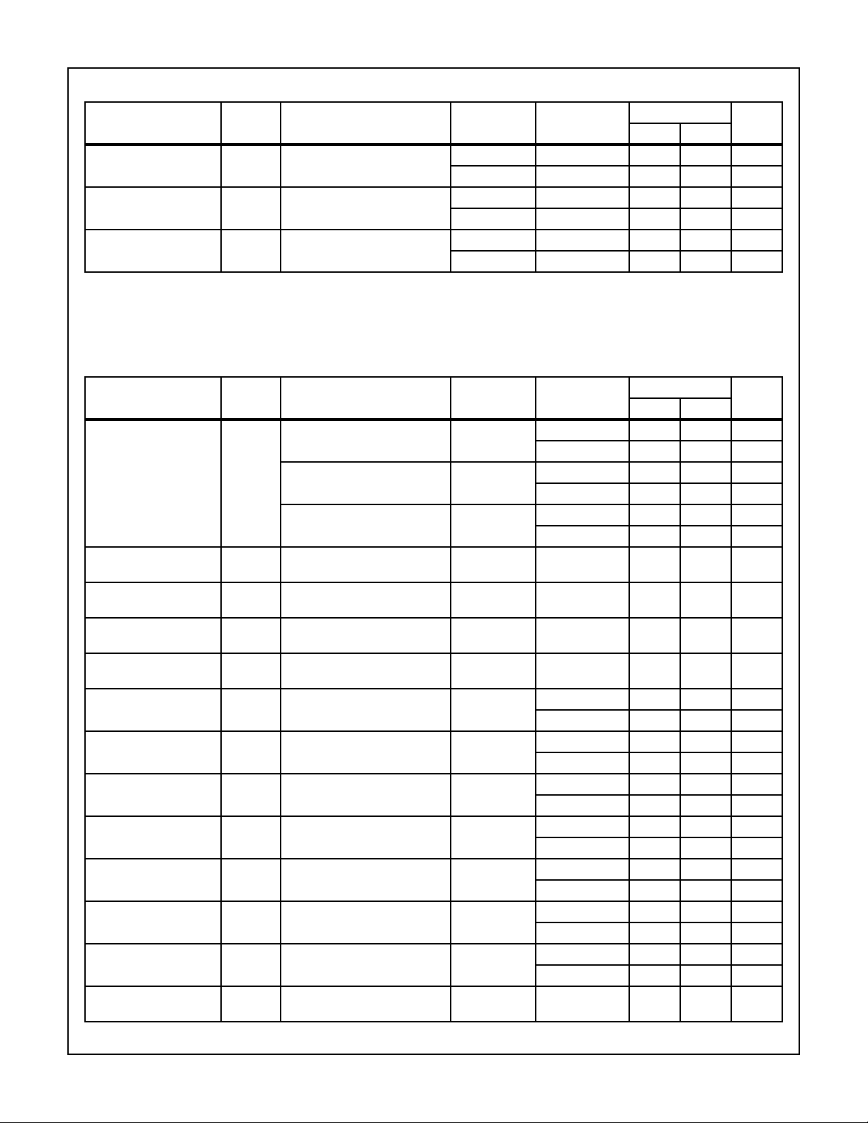
Specifications CD40101BMS
TABLE 2. AC ELECTRICAL PERFORMANCE CHARACTERISTICS
GROUP A
PARAMETER SYMBOL CONDITIONS (NOTE 1, 2)
Propagation Delay
Data-In To Output
Propagation Delay
Inhibit-In to Output
Transition Time TTHL
NOTES:
1. CL = 50pF, RL = 200K, Input TR, TF < 20ns.
2. -55oC and +125oC limits guaranteed, 100% testing being implemented.
PARAMETER SYMBOL CONDITIONS NOTES TEMPERATURE
Supply Current IDD VDD = 5V, VIN = VDD or GND 1, 2 -55oC, +25oC- 5 µA
Output Voltage VOL VDD = 5V, No Load 1, 2 +25oC, +125oC,
Output Voltage VOL VDD = 10V, No Load 1, 2 +25oC, +125oC,
Output Voltage VOH VDD = 5V, No Load 1, 2 +25oC, +125oC,
Output Voltage VOH VDD = 10V, No Load 1, 2 +25oC, +125oC,
Output Current (Sink) IOL5 VDD = 5V, VOUT = 0.4V 1, 2 +125oC 0.36 - mA
Output Current (Sink) IOL10 VDD = 10V, VOUT = 0.5V 1, 2 +125oC 0.9 - mA
Output Current (Sink) IOL15 VDD = 15V, VOUT = 1.5V 1, 2 +125oC 2.4 - mA
Output Current (Source) IOH5A VDD = 5V, VOUT = 4.6V 1, 2 +125oC - -0.36 mA
Output Current (Source) IOH5B VDD = 5V, VOUT = 2.5V 1, 2 +125oC - -1.15 mA
Output Current (Source) IOH10 VDD = 10V, VOUT = 9.5V 1, 2 +125oC - -0.9 mA
Output Current (Source) IOH15 VDD =15V, VOUT = 13.5V 1, 2 +125oC - -2.4 mA
Input Voltage Low VIL VDD = 10V, VOH > 9V, VOL <
TPHL1
TPLH1
TPHL2
TPLH2
TTLH
VDD = 5V, VIN = VDD or GND 9 +25oC - 700 ns
VDD = 5V, VIN = VDD or GND 9 +25oC - 280 ns
VDD = 5V, VIN = VDD or GND 9 +25oC - 200 ns
TABLE 3. ELECTRICAL PERFORMANCE CHARACTERISTICS
VDD = 10V, VIN = VDD or GND 1, 2 -55oC, +25oC- 10µA
VDD = 15V, VIN = VDD or GND 1, 2 -55oC, +25oC- 10µA
1V
SUBGROUPS TEMPERATURE
10, 11 +125oC, -55oC - 945 ns
10, 11 +125oC, -55oC - 378 ns
10, 11 +125oC, -55oC - 270 ns
+125oC - 150 µA
+125oC - 300 µA
+125oC - 600 µA
-55oC
-55oC
-55oC
-55oC
-55oC 0.64 - mA
-55oC 1.6 - mA
-55oC 4.2 - mA
-55oC - -0.64 mA
-55oC - -2.0 mA
-55oC - -1.6 mA
-55oC - -4.2 mA
1, 2 +25oC, +125oC,
-55oC
LIMITS
UNITSMIN MAX
LIMITS
UNITSMIN MAX
-50mV
-50mV
4.95 - V
9.95 - V
-3V
7-1288
Specifications CD40101BMS
TABLE 3. ELECTRICAL PERFORMANCE CHARACTERISTICS (Continued)
LIMITS
PARAMETER SYMBOL CONDITIONS NOTES TEMPERATURE
Input Voltage High VIH VDD = 10V, VOH > 9V, VOL < 1V 1, 2 +25oC, +125oC,
-55oC
Propagation Delay
Data to Output
Propagation Delay
Inhibit to Output
Transition Time TTLH
Input Capacitance CIN Any Input 1, 2 +25oC - 7.5 pF
NOTES:
1. All voltages referenced to device GND.
2. The parameters listed on Table 3 are controlled via design or process and are not directly tested. These parameters are characterized on
initial design release and upon design changes which would affect these characteristics.
3. CL = 50pF, RL = 200K, Input TR, TF < 20ns.
PARAMETER SYMBOL CONDITIONS NOTES TEMPERATURE
Supply Current IDD VDD = 20V, VIN = VDD or GND 1, 4 +25oC-25µA
N Threshold Voltage VNTH VDD = 10V, ISS = -10µA 1, 4 +25oC -2.8 -0.2 V
N Threshold Voltage
Delta
P Threshold Voltage VTP VSS = 0V, IDD = 10µA 1, 4 +25oC 0.2 2.8 V
P Threshold Voltage
Delta
Functional F VDD = 18V, VIN = VDD or GND 1 +25oC VOH >
Propagation Delay Time TPHL
NOTES: 1. All voltages referenced to device GND.
2. CL = 50pF, RL = 200K, Input TR, TF < 20ns.
TPHL1
TPLH1
TPHL2
TPLH2
TTHL
TABLE 4. POST IRRADIATION ELECTRICAL PERFORMANCE CHARACTERISTICS
∆VTN VDD = 10V, ISS = -10µA 1, 4 +25oC-±1V
∆VTP VSS = 0V, IDD = 10µA 1, 4 +25oC-±1V
TPLH
VDD = 10V 1, 2, 3 +25oC - 300 ns
VDD = 15V 1, 2, 3 +25oC - 200 ns
VDD = 10V 1, 2, 3 +25oC - 140 ns
VDD = 15V 1, 2, 3 +25oC - 100 ns
VDD = 10V 1, 2, 3 +25oC - 100 ns
VDD = 15V 1, 2, 3 +25oC - 80 ns
VDD = 3V, VIN = VDD or GND
VDD = 5V 1, 2, 3, 4 +25oC - 1.35 x
3. See Table 2 for +25oC limit.
4. Read and Record
7-V
LIMITS
VOL <
VDD/2
VDD/2
+25oC
Limit
UNITSMIN MAX
UNITSMIN MAX
V
ns
TABLE 5. BURN-IN AND LIFE TEST DELTA PARAMETERS +25oC
PARAMETER SYMBOL DELTA LIMIT
Supply Current - MSI-2 IDD ± 1.0µA
Output Current (Sink) IOL5 ± 20% x Pre-Test Reading
Output Current (Source) IOH5A ± 20% x Pre-Test Reading
TABLE 6. APPLICABLE SUBGROUPS
MIL-STD-883
CONFORMANCE GROUP
Initial Test (Pre Burn-In) 100% 5004 1, 7, 9 IDD, IOL5, IOH5A
Interim Test 1 (Post Burn-In) 100% 5004 1, 7, 9 IDD, IOL5, IOH5A
METHOD GROUP A SUBGROUPS READ AND RECORD
7-1289

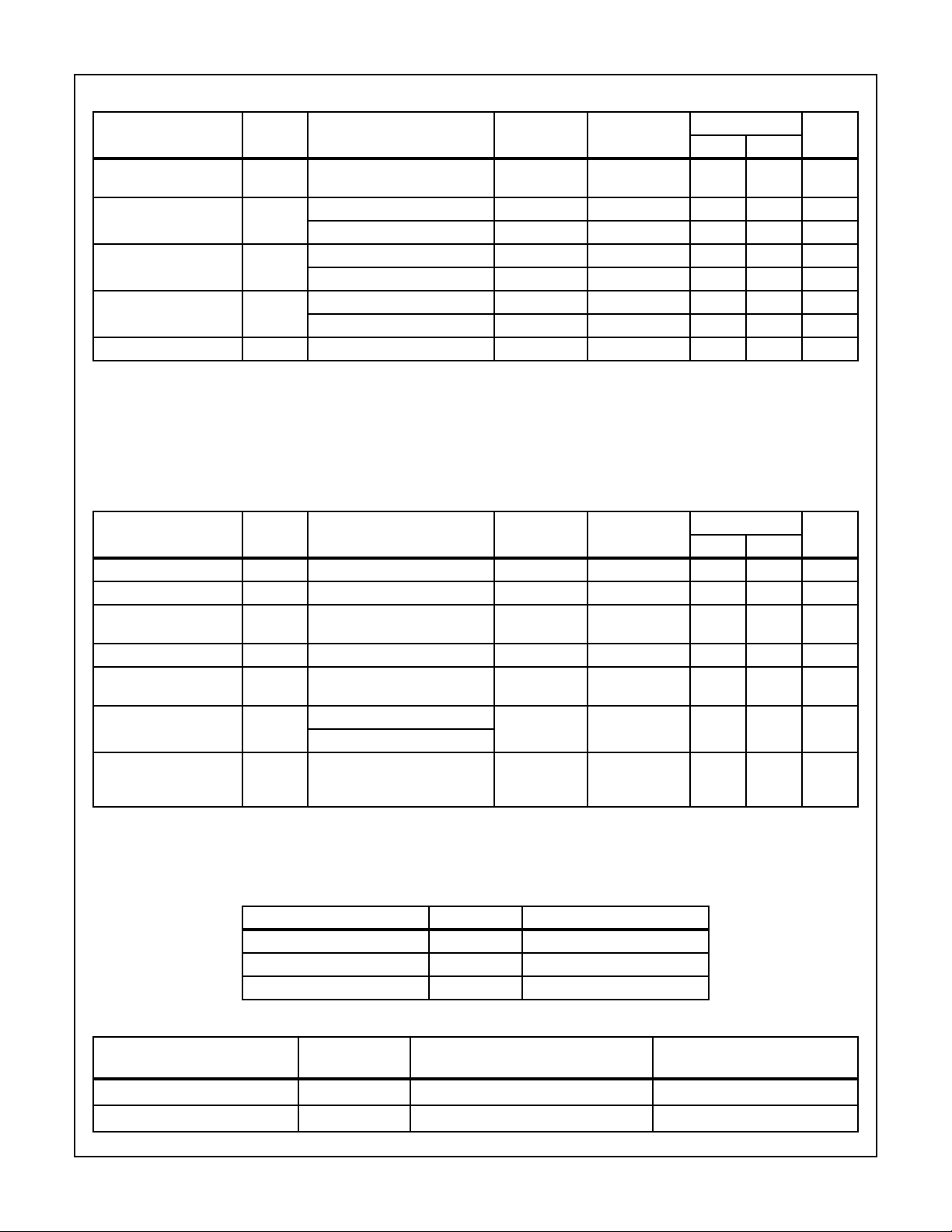
Specifications CD40101BMS
TABLE 6. APPLICABLE SUBGROUPS
MIL-STD-883
CONFORMANCE GROUP
Interim Test 2 (Post Burn-In) 100% 5004 1, 7, 9 IDD, IOL5, IOH5A
PDA (Note 1) 100% 5004 1, 7, 9, Deltas
Interim Test 3 (Post Burn-In) 100% 5004 1, 7, 9 IDD, IOL5, IOH5A
PDA (Note 1) 100% 5004 1, 7, 9, Deltas
Final Test 100% 5004 2, 3, 8A, 8B, 10, 11
Group A Sample 5005 1, 2, 3, 7, 8A, 8B, 9, 10, 11
Group B Subgroup B-5 Sample 5005 1, 2, 3, 7, 8A, 8B, 9, 10, 11, Deltas Subgroups 1, 2, 3, 9, 10, 11
Subgroup B-6 Sample 5005 1, 7, 9
Group D Sample 5005 1, 2, 3, 8A, 8B, 9 Subgroups 1, 2 3
NOTE: 1. 5% Parameteric, 3% Functional; Cumulative for Static 1 and 2.
CONFORMANCE GROUPS
Group E Subgroup 2 5005 1, 7, 9 Table 4 1, 9 Table 4
METHOD GROUP A SUBGROUPS READ AND RECORD
TABLE 7. TOTAL DOSE IRRADIATION
MIL-STD-883
METHOD
PRE-IRRAD POST-IRRAD PRE-IRRAD POST-IRRAD
TEST READ AND RECORD
TABLE 8. BURN-IN AND IRRADIATION TEST CONNECTIONS
OSCILLATOR
FUNCTION OPEN GROUND VDD 9V ± -0.5V
Static Burn-In 1
Note 1
Static Burn-In 2
Note 1
Dynamic BurnIn Note 1
Irradiation
Note 2
NOTES:
1. Each pin except VDD and GND will have a series resistor of 10K ± 5%, VDD = 18V ± 0.5V
2. Each pin except VDD and GND will have a series resistor of 47K ± 5%; Group E, Subgroup 2, sample size is 4 dice/wafer, 0 failures,
VDD = 10V ± 0.5V
6, 9 1-5, 7, 8, 10-13 14
6, 9 7 1-5, 8, 10-14
- 4, 7 12, 14 6, 9 2, 3, 5, 8, 10 1, 11, 13
6, 9 7 1-5, 8, 10-14
50kHz 25kHz
7-1290

Logic Diagram
1
D1
2
D2
3
D3
4
D4
10
D5
11
D6
12
D7
13
D8
5
D9
CD40101BMS
INHIBIT
8
VDD
EVEN
OUT
9
ODD
OUT
6
ALL INPUTS ARE PROTECTED
*
BY CMOS PROTECTION
NETWORK
VSS
TRUTH TABLE
INPUTS OUTPUTS
D1-D9 INHIBIT EVEN ODD
Σ1’s = Even 0 1 0
Σ1’s = Odd 0 0 1
X100
X = Don’t Care Logic 1 = High Logic 0 = Low
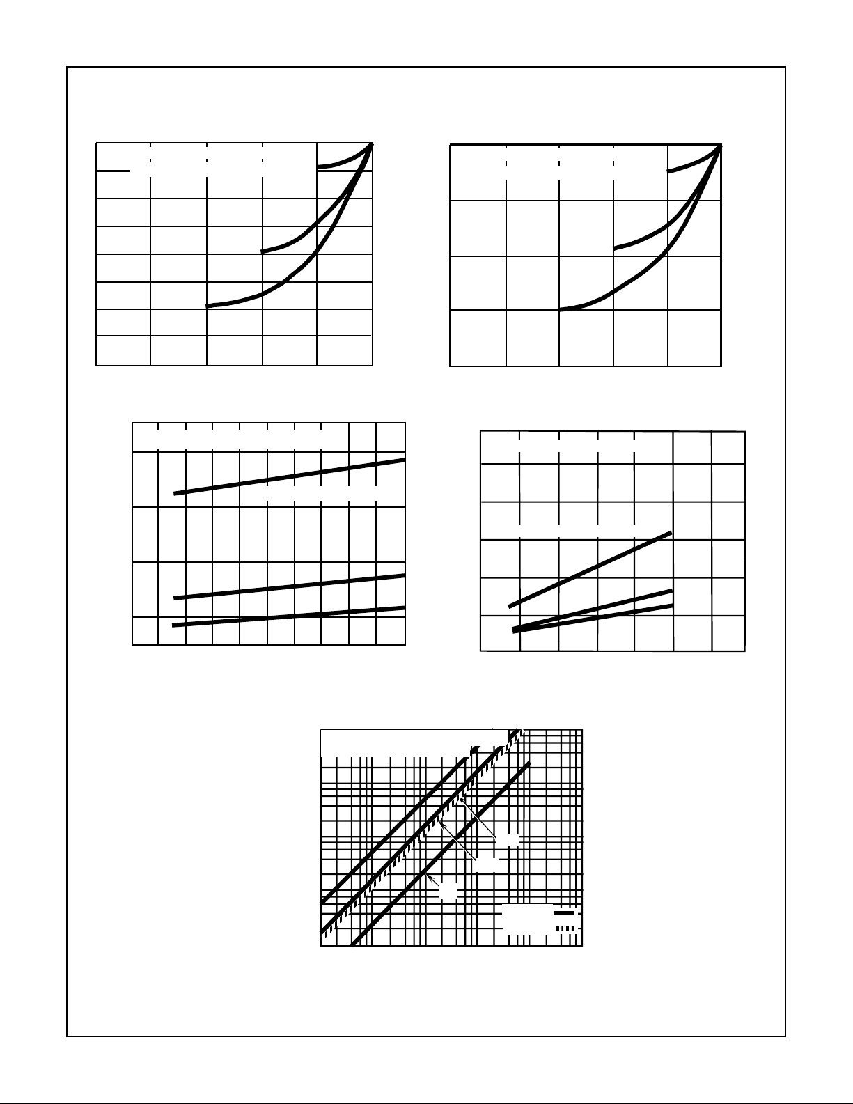
Typical Performance Characteristics
AMBIENT TEMPERATURE (TA) = +25oC
30
25
20
15
10
5
OUTPUT LOW (SINK) CURRENT (IOL) (mA)
0 5 10 15
FIGURE 2. TYPICAL OUTPUT LOW (SINK) CURRENT CHAR-
GATE-TO-SOURCE VOLTAGE (VGS) = 15V
10V
5V
DRAIN-TO-SOURCE VOLTAGE (VDS) (V)
ACTERISTICS
FIGURE 1.
AMBIENT TEMPERATURE (TA) = +25oC
15.0
12.5
10.0
7.5
5.0
2.5
OUTPUT LOW (SINK) CURRENT (IOL) (mA)
0 5 10 15
GATE-TO-SOURCE VOLTAGE (VGS) = 15V
10V
5V
DRAIN-TO-SOURCE VOLTAGE (VDS) (V)
FIGURE 3. MINIMUM OUTPUT LOW (SINK) CURRENT CHAR-
ACTERISTICS
7-1291
CD40101BMS
Typical Performance Characteristics (Continued)
DRAIN-TO-SOURCE VOLTAGE (VDS) (V)
0-5-10-15
AMBIENT TEMPERATURE (TA) = +25oC
GATE-TO-SOURCE VOLTAGE (VGS) = -5V
0
-5
-10
-15
-10V
-20
-25
-15V
-30
FIGURE 4. TYPICAL OUTPUT HIGH (SOURCE) CURRENT
CHARACTERISTICS
AMBIENT TEMPERATURE (TA) = +25oC
400
300
SUPPLY VOLTAGE (VDD) = 5V
DRAIN-TO-SOURCE VOLTAGE (VDS) (V)
AMBIENT TEMPERATURE (TA) = +25oC
GATE-TO-SOURCE VOLTAGE (VGS) = -5V
-10V
-15V
OUTPUT HIGH (SOURCE) CURRENT (IOH) (mA)
FIGURE 5. MINIMUM OUTPUT HIGH (SOURCE) CURRENT
CHARACTERISTICS
AMBIENT TEMPERATURE (TA) = +25oC
200
0-5-10-15
0
-5
-10
-15
OUTPUT HIGH (SOURCE) CURRENT (IOH) (mA)
200
10V
15V
100
PROPAGATION DELAY TIME (tPHL, tPLH) (ns)
50
0 20 40 60 80 100
10 30 50 70 90
LOAD CAPACITANCE (CL) (pF)
FIGURE 6. TYPICAL PROPAGATION DELAY TIME AS A
FUNCTION OF LOAD CAPACITANCE
AMBIENT TEMPERATURE (TA) = +25oC
4
10
8
SUPPLY VOLTAGE (VDD) = 15V
6
4
2
3
10
8
6
4
2
2
10
8
6
4
2
2
10
8
6
4
2
DYNAMIC POWER DISSIPATION (PD) (µW)
10
1
8642
10
INPUT FREQUENCY (fIN) (kHz)
150
SUPPLY VOLTAGE (VDD) = 5V
100
10V
50
TRANSITION TIME (tTHL, tTLH) (ns)
0
0 40 60 80 10020
15V
LOAD CAPACITANCE (CL) (pF)
FIGURE 7. TYPICAL TRANSITION TIME AS A FUNCTION OF
LOAD CAPACITANCE
10V
10V
5V
CL = 50pF
CL = 15pF
8642
10
8642
2
10
8642
3
10
8642
4
FIGURE 8. TYPICAL DYNAMIC POWER DISSIPATION AS A FUNCTION OF INPUT FREQUENCY
7-1292
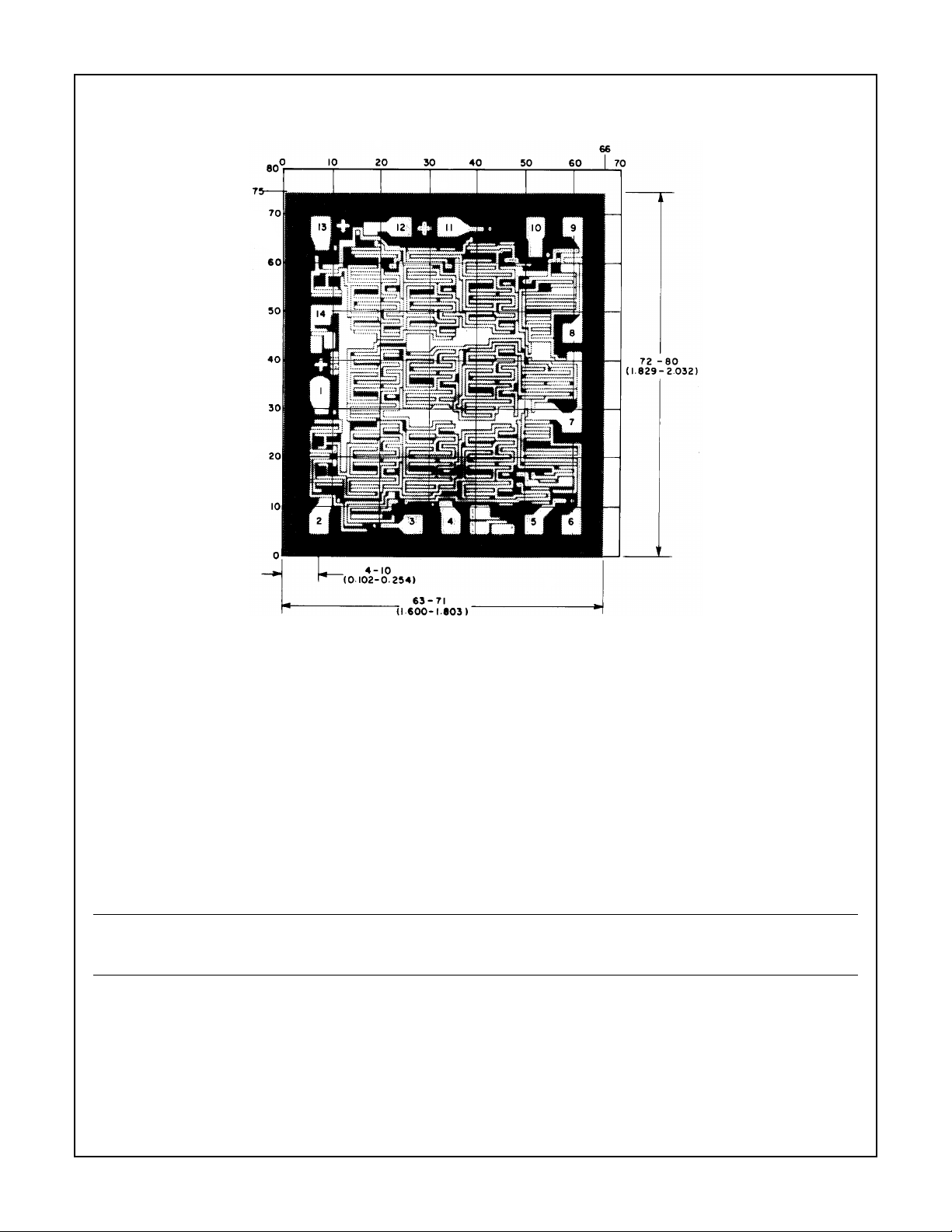
Chip Dimensions and Pad Layout
CD40101BMS
Dimensions in parenthesis are in millimeters and are
derived from the basic inch dimensions as indicated.
Grid graduations are in mils (10
-3
inch).
METALLIZATION: Thickness: 11kÅ − 14kÅ, AL.
PASSIVATION: 10.4kÅ - 15.6kÅ, Silane
BOND PADS: 0.004 inches X 0.004 inches MIN
DIE THICKNESS: 0.0198 inches - 0.0218 inches
All Intersil semiconductor products are manufactured, assembled and tested under ISO9000 quality systems certification.
Intersil products are sold by description only. Intersil Corporation reserves the right to make changes in circuit design and/or specifications at any time without
notice. Accordingly, the reader is cautioned to verify that data sheets are current before placing orders. Information furnished by Intersil is believed to be accurate
and reliable. However, no responsibility is assumed by Intersil or its subsidiaries for its use; nor for any infringements of patents or other rights of third parties which
may result from its use. No license is granted by implication or otherwise under any patent or patent rights of Intersil or its subsidiaries.
For information regarding Intersil Corporation and its products, see web site http://www.intersil.com
Sales Office Headquarters
NORTH AMERICA
Intersil Corporation
P. O. Box 883, Mail Stop 53-204
Melbourne, FL 32902
TEL: (321) 724-7000
FAX: (321) 724-7240
EUROPE
Intersil SA
Mercure Center
100, Rue de la Fusee
1130 Brussels, Belgium
TEL: (32) 2.724.2111
FAX: (32) 2.724.22.05
ASIA
Intersil (Taiwan) Ltd.
Taiwan Limited
7F-6, No. 101 Fu Hsing North Road
Taipei, Taiwan
Republic of China
TEL: (886) 2 2716 9310
FAX: (886) 2 2715 3029
1293
 Loading...