Intersil Corporation CD40100BMS Datasheet

December 1992
CD40100BMS
CMOS 32-Stage Static
Left/Right Shift Register
Features
• High Voltage Type (20V Rating)
• Fully Static Operation
• Shift Left/Shift Right Capability
• Multiple Package Cascading
• Recirculate Capability
• LIFO of FIFO Capability
• 100% Tested for Quiescent Current at 20V
• 5V, 10V and 15V Parametric Ratings
• Maximum Input Current of 1µA at 18V Over Full Pack-
age Temperature Range; 100nA at 18V and +25
o
C
• Noise Margin (Over Full Package/Temperature Range)
- 1V at VDD = 5V
- 2V at VDD = 10V
- 2.5V at VDD = 15V
• Standardized, Symmetrical Output Characteristics
• Meets All Requirements of JEDEC Tentative Standard
No. 13B, “Standard Specifications for Description of
‘B’ Series CMOS Devices”
Applications
• Serial Shift Registers
• Time Delay Circuits
• Expandable N-Bit Data Storage Stack (LIFO Operation)
Description
CD40100BMS is a 32-Stage shift register containing 32
D-type master-slave flip-flops.
The data present at the SHIFT RIGHT INPUT is transferred
into the first register stage synchronously with the positive
CLOCK edge, provided the LEFT/RIGHT CONTROL is at a
low level, the RECIRCULATE CONTROL is at a high level,
and the CLOCK INHIBIT is low. If the LEFT/RIGHT
CONTROL is at a high level and the RECIRCULATE
CONTROL is also high, data at the SHIFT LEFT INPUT is
transferred into the 32nd register stage synchronously with
the positive CLOCK transition, provided the CLOCK INHIBIT
is low. The state of the LEFT/RIGHT CONTROL,
RECIRCULATE CONTROL, and CLOCK INHIBIT should not
be changed when the CLOCK is high.
Data is shifted one stage left or one stage right depending on
the state of the LEFT/RIGHT CONTROL, synchronously with
the positive CLOCK edge. Data clocked into the first or 32nd
register states is available at the SHIFT LEFT or SHIFT
RIGHT OUTPUT respectively, on the next negative CLOCK
transition (see Data Transfer Table). No shifting occurs on the
positive CLOCK edge if the CLOCK INHIBIT line is at a high
level. With the RECIRCULATE CONTROL low, data in the
32nd stage is shifted into the first stage when the LEFT/
RIGHT CONTROL is low and from the first stage to the 32nd
stage when the LEFT/RIGHT CONTROL is low, and from the
first state to the 32nd stage when the LEFT/RIGHT control is
high. The CD40100BMS is supplied in these 16-lead outline
packages:
Braze Seal DIP H4T
Frit Seal DIP H2R
Ceramic Flatpack H6W
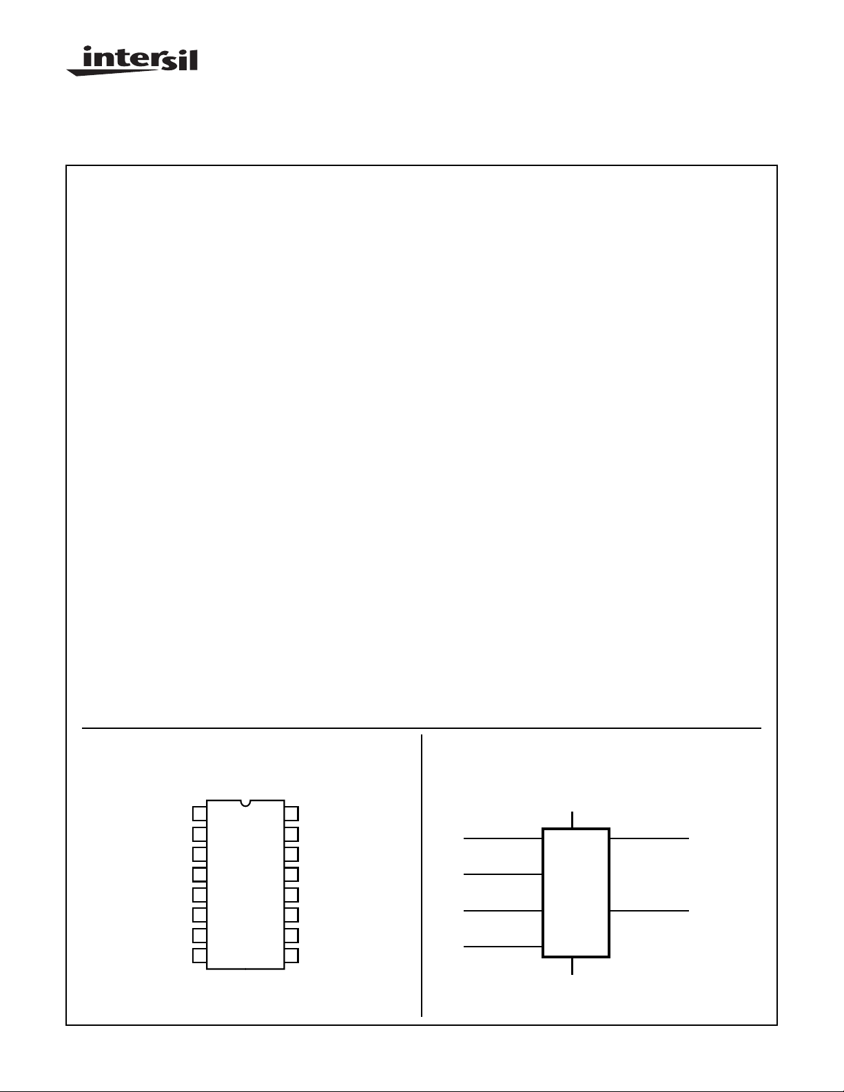
Pinout
CD40100BMS
TOP VIEW
16
1
NC
NC
NC
VSS
2
3
4
5
6
7
8
NC = NO CONNECTION
| Copyright © Intersil Corporation 1999
CLOCK INHIBIT
CLOCK
SHIFT LEFT OUT
SHIFT LEFT IN
CAUTION: These devices are sensitive to electrostatic discharge; follow proper IC Handling Procedures.
http://www.intersil.com or 407-727-9207
VDD
15
NC
14
NC
LEFT/RIGHT
13
CONTROL
12
SHIFT RIGHT OUT
11
SHIFT RIGHT IN
10
NC
RECIRCULATE
9
CONTROL
Functional Diagram
SHIFT RIGHT
IN
CLOCK INHIBIT
SHIFT LEFT
IN
7-1277
11
CLOCK
LEFT/RIGHT
CONTROL
13
4
2
6
9
RECIRCULATE
CONTROL
SHIFT RIGHT
12
SHIFT LEFT
4
VSS = 8
VDD = 16
NC = 1, 5, 7, 10, 14, 15
File Number
OUT
OUT
3349

Specifications CD40100BMS
Absolute Maximum Ratings Reliability Information
DC Supply Voltage Range, (VDD) . . . . . . . . . . . . . . . -0.5V to +20V
(Voltage Referenced to VSS Terminals)
Input Voltage Range, All Inputs . . . . . . . . . . . . .-0.5V to VDD +0.5V
DC Input Current, Any One Input . . . . . . . . . . . . . . . . . . . . . . . .±10mA
Operating Temperature Range. . . . . . . . . . . . . . . . -55oC to +125oC
Package Types D, F, K, H
Storage Temperature Range (TSTG). . . . . . . . . . . -65oC to +150oC
Lead Temperature (During Soldering) . . . . . . . . . . . . . . . . . +265oC
At Distance 1/16 ± 1/32 Inch (1.59mm ± 0.79mm) from case for
10s Maximum
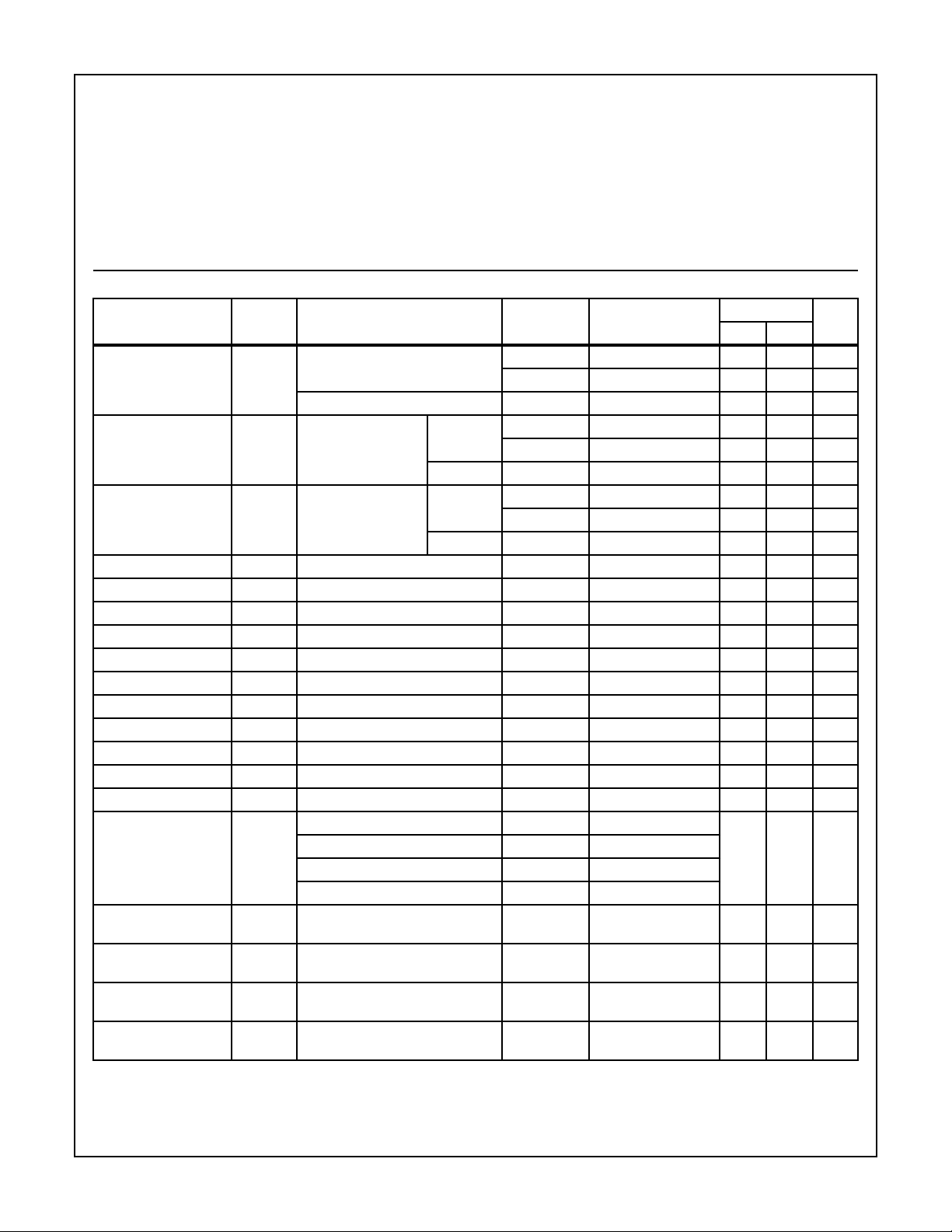
TABLE 1. DC ELECTRICAL PERFORMANCE CHARACTERISTICS
PARAMETER SYMBOL CONDITIONS (NOTE 1)
Supply Current IDD VDD = 20V, VIN = VDD or GND 1 +25oC-10µA
VDD = 18V, VIN = VDD or GND 3 -55oC-10µA
Input Leakage Current IIL VIN = VDD or GND VDD = 20 1 +25oC -100 - nA
VDD = 18V 3 -55oC -100 - nA
Input Leakage Current IIH VIN = VDD or GND VDD = 20 1 +25oC - 100 nA
VDD = 18V 3 -55oC - 100 nA
Output Voltage VOL15 VDD = 15V, No Load 1, 2, 3 +25oC, +125oC, -55oC - 50 mV
Output Voltage VOH15 VDD = 15V, No Load (Note 3) 1, 2, 3 +25oC, +125oC, -55oC 14.95 - V
Output Current (Sink) IOL5 VDD = 5V, VOUT = 0.4V 1 +25oC 0.53 - mA
Output Current (Sink) IOL10 VDD = 10V, VOUT = 0.5V 1 +25oC 1.4 - mA
Output Current (Sink) IOL15 VDD = 15V, VOUT = 1.5V 1 +25oC 3.5 - mA
Output Current (Source) IOH5A VDD = 5V, VOUT = 4.6V 1 +25oC - -0.53 mA
Output Current (Source) IOH5B VDD = 5V, VOUT = 2.5V 1 +25oC - -1.8 mA
Output Current (Source) IOH10 VDD = 10V, VOUT = 9.5V 1 +25oC - -1.4 mA
Output Current (Source) IOH15 VDD = 15V, VOUT = 13.5V 1 +25oC - -3.5 mA
N Threshold Voltage VNTH VDD = 10V, ISS = -10µA 1 +25oC -2.8 -0.7 V
P Threshold Voltage VPTH VSS = 0V, IDD = 10µA 1 +25oC 0.7 2.8 V
Functional F VDD = 2.8V, VIN = VDD or GND 7 +25oC VOH >
VDD = 20V, VIN = VDD or GND 7 +25oC
VDD = 18V, VIN = VDD or GND 8A +125oC
VDD = 3V, VIN = VDD or GND 8B -55oC
Input Voltage Low
(Note 2)
Input Voltage High
(Note 2)
Input Voltage Low
(Note 2)
Input Voltage High
(Note 2)
NOTES: 1. All voltages referenced to device GND, 100% testing being
implemented.
2. Go/No Go test with limits applied to inputs.
VIL VDD = 5V, VOH > 4.5V, VOL < 0.5V 1, 2, 3 +25oC, +125oC, -55oC - 1.5 V
VIH VDD = 5V, VOH > 4.5V, VOL < 0.5V 1, 2, 3 +25oC, +125oC, -55oC 3.5 - V
VIL VDD = 15V, VOH > 13.5V,
VOL < 1.5V
VIH VDD = 15V, VOH > 13.5V,
VOL < 1.5V
Thermal Resistance . . . . . . . . . . . . . . . . θ
Ceramic DIP and FRIT Package. . . . . 80oC/W 20oC/W
Flatpack Package . . . . . . . . . . . . . . . . 70oC/W 20oC/W
Maximum Package Power Dissipation (PD) at +125oC
For TA = -55oC to +100oC (Package Type D, F, K) . . . . . .500mW
For TA = +100oC to +125oC (Package Type D, F, K). . . . . .Derate
Linearity at 12mW/oC to 200mW
Device Dissipation per Output Transistor . . . . . . . . . . . . . . . 100mW
For TA = Full Package Temperature Range (All Package Types)
Junction Temperature . . . . . . . . . . . . . . . . . . . . . . . . . . . . . . +175oC
GROUP A
SUBGROUPS TEMPERATURE
2 +125oC - 1000 µA
2 +125oC -1000 - nA
2 +125oC - 1000 nA
1, 2, 3 +25oC, +125oC, -55oC- 4 V
1, 2, 3 +25oC, +125oC, -55oC11 - V
3. For accuracy, voltage is measured differentially to VDD. Limit
is 0.050V max.
ja
LIMITS
VDD/2
VOL <
VDD/2
θ
jc
UNITSMIN MAX
V
7-1278

Specifications CD40100BMS
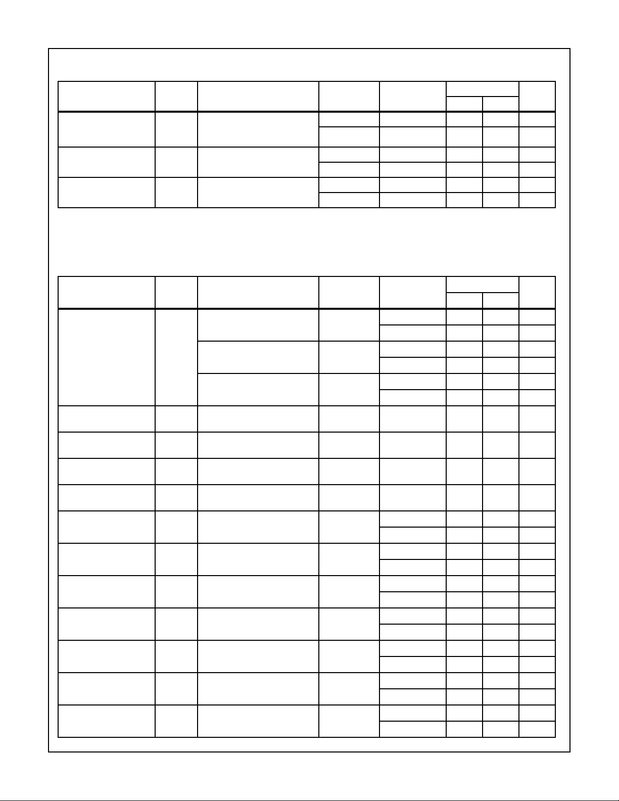
TABLE 2. AC ELECTRICAL PERFORMANCE CHARACTERISTICS
GROUP A
PARAMETER SYMBOL CONDITIONS (NOTE 1, 2)
Propagation Delay
Clock to Shift Left/Right
Output
Transition Time TTHL
Maximum Clock Input
Frequency
NOTES:
1. VDD = 5V, CL = 50pF, RL = 200K
2. -55oC and +125oC limits guaranteed, 100% testing being implemented.
PARAMETER SYMBOL CONDITIONS NOTES TEMPERATURE
Supply Current IDD VDD = 5V, VIN = VDD or GND 1, 2 -55oC, +25oC- 5 µA
Output Voltage VOL VDD = 5V, No Load 1, 2 +25oC, +125oC,
Output Voltage VOL VDD = 10V, No Load 1, 2 +25oC, +125oC,
Output Voltage VOH VDD = 5V, No Load 1, 2 +25oC, +125oC,
Output Voltage VOH VDD = 10V, No Load 1, 2 +25oC, +125oC,
Output Current (Sink) IOL5 VDD = 5V, VOUT = 0.4V 1, 2 +125oC 0.36 - mA
Output Current (Sink) IOL10 VDD = 10V, VOUT = 0.5V 1, 2 +125oC 0.9 - mA
Output Current (Sink) IOL15 VDD = 15V, VOUT = 1.5V 1, 2 +125oC 2.4 - mA
Output Current (Source) IOH5A VDD = 5V, VOUT = 4.6V 1, 2 +125oC - -0.36 mA
Output Current (Source) IOH5B VDD = 5V, VOUT = 2.5V 1, 2 +125oC - -1.15 mA
Output Current (Source) IOH10 VDD = 10V, VOUT = 9.5V 1, 2 +125oC - -0.9 mA
Output Current (Source) IOH15 VDD =15V, VOUT = 13.5V 1, 2 +125oC - -2.4 mA
TPHL
TPLH
TTLH
FCL VDD = 5V, VIN = VDD or GND 9 +25oC 1 - MHz
VDD = 5V, VIN = VDD or GND 9 +25oC - 720 ns
VDD = 5V, VIN = VDD or GND 9 +25oC - 200 ns
TABLE 3. ELECTRICAL PERFORMANCE CHARACTERISTICS
VDD = 10V, VIN = VDD or GND 1, 2 -55oC, +25oC- 10µA
VDD = 15V, VIN = VDD or GND 1, 2 -55oC, +25oC- 10µA
SUBGROUPS TEMPERATURE
10, 11 +125oC, -55oC - 972 ns
10, 11 +125oC, -55oC - 270 ns
10, 11 +125oC, -55oC .74 - MHz
+125oC - 150 µA
+125oC - 300 µA
+125oC - 600 µA
-55oC
-55oC
-55oC
-55oC
-55oC 0.64 - mA
-55oC 1.6 - mA
-55oC 4.2 - mA
-55oC - -0.64 mA
-55oC - -2.0 mA
-55oC - -1.6 mA
-55oC - -4.2 mA
LIMITS
UNITSMIN MAX
LIMITS
UNITSMIN MAX
-50mV
-50mV
4.95 - V
9.95 - V
7-1279
 Loading...