Intersil Corporation CD4008BMS Datasheet

November 1994
CD4008BMS
CMOS 4-Bit Full Adder With
Parallel Carry Out
Features
• High-Voltage Type (20V Rating)
• 4 Sum Outputs Plus Parallel Look-ahead Carry-Output
• High-Speed Operation - Sum In-To-Sum Out, 160ns
Typ; Carry In-To-Carry Out, 5ns Typ. At VDD = 10V,
CL=50pF
• Standardized Symmetrical Output Characteristics
• 100% Tested For Quiescent Current At 20V
• Maximum Input Current of 1µa at 18V Over Full Package-Temperature Range;
- 100nA at 18V and 25oC
• Noise Margin (Over Full Package T emperature Range):
- 1V at VDD = 5V
- 2V at VDD = 10V
- 2.5V at VDD = 15V
• 5V, 10V and 15V Parametric Ratings
• Meets All Requirements of JEDEC Tentative Standard
No. 13B, “Standard Specifications for Description of
‘B’ Series CMOS Devices”
Applications
• Binary Addition/Arithmetic Units
Description
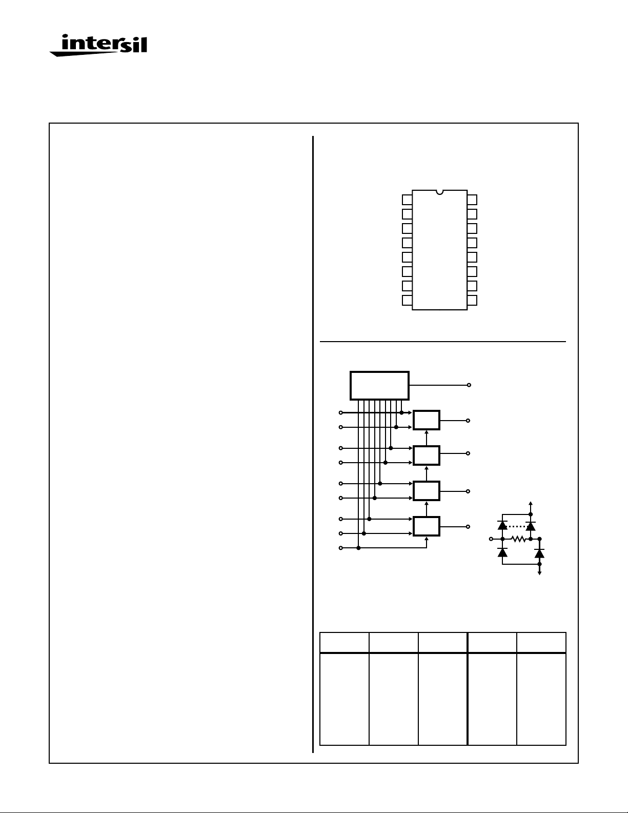
CD4008BMS types consist of four full adder stages with fast
look ahead carry provision from stage to stage. Circuitry is
included to provide a fast “parallel-carry-out” but to permit
high-speed operation in arithmetic sections using several
CD4008BMS’s.
CD4008BMS inputs include the four sets of bits to be added,
A1 to A4 and B1 to B4, in addition to the “Carry In” bit from a
previous section. CD4008BMS outputs include the four sum
bits, S1 to S4. In addition to the high speed “parallel-carryout” which may be utilized at a succeeding CD4008BMS
section.
The CD4008BMS is supplied in these 16-lead outline packages:
Braze Seal DIP H4T
Frit Seal DIP H1F
Ceramic Flatpack H6W
Pinout
A4
B3
A3
B2
A2
B1
A1
VSS
Logic Diagram
HIGH SPEED
PAR CARRY
15
*
B4
1
*
A4
2
*
B3
3
A3
*
4
*
B2
5
*
A2
6
*
B1
7
*
A1
9
*
C1
(CARRY-IN)
VDD = 16
VSS = 8
A
i
0
1
0
1
0
1
0
1
B
i
0
0
1
1
0
0
1
1
CD4008BMS
TOP VIEW
16
1
2
3
4
5
6
7
8
(CARRY-OUT)
SUM
C4
SUM
C3
SUM
C2
SUM
*ALL INPUTS ARE PROTECTED
BY CMOS PROTECTION
NETWORK
TRUTH TABLE
C
i
0
0
0
0
1
1
1
1
VDD
15
B4
14
CO
13
S4
12
S3
11
S2
10
S1
9
C1
14
CO
13
S4
12
S3
11
S2
10
S1
C
O
0
0
0
1
0
1
1
1
VDD
VSS
SUM
0
1
1
0
1
0
0
1
CAUTION: These devices are sensitive to electrostatic discharge; follow proper IC Handling Procedures.
1-888-INTERSIL or 321-724-7143 | Copyright © Intersil Corporation 1999
7-675
File Number
3292

Specifications CD4008BMS
Absolute Maximum Ratings Reliability Information
DC Supply Voltage Range, (VDD) . . . . . . . . . . . . . . . -0.5V to +20V
(Voltage Referenced to VSS Terminals)
Input Voltage Range, All Inputs . . . . . . . . . . . . .-0.5V to VDD +0.5V
DC Input Current, Any One Input . . . . . . . . . . . . . . . . . . . . . . . .±10mA
Operating Temperature Range. . . . . . . . . . . . . . . . -55
Package Types D, F, K, H
Storage Temperature Range (TSTG). . . . . . . . . . . -65
o
C to +125oC
o
C to +150oC
Lead Temperature (During Soldering) . . . . . . . . . . . . . . . . . +265
At Distance 1/16 ± 1/32 Inch (1.59mm ± 0.79mm) from case for
10s Maximum
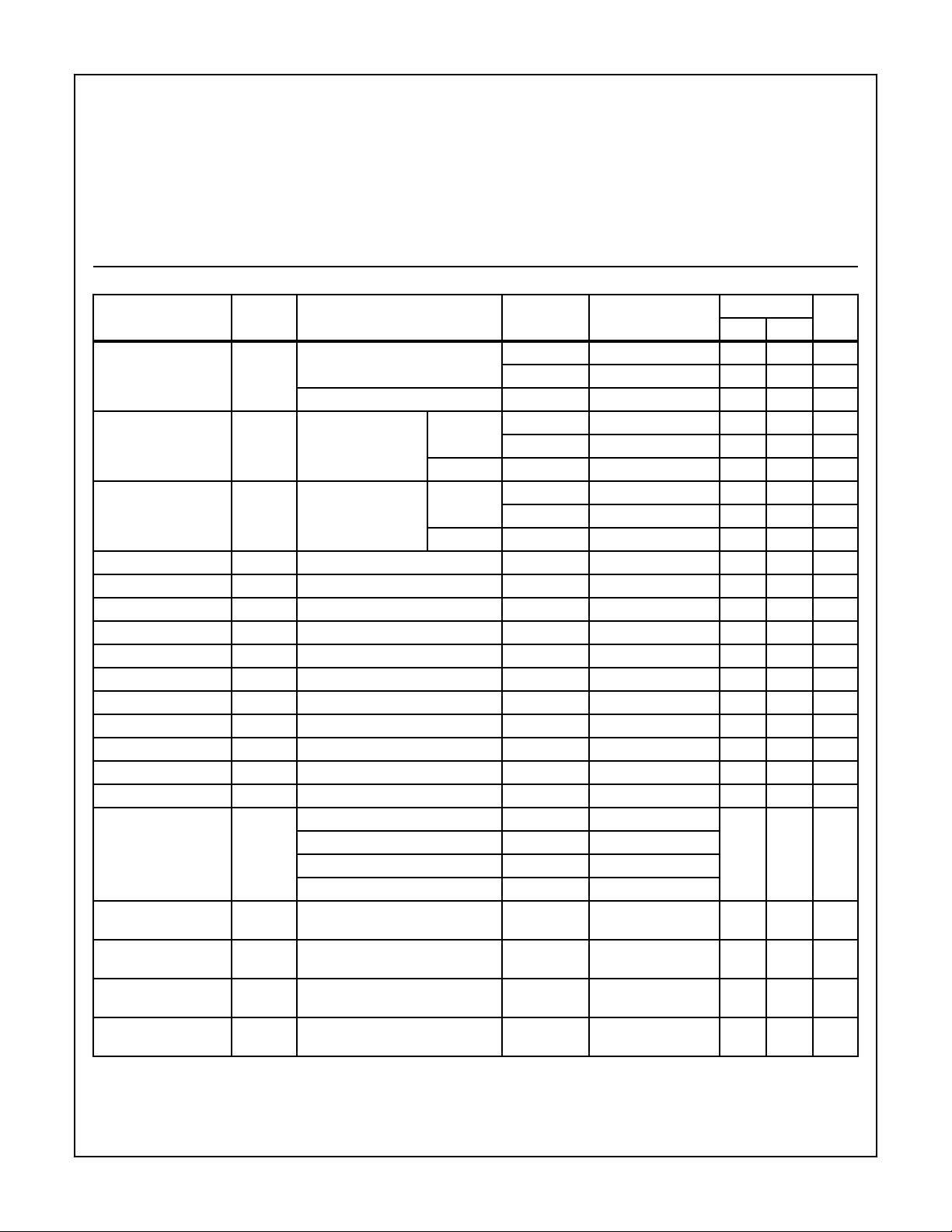
TABLE 1. DC ELECTRICAL PERFORMANCE CHARACTERISTICS
PARAMETER SYMBOL CONDITIONS (NOTE 1)
Supply Current IDD VDD = 20V, VIN = VDD or GND 1 +25
VDD = 18V, VIN = VDD or GND 3 -55oC-10µA
Input Leakage Current IIL VIN = VDD or GND VDD = 20 1 +25
VDD = 18V 3 -55oC -100 - nA
Input Leakage Current IIH VIN = VDD or GND VDD = 20 1 +25oC - 100 nA
VDD = 18V 3 -55oC - 100 nA
Output Voltage VOL15 VDD = 15V, No Load 1, 3 +25oC, +125oC, -55oC - 50 mV
Output Voltage VOH15 VDD = 15V, No Load (Note 3) 1, 3 +25oC, +125oC, -55oC 14.95 - V
Output Current (Sink) IOL5 VDD = 5V, VOUT = 0.4V 1 +25oC 0.53 - mA
Output Current (Sink) IOL10 VDD = 10V, VOUT = 0.5V 1 +25oC 1.4 - mA
Output Current (Sink) IOL15 VDD = 15V, VOUT = 1.5V 1 +25oC 3.5 - mA
Output Current (Source) IOH5A VDD = 5V, VOUT = 4.6V 1 +25oC - -0.53 mA
Output Current (Source) IOH5B VDD = 5V, VOUT = 2.5V 1 +25oC - -1.8 mA
Output Current (Source) IOH10 VDD = 10V, VOUT = 9.5V 1 +25oC - -1.4 mA
Output Current (Source) IOH15 VDD = 15V, VOUT = 13.5V 1 +25oC - -3.5 mA
N Threshold Voltage VNTH VDD = 10V, ISS = -10µA 1 +25oC -2.8 -0.7 V
P Threshold Voltage VPTH VSS = 0V, IDD = 10µA 1 +25oC 0.7 2.8 V
Functional F VDD = 2.8V, VIN = VDD or GND 7 +25oC VOH >
VDD = 20V, VIN = VDD or GND 7 +25oC
VDD = 18V, VIN = VDD or GND 8A +125oC
VDD = 3V, VIN = VDD or GND 8B -55oC
Input Voltage Low
VIL VDD = 5V, VOH > 4.5V, VOL < 0.5V 1, 2, 3 +25oC, +125oC, -55oC - 1.5 V
(Note 2)
Input Voltage High
VIH VDD = 5V, VOH > 4.5V, VOL < 0.5V 1, 2, 3 +25oC, +125oC, -55oC 3.5 - V
(Note 2)
Input Voltage Low
(Note 2)
Input Voltage High
(Note 2)
VIL VDD = 15V, VOH > 13.5V,
VOL < 1.5V
VIH VDD = 15V, VOH > 13.5V,
VOL < 1.5V
NOTES: 1. All voltages referenced to device GND, 100% testing being
implemented.
2. Go/No Go test with limits applied to inputs
Thermal Resistance . . . . . . . . . . . . . . . . θ
Ceramic DIP and FRIT Package. . . . . 80oC/W 20oC/W
Flatpack Package . . . . . . . . . . . . . . . . 70
Maximum Package Power Dissipation (PD) at +125oC
For TA = -55
For TA = +100
o
C
Device Dissipation per Output Transistor . . . . . . . . . . . . . . . 100mW
o
C to +100oC (Package Type D, F, K). . . . . .500mW
o
C to +125oC (Package Type D, F, K) . . . . .Derate
Linearity at 12mW/oC to 200mW
ja
o
C/W 20oC/W
For TA = Full Package Temperature Range (All Package Types)
Junction Temperature . . . . . . . . . . . . . . . . . . . . . . . . . . . . . . +175oC
GROUP A
LIMITS
SUBGROUPS TEMPERATURE
o
C-10µA
2 +125oC - 1000 µA
o
C -100 - nA
2 +125oC -1000 - nA
2 +125oC - 1000 nA
VOL <
VDD/2
VDD/2
1, 2, 3 +25oC, +125oC, -55oC- 4 V
1, 2, 3 +25oC, +125oC, -55oC11 - V
3. For accuracy, voltage is measured differentially to VDD. Limit
is 0.050V max.
θ
jc
UNITSMIN MAX
V
7-676

Specifications CD4008BMS
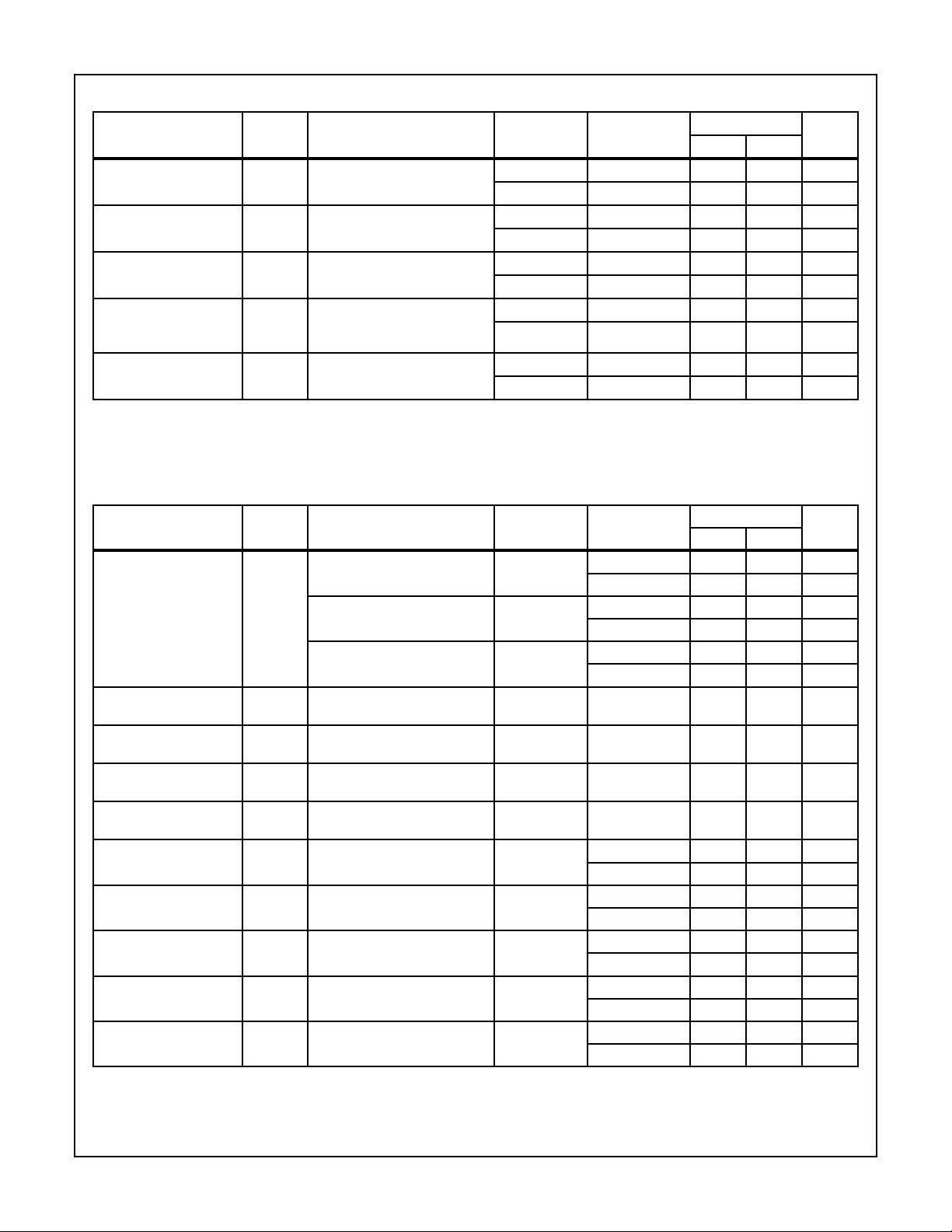
TABLE 2. AC ELECTRICAL PERFORMANCE CHARACTERISTICS
GROUP A
PARAMETER SYMBOL CONDITIONS (NOTE 1, 2)
Propagation Delay
Sum In to Sum Out
Propagation Delay
Carry In To Cum Out
Propagation Delay
Sum In To Carry Out
Propagation Delay
Carry In To
Carry Out
Transition Time TTHL
NOTES:
1. CL = 50pF, RL = 200K, Input TR, TF < 20ns.
2. -55oC and +125oC limits guaranteed, 100% testing being implemented.
PARAMETER SYMBOL CONDITIONS NOTES TEMPERATURE
Supply Current IDD VDD = 5V, VIN = VDD or GND 1, 2 -55oC, +25oC- 5 µA
Output Voltage VOL VDD = 5V, No Load 1, 2 +25oC, +125oC,
Output Voltage VOL VDD = 10V, No Load 1, 2 +25oC, +125oC,
Output Voltage VOH VDD = 5V, No Load 1, 2 +25oC, +125oC,
Output Voltage VOH VDD = 10V, No Load 1, 2 +25oC, +125oC,
Output Current (Sink) IOL5 VDD = 5V, VOUT = 0.4V 1, 2 +125oC 0.36 - mA
Output Current (Sink) IOL10 VDD = 10V, VOUT = 0.5V 1, 2 +125oC 0.9 - mA
Output Current (Sink) IOL15 VDD = 15V, VOUT = 1.5V 1, 2 +125oC 2.4 - mA
Output Current (Source) IOH5A VDD = 5V, VOUT = 4.6V 1, 2 +125oC - -0.36 mA
Output Current (Source) IOH5B VDD = 5V, VOUT = 2.5V 1, 2 +125oC - -1.15 mA
TPHL1
TPLH1
TPHL2
TPLH2
TPHL3
TPLH3
TPHL4
TPLH4
TTLH
VDD = 5V, VIN = VDD or GND 9 +25oC - 800 ns
VDD = 5V, VIN = VDD or GND 9 +25oC - 740 ns
VDD = 5V, VIN = VDD or GND 9 +25oC - 400 ns
VDD = 5V, VIN = VDD or GND 9 +25oC - 200 ns
VDD = 5V, VIN = VDD or GND 9 +25oC - 200 ns
TABLE 3. ELECTRICAL PERFORMANCE CHARACTERISTICS
VDD = 10V, VIN = VDD or GND 1, 2 -55oC, +25oC- 10µA
VDD = 15V, VIN = VDD or GND 1, 2 -55oC, +25oC- 10µA
SUBGROUPS TEMPERATURE
10, 11 +125oC, -55oC - 1080 ns
10, 11 +125oC, -55oC - 999 ns
10, 11 +125oC, -55oC - 540 ns
10, 11 +125oC, -55oC - 270 ns
10, 11 +125oC, -55oC - 270 ns
+125oC - 150 µA
+125oC - 300 µA
+125oC - 600 µA
-55oC
-55oC
-55oC
-55oC
-55oC 0.64 - mA
-55oC 1.6 - mA
-55oC 4.2 - mA
-55oC - -0.64 mA
-55oC - -2.0 mA
LIMITS
UNITSMIN MAX
LIMITS
UNITSMIN MAX
-50mV
-50mV
4.95 - V
9.95 - V
7-677
 Loading...