Intersil Corporation CD22204 Datasheet

CD22204
Data Sheet February 1999 File Number
5V Low Power Subscriber DTMF Receiver
The CD22204 complete dual tone multiple frequency (DTMF)
receiverdetectsa selectable group of 12 or16 standard digits.
No front-end pre-filtering is needed. The only externally
required components are an inexpensive 3.579545MHz TV
‘‘colorb urst’’ crystal (for frequency reference) and a bias
resistor. Extremely high system density is possible through
the use of the Alternate Time Base (ATB) output of a crystal
connected CD22204 receiver to drive the time bases of up to
10 additional receivers. This is a monolithic integrated circuit
fabricated with low power, complementary symmetry CMOS
processing. It only requires a single power supply.
The CD22204 employs state-of-the-art ‘‘s witched-capacitor’’
filter technology,resulting in approximately 40 poles of filtering
and digital circuitry on the same CMOS chip. The analog input
is preprocessed by 60Hz reject and bandsplitting filters and
then zero-cross detected to provide AGC. Eight bandpass
filters detect the individual tones. Digital processing is used to
measure the tone and pause durations and provides the
correctly coded and timed digital outputs. The outputs
interface directly to standard CMOS circuitry and are threestate enabled to facilitate bus oriented architectures.
Ordering Information
PART
NUMBER
CD22204E 0 to 70 14 Ld PDIP E14.3
TEMP .
RANGE (oC) PACKAGE PKG. NO.
Features
• No Front End Band Splitting Filters Required
• Single Low Tolerance 5V Supply
• Three-State Outputs for Microprocessor Based
Systems
• Detects all 16 Standard DTMF Digits
• Uses Inexpensive 3.579545MHz Crystal
• Excellent Speech Immunity
• Output in 4-Bit Hexadecimal Code
• Excellent Latch-Up Immunity
Pinouts
CD22204 (PDIP)
TOP VIEW
D2
D1
EN
V
DD
NC
XEN
ANALOG
1
2
3
4
5
6
7
IN
14
D4
13
D8
12
DV
11
ATB
10
XIN
9
XOUT
8
V
SS
1696.4
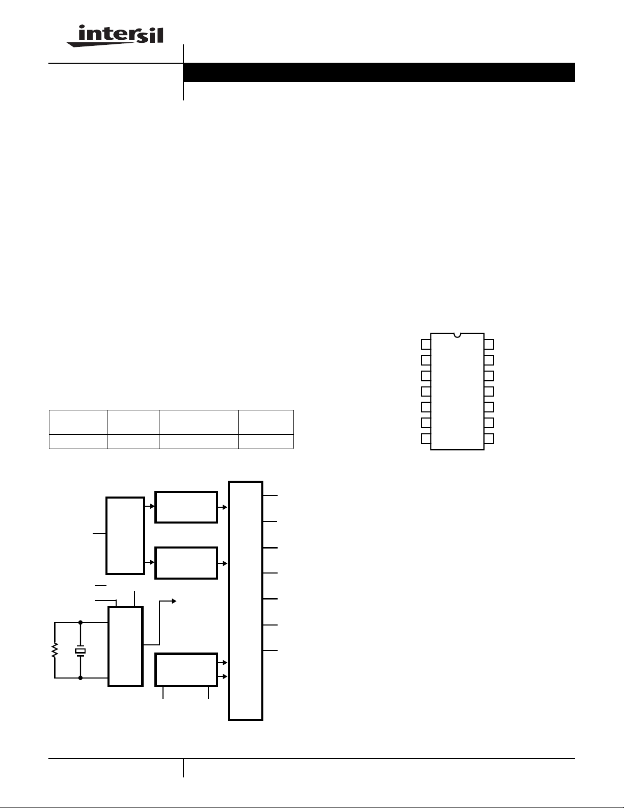
Functional Diagram
ATB
XEN
XIN
XOUT
7
PREPROCESSOR/
BANDSPLIT FILTER
11
6
10
CLOCK
9
GENERATOR
V
DD
ANALOG IN
NOTE: Pin numbers are for PDIP.
LOW B/P
FILTERS
HIGH B/P
FILTERS
CHIP
CLOCKS
DETECTORS AND SIGNAL-
VOLTAGE
REG./REF.
48
V
SS
5
NC
12
DV
2
D1
1
D2
14
D4
13
D8
PROCESSING CIRCUITS
3
EN
67
CAUTION: These devices are sensitive to electrostatic discharge; follow proper IC Handling Procedures.
http://www.intersil.com or 407-727-9207 | Copyright © Intersil Corporation 1999

CD22204
Absolute Maximum Ratings (Note 1) Thermal Information
DC Supply Voltage (VDD) (Referenced to VSS Terminal) . . . . . . .7V
Power Dissipation
TA = 25oC (Derate above TA = 25oC at 6.25mW/oC. . . . . . . .65mW
Input Voltage Range
All Inputs Except Analog In . . . . . . . . . . . . . . (VDD 0.5V) to -0.5V
Analog in Voltage Range. . . . . . . . . . . . . (VDD 0.5V) to (VDD -10V)
DC Current into any Input or Output . . . . . . . . . . . . . . . . . . . . . .±20mA
CAUTION: Stresses above those listed in “Absolute Maximum Ratings” may cause permanent damage to the device. This is a stress only rating and operationofthe
device at these or any other conditions above those indicated in the operational sections of this specification is not implied.
Maximum Junction Temperature . . . . . . . . . . . . . . . . . . . . . . .175oC
Maximum Storage Temperature Range. . . . . . . . . . -65oC to 150oC
Maximum Lead Temperature (Soldering 10s) . . . . . . . . . . . . .300oC
Operating Conditions
Temperature Range. . . . . . . . . . . . . . . . . . . . . . . . . . . .0oC to 70oC
Electrical Specifications 0
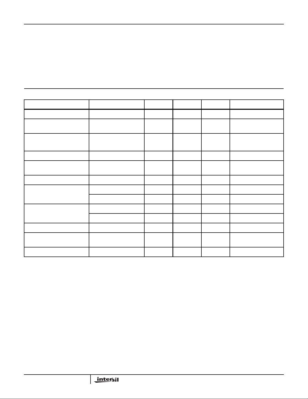
PARAMETER TEST CONDITIONS MIN TYP MAX UNITS
Frequency Detect Bandwidth ±(1.5 + 2Hz) ±2.3 ±3.5 % of f
Amplitude for Detection Each Tone -32
Minimum Acceptable Twist -8 - +4 dB
60Hz Tolerance - - 0.8 V
Dial Tone Tolerance “Precise” Dial Tone - - 0 dB Referenced to Lower
Talk Off MITEL Tape #CM7291 - 2 - Hits
Digital Outputs (except XOUT) “0” Level, 400µA Load 0 - 0.5 V
Digital Inputs “0” Level 0 - 0.3V
Supply Current TA = 25oC - 10 20 mA
Noise Tolerance MITEL Tape #CM7291
o
C ≤ TA≤ 70oC, VDD = 5V ±10%
- -2 dBm Referenced to 600Ω
(Note 3)
Twist
“1” Level, 200µA Load VDD -0.5 - V
“1” Level 0.7V
(Note 2)
High Tone
--------------------------- -=
Low Tone
DD
- - -12 dB Referenced to Lowest
-VDDV
DD
DD
O
RMS
Amplitude Tone
V
V
Amplitude Tone
Input Impedance VDD≥ VIN≥ (VDD -10) 100kΩ//15pF 300kΩ -
NOTES:
1. Unused inputs must be connected to VDD or VSS as appropriate.
2. Bandwidth limited (3kHz) Gaussian noise.
3. Lower minimum available, please contact sales office.
(-32dBm = 19.45mV
, -2dBm = 0.615mV
RMS
RMS
)
68
 Loading...