Intersil Corporation CD14538BMS Datasheet

November 1994
CX1 RX1
CD14538BMS
CMOS Dual Precision
Monostable Multivibrator
Features
• High-Voltage Type (20V Rating)
• Retriggerable/Resettable Capability
• Trigger and Reset Propagation Delays Independent of RX, CX
• Triggering From Leading or Trailing Edge
• Q and
Q Buffered Outputs Available
• Separate Resets
• Wide Range of Output-Pulse Widths
• Schmitt-Trigger Input Allows Unlimited Rise
and Fall Times On +TR and -TR Inputs
• 100% Tested For Maximum Quiescent Current at 20V
• Maximum Input Current of 1µA at 18V Over
Full Package-Temperature Range:
- 100nA at 18V and +25
o
C
• Noise Margin (Full Package-Temperature
Range):
- 1V at VDD = 5V
- 2V at VDD = 10V
- 2.5V at VDD = 15V
• 5V, 10V and 15V Parametric Ratings
• Standardized Symmetrical Output Characteristics
• Meets All Requirements of JEDEC Tentative
Standards No. 13B, “Standard Specifications for Description of “B” Series CMOS
Device’s
Applications
• Pulse Delay and Timing
• Pulse Shaping
Description
CD14538BMS dual precision monostable multivibrator provides stable retriggerable/resettable one-shot operation for any fixed-voltage timing application.
An external resistor (R
accuracy for the circuit. Adjustment of R
put pulse widths from the Q and
output transition (trigger propagation delay) and the time delay from reset input
to output transition (reset propagation delay) are independent of R
cision control of output pulse widths is achieved through linear CMOS techniques.
Leading-edge-triggering (+TR) and trailing-edge-triggering (-TR) inputs are provided for triggering from either edge of an input pulse. An unused +TR input
should be tied to VSS. An unused -TR input should be tied to VDD. A RESET
(on low level) is provided for immediate termination of the output pulse or to prevent output pulses when power is turned on. An unused RESET input should be
tied to VDD. However, if an entire section of the CD14538BMS is not used, its
inputs must be tied to either VDD or VSS. See T able 1.
In normal operation the circuit retriggers (extends the output pulse one period)
on the application of each new trigger pulse. For operation in the non-retriggerable mode,
Q is connected to -TR when leading-edge triggering (+TR) is used
or Q is connected to +TR when trailing-edge triggering (-TR) is used. The time
period (T) for this multivibrator can be calculated by: T = R
The minimum value of external resistance, R
mum values of external capacitance, C
The CD14538BMS is interchangeable with type MC14538 and is similar to and
pin-compatible with the CD4098B* and CD4538B**.
* T = 0.5 RXCX for CX≥ 1000pF.
* T = RXCX; CX min = 5000pF.
The CD14538BMS is supplied in these 16-lead outline packages:
Braze Seal DIP H4X
Frit Seal DIP H1L
Ceramic Flatpack H6W
) and an external capacitor (CX) control the timing and
X
and CX provides a wide range of out-
X
Q terminals. The time delay from trigger input to
and CX. Pre-
X
.
XCX
is 4KΩ. The minimum and maxi-
X
, are 0pF and 100µF, respectively.
X
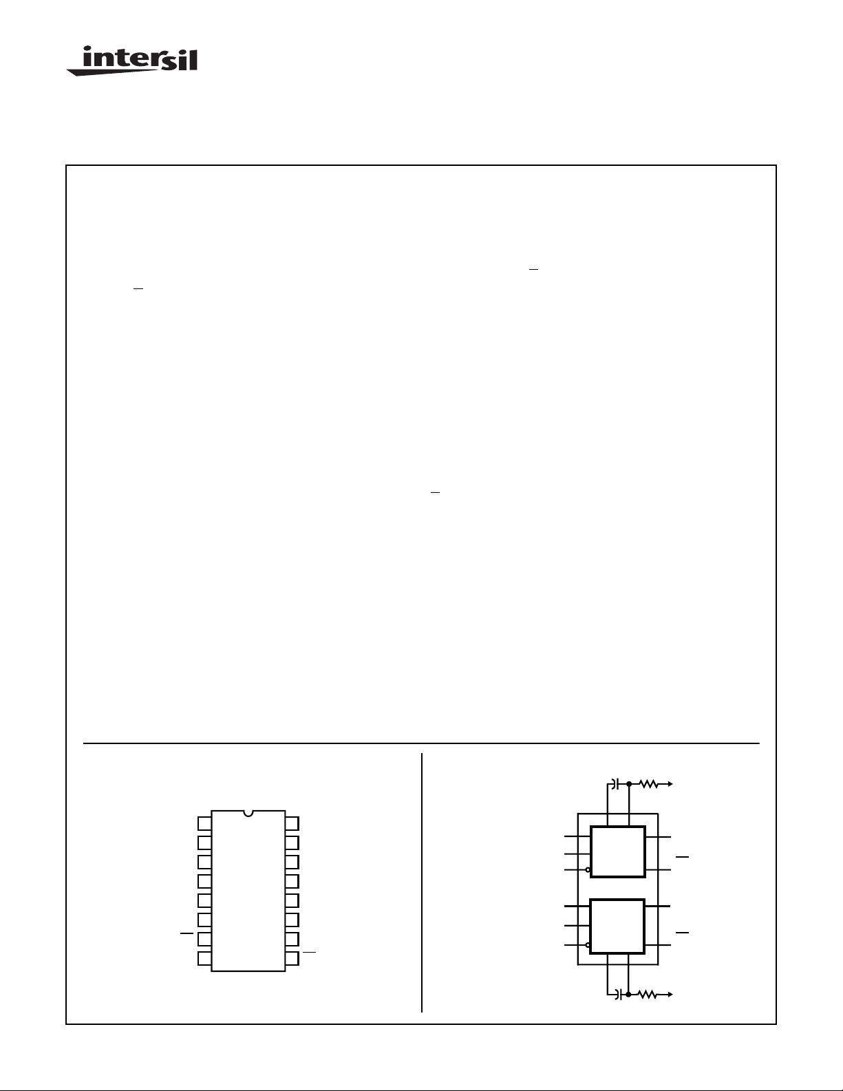
Pinout
CD14538BMS
TOP VIEW
V
1
C
X1
-TR (1)
Q1
Q1
V
SS
2
3
4
5
6
7
8
| Copyright © Intersil Corporation 1999
RXCX (1)
RESET (1)
+TR (1)
CAUTION: These devices are sensitive to electrostatic discharge; follow proper IC Handling Procedures.
http://www.intersil.com or 407-727-9207
16
15
C
14
RXCX (2)
13
RESET (2)
12
+TR (2)
-TR (2)
11
10
Q2
9
Q2
DD
X2
Functional Diagram
7-640
+TR
-TR
RESET
+TR
-TR
RESET
VDD = 16
VSS = 8
4
5
3
12
11
13
15 14 RXCX(2)
21 RXCX(1)
MONO
MONO
CX2 RX2
VDD
Q1
6
1
2
Q1
7
Q2
10
Q2
9
VDD
File Number 3192

Specifications CD14538BMS
Absolute Maximum Ratings Reliability Information
DC Supply Voltage Range, (VDD) . . . . . . . . . . . . . . . -0.5V to +20V
(Voltage Referenced to VSS Terminals)
Input Voltage Range, All Inputs . . . . . . . . . . . . .-0.5V to VDD +0.5V
DC Input Current, Any One Input . . . . . . . . . . . . . . . . . . . . . . . .±10mA
Operating Temperature Range. . . . . . . . . . . . . . . . -55oC to +125oC
Package Types D, F, K, H
Storage Temperature Range (TSTG). . . . . . . . . . . -65oC to +150oC
Lead Temperature (During Soldering) . . . . . . . . . . . . . . . . . +265oC
At Distance 1/16 ± 1/32 Inch (1.59mm ± 0.79mm) from case for
10s Maximum
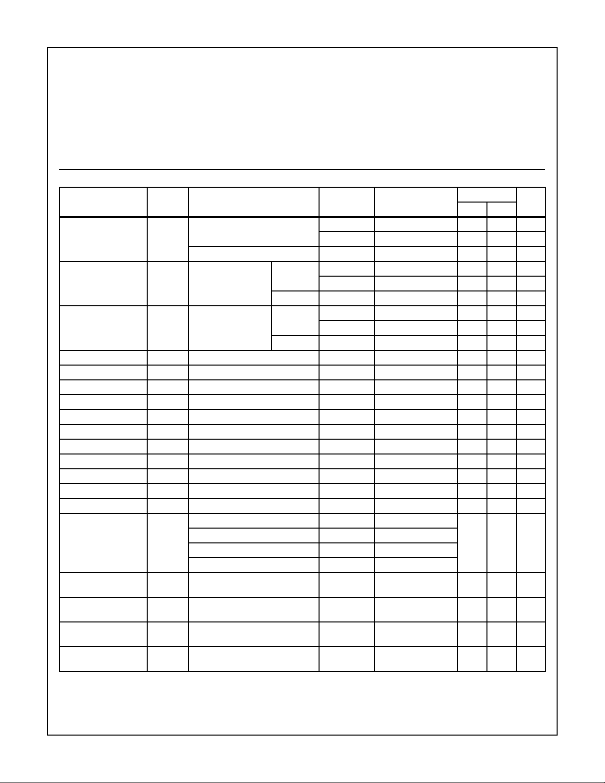
TABLE 1. DC ELECTRICAL PERFORMANCE CHARACTERISTICS
PARAMETER SYMBOL CONDITIONS (NOTE 1)
Supply Current IDD VDD = 20V, VIN = VDD or GND 1 +25oC-10µA
VDD = 18V, VIN = VDD or GND 3 -55oC-10µA
Input Leakage Current IIL VIN = VDD or GND VDD = 20 1 +25oC -100 - nA
VDD = 18V 3 -55oC -100 - nA
Input Leakage Current IIH VIN = VDD or GND VDD = 20 1 +25oC - 100 nA
VDD = 18V 3 -55oC - 100 nA
Output Voltage VOL15 VDD = 15V, No Load 1, 2, 3 +25oC, +125oC, -55oC - 50 mV
Output Voltage VOH15 VDD = 15V, No Load (Note 3) 1, 2, 3 +25oC, +125oC, -55oC 14.95 - V
Output Current (Sink) IOL5 VDD = 5V, VOUT = 0.4V 1 +25oC 0.53 - mA
Output Current (Sink) IOL10 VDD = 10V, VOUT = 0.5V 1 +25oC 1.4 - mA
Output Current (Sink) IOL15 VDD = 15V, VOUT = 1.5V 1 +25oC 3.5 - mA
Output Current (Source) IOH5A VDD = 5V, VOUT = 4.6V 1 +25oC - -0.53 mA
Output Current (Source) IOH5B VDD = 5V, VOUT = 2.5V 1 +25oC - -1.8 mA
Output Current (Source) IOH10 VDD = 10V, VOUT = 9.5V 1 +25oC - -1.4 mA
Output Current (Source) IOH15 VDD = 15V, VOUT = 13.5V 1 +25oC - -3.5 mA
N Threshold Voltage VNTH VDD = 10V, ISS = -10µA 1 +25oC -2.8 -0.7 V
P Threshold Voltage VPTH VSS = 0V, IDD = 10µA 1 +25oC 0.7 2.8 V
Functional F VDD = 2.8V, VIN = VDD or GND 7 +25oC VOH >
VDD = 20V, VIN = VDD or GND 7 +25oC
VDD = 18V, VIN = VDD or GND 8A +125oC
VDD = 3V, VIN = VDD or GND 8B -55oC
Input Voltage Low
(Note 2)
Input Voltage High
(Note 2)
Input Voltage Low
(Note 2)
Input Voltage High
(Note 2)
NOTES: 1. All voltages referenced to device GND, 100% testing being
implemented.
2. Go/No Go test with limits applied to inputs
VIL VDD = 5V, VOH > 4.5V, VOL < 0.5V 1, 2, 3 +25oC, +125oC, -55oC - 1.5 V
VIH VDD = 5V, VOH > 4.5V, VOL < 0.5V 1, 2, 3 +25oC, +125oC, -55oC 3.5 - V
VIL VDD = 15V, VOH > 13.5V,
VOL < 1.5V
VIH VDD = 15V, VOH > 13.5V,
VOL < 1.5V
Thermal Resistance . . . . . . . . . . . . . . . . θ
Ceramic DIP and FRIT Package. . . . . 80oC/W 20oC/W
Flatpack Package . . . . . . . . . . . . . . . . 70oC/W 20oC/W
Maximum Package Power Dissipation (PD) at +125oC
For TA = -55oC to +100oC (Package Type D, F, K). . . . . . 500mW
For TA = +100oC to +125oC (Package Type D, F, K) . . . . .Derate
Linearity at 12mW/oC to 200mW
Device Dissipation per Output Transistor . . . . . . . . . . . . . . . 100mW
For TA = Full Package Temperature Range (All Package Types)
Junction Temperature . . . . . . . . . . . . . . . . . . . . . . . . . . . . . . +175oC
GROUP A
SUBGROUPS TEMPERATURE
2 +125oC - 1000 µA
2 +125oC -1000 - nA
2 +125oC - 1000 nA
1, 2, 3 +25oC, +125oC, -55oC- 4 V
1, 2, 3 +25oC, +125oC, -55oC11 - V
3. For accuracy, voltage is measured differentially to VDD. Limit
is 0.050V max.
ja
LIMITS
VDD/2
VOL <
VDD/2
θ
jc
UNITSMIN MAX
V
7-641

Specifications CD14538BMS
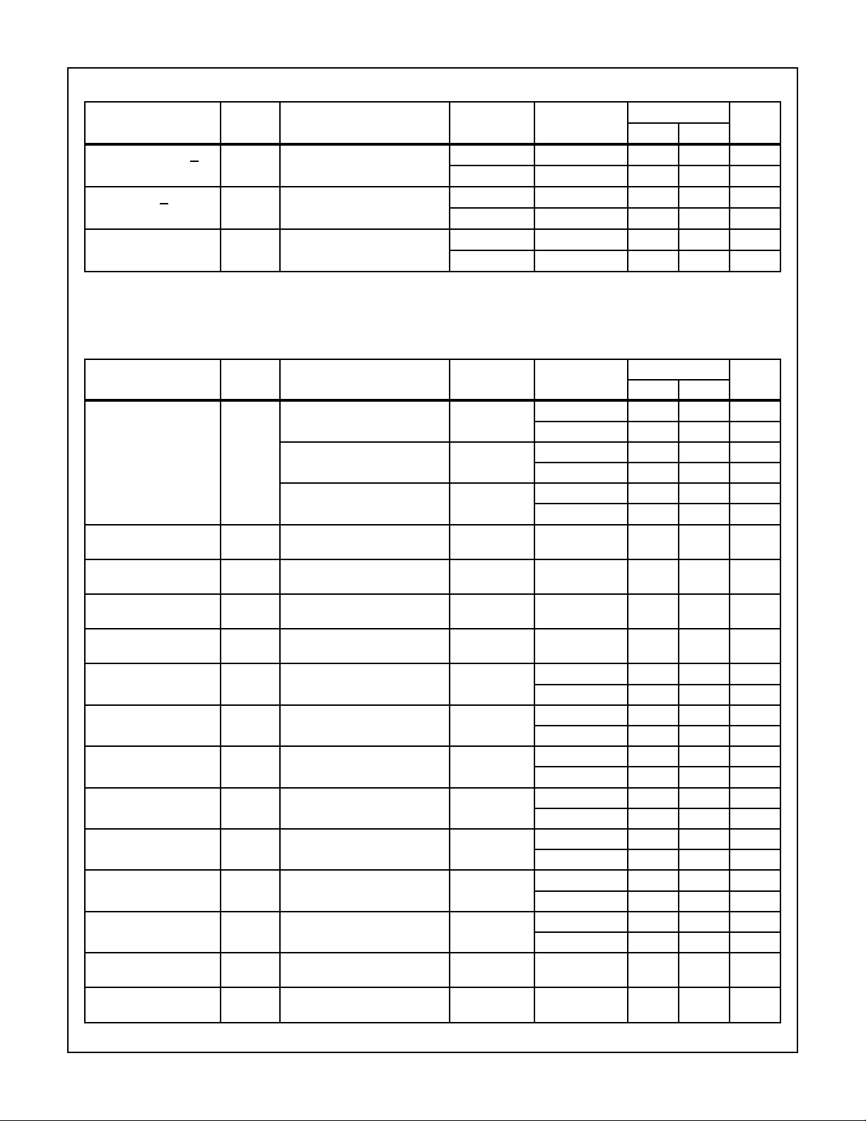
TABLE 2. AC ELECTRICAL PERFORMANCE CHARACTERISTICS
GROUP A
PARAMETER SYMBOL CONDITIONS (Note 1, 2)
Propagation Delay
+TR or -TR to Q or Q
Propagation Delay
Reset to Q or Q
Transition Time TTHL
NOTES:
1. CL = 50pF, RL = 200K, Input TR, TF < 20ns.
2. -55oC and +125oC limits guaranteed, 100% testing being implemented.
PARAMETER SYMBOL CONDITIONS NOTES TEMPERATURE
Supply Current IDD VDD = 5V, VIN = VDD or GND 1, 2 -55oC, +25oC- 5 µA
Output Voltage VOL VDD = 5V, No Load 1, 2 +25oC, +125oC,
Output Voltage VOL VDD = 10V, No Load 1, 2 +25oC, +125oC,
Output Voltage VOH VDD = 5V, No Load 1, 2 +25oC, +125oC,
Output Voltage VOH VDD = 10V, No Load 1, 2 +25oC, +125oC,
Output Current (Sink) IOL5 VDD = 5V, VOUT = 0.4V 1, 2 +125oC 0.36 - mA
Output Current (Sink) IOL10 VDD = 10V, VOUT = 0.5V 1, 2 +125oC 0.9 - mA
Output Current (Sink) IOL15 VDD = 15V, VOUT = 1.5V 1, 2 +125oC 2.4 - mA
Output Current (Source) IOH5A VDD = 5V, VOUT = 4.6V 1, 2 +125oC - -0.36 mA
Output Current (Source) IOH5B VDD = 5V, VOUT = 2.5V 1, 2 +125oC - -1.15 mA
Output Current (Source) IOH10 VDD = 10V, VOUT = 9.5V 1, 2 +125oC - -0.9 mA
Output Current (Source) IOH15 VDD =15V, VOUT = 13.5V 1, 2 +125oC - -2.4 mA
Input Voltage Low VIL1 VDD = 10V , VOH > 9V, VOL < 1V 1, 2 +25oC, +125oC,
Input Voltage High VIH VDD = 10V, VOH > 9V, VOL <
TPHL1
TPLH1
TPHL2
TPLH2
TTLH
VDD = 5V, VIN = VDD or GND 9 +25oC - 600 ns
VDD = 5V, VIN = VDD or GND 9 +25oC - 500 ns
VDD = 5V, VIN = VDD or GND 9 +25oC - 200 ns
TABLE 3. ELECTRICAL PERFORMANCE CHARACTERISTICS
VDD = 10V, VIN = VDD or GND 1, 2 -55oC, +25oC- 10µA
VDD = 15V, VIN = VDD or GND 1, 2 -55oC, +25oC- 10µA
1V
SUBGROUPS TEMPERATURE
10, 11 +125oC, -55oC - 810 ns
10, 11 +125oC, -55oC - 675 ns
10, 11 +125oC, -55oC - 270 ns
+125oC - 150 µA
+125oC - 300 µA
+125oC - 600 µA
-55oC
-55oC
-55oC
-55oC
-55oC 0.64 - mA
-55oC 1.6 - mA
-55oC 4.2 - mA
-55oC - -0.64 mA
-55oC - -2.0 mA
-55oC - -1.6 mA
-55oC - -4.2 mA
-55oC
1, 2 +25oC, +125oC,
-55oC
LIMITS
UNITSMIN MAX
LIMITS
UNITSMIN MAX
-50mV
-50mV
4.95 - V
9.95 - V
-3V
+7 - V
7-642
 Loading...