Intersil Corporation CA555C, CA555 Datasheet

Semiconductor
CA555, CA555C, LM555C
[ /Title
(CA55
5,
CA555
C,
LM555
C)
/Subject
(Timers for
Timing
Delays
and
Oscillator
Applications
in
Commercial,
Industrial
and
Military
Equipment)
/Author
()
/Keywords
(Harris
Semiconductor,
single,
timer,
OBSOLETE PRODUCT
POSSIBLE SUBSTITUTE PRODUCT
ICM7555
Timers for Timing Delays and Oscillator
Applications in Commercial, Industrial
and Military Equipment
The CA555 and CA555C are highly stable timers for use in
precision timing and oscillator applications. As timers, these
monolithic integrated circuits are capable of producing
accurate time delays for periods ranging from microseconds
through hours. These devices are also useful for astable
oscillator operation and can maintain an accurately
controlled free running frequency and duty cycle with only
two external resistors and one capacitor.
The circuits of the CA555 and CA555C may be triggered by
the falling edge of the waveform signal, and the output of
these circuits can source or sink up to a 200mA current or
drive TTL circuits.
These types are direct replacements for industry types in
packages with similar terminal arrangements e.g. SE555
and NE555, MC1555andMC1455,respectively.The CA555
type circuits are intended for applications requiring premium
electrical performance. The CA555C type circuits are
intended for applications requiring less stringent electrical
characteristics.
P AR T NUMBER
(BRAND)
CA0555E -55 to 125 8 Ld PDIP E8.3
CA0555CE 0 to 70 8 Ld PDIP E8.3
LM555CN 0 to 70 8 Ld PDIP E8.3
TEMP.
RANGE (oC) PACKAGE
PKG.
NO.
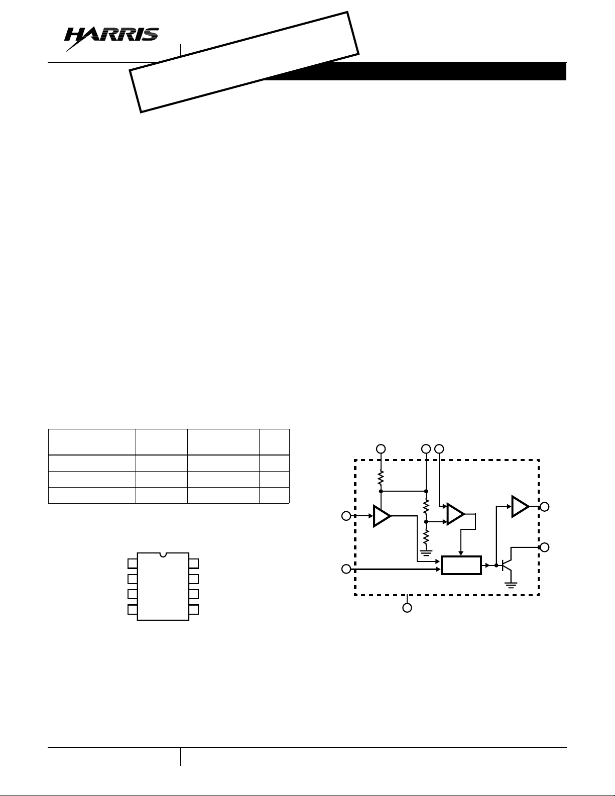
Pinout
CA555, CA555C, LM555C, (PDIP)
TOP VIEW
GND
TRIGGER
OUTPUT
RESET
1
2
3
4
8
V+
7
DISCHARGE
THRESHOLD
6
5
CONTROL
VOLTAGE
December 1999 File Number 834.6
Features
• Accurate Timing From Microseconds Through Hours
• Astable and Monostable Operation
• Adjustable Duty Cycle
• Output Capable of Sourcing or Sinking up to 200mA
• Output Capable of Driving TTL Devices
• Normally ON and OFF Outputs
• High Temperature Stability. . . . . . . . . . . . . . . . 0.005%/
• Directly Interchangeable with SE555, NE555, MC1555,
and MC1455
Applications
• Precision Timing
• Sequential Timing
• Time Delay Generation
• Pulse Generation
• Pulse Detector
• Pulse Width and Position Modulation
Functional Block DiagramPart Number Information
6
THRESHOLD
THRESHOLD
COMP AR
4
RESET
V+
CONTROL
8
VOLTAGE
1
GND
TRIGGER
5
2
FLIP-FLOP
TRIGGER
COMP AR
3
OUTPUT
7
o
C
OUTPUT
DISCHARGE
1
CAUTION: These devices are sensitive to electrostatic discharge; follow proper IC Handling Procedures.
© Harris Corporation 1999
Copyright

CA555, CA555C, LM555C
Absolute Maximum Ratings Thermal Information
DC Supply Voltage. . . . . . . . . . . . . . . . . . . . . . . . . . . . . . . . . . . 18V
Operating Conditions
Temperature Range
CA555 . . . . . . . . . . . . . . . . . . . . . . . . . . . . . . . . . -55oC to 125oC
CA555C, LM555C . . . . . . . . . . . . . . . . . . . . . . . . . . .0oC to 70oC
CAUTION: Stresses above those listed in “Absolute Maximum Ratings” may cause permanent damage to the device. This is a stress only rating and operationofthe
device at these or any other conditions above those indicated in the operational sections of this specification is not implied.
NOTE:
1. θJA is measured with the component mounted on an evaluation PC board in free air.
Thermal Resistance (Typical, Note 1) θJA (oC/W) θJC (oC/W)
PDIP Package . . . . . . . . . . . . . . . . . . . 100 N/A
Maximum Junction Temperature (Plastic Package) . . . . . . . 150oC
Maximum Storage Temperature Range. . . . . . . . . . -65oC to 150oC
Maximum Lead Temperature (Soldering 10s) . . . . . . . . . . . . 300oC
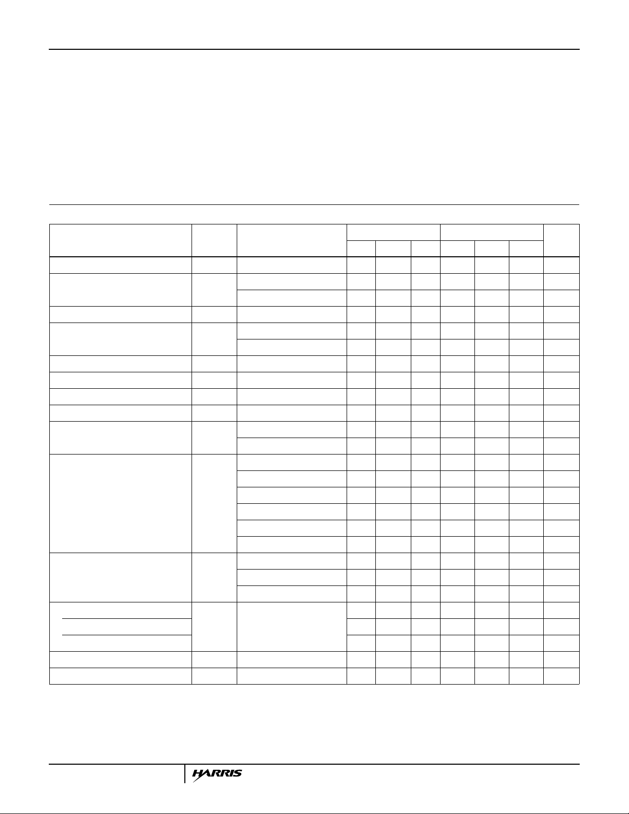
Electrical Specifications T
= 25oC, V+ = 5V to 15V Unless Otherwise Specified
A
CA555 CA555C, LM555C
P ARAMETER SYMBOL TEST CONDITIONS
UNITSMIN TYP MAX MIN TYP MAX
DC Supply Voltage V+ 4.5 - 18 4.5 - 16 V
DC Supply Current (Low State)
(Note 2)
Threshold Voltage V
I+ V+ = 5V, RL = ∞ -35- 36mA
V+ = 15V, RL = ∞ - 10 12 - 10 15 mA
TH
-(2/3)V+ - - (2/3)V+ - V
Trigger Voltage V+ = 5V 1.45 1.67 1.9 - 1.67 - V
V+ = 15V 4.8 5 5.2 - 5 - V
Trigger Current - 0.5 - - 0.5 - µA
Threshold Current (Note 3) I
TH
- 0.1 0.25 - 0.1 0.25 µA
Reset Voltage 0.4 0.7 1.0 0.4 0.7 1.0 V
Reset Current - 0.1 - - 0.1 - mA
Control Voltage Level V+ = 5V 2.9 3.33 3.8 2.6 3.33 4 V
V+ = 15V 9.6 10 10.4 9 10 11 V
Output Voltage V
Low State I
Output Voltage V
High State
Timing Error (Monostable) R1,R2=1kΩ to 100kΩ,
Frequency Drift with Temperature - 30 100 - 50 - ppm/oC
V+ = 5V, I
OL
= 8mA - 0.1 0.25 - - - V
SINK
V+ = 15V, I
I
= 50mA - 0.4 0.5 - 0.4 0.75 V
SINK
I
= 100mA - 2.0 2.2 - 2.0 2.5 V
SINK
I
= 200mA - 2.5 - - 2.5 - V
SINK
V+ = 5V, I
OH
V+ = 15V, I
I
SOURCE
C = 0.1µF
Tested at V+ = 5V, V+ = 15V
= 5mA - - - - 0.25 0.35 V
SINK
= 10mA - 0.1 0.15 - 0.1 0.25 V
SINK
SOURCE
= 100mA 3.0 3.3 - 2.75 3.3 - V
SOURCE
= 100mA
13.0 13.3 - 12.75 13.3 - V
= 200mA - 12.5 - - 12.5 - V
- 0.5 2 - 1 - %
Drift with Supply Voltage - 0.05 0.2 - 0.1 - %/V
Output Rise Time t
Output Fall Time t
R
F
- 100 - - 100 - ns
- 100 - - 100 - ns
NOTES:
2. When the output is in a high state, the DC supply current is typically 1mA less than the low state value.
3. The threshold current will determine the sum of the values of R1 and R2 to be used in Figure 4 (astable operation); the maximum total
R1 + R2 = 20MΩ.
2
 Loading...