November 1996
CA5470
Quad, 14MHz, Microprocessor BiMOS-E
Operational Amplifier with MOSFET Input/Bipolar Output
Features
• High Speed CMOS Input Stage Provides
- Very High Z
- Very Low l
- Very Low I
. . . . . . . . . . . . . . . .5TΩ (5 x 10¹²Ω) (Typ)
I
. . . . . . . . . . . 0.5pA (Typ) at 5V Operation
I
. . . . . . . . . 0.5pA (Typ) at 5V Operation
IO
• ESD Protection to 2000V
• 3V to 16V Power Supply Operation
• Fully Guaranteed Specifications Over Full Military
Range
• Wide BW (14MHz); High SR (5V/µs) at 5V Supply
• Wide V
Range From -0.5V to 3.7V (Typ) at 5V Supply
lCR
• Ideally Suited for CMOS and HCMOS Applications
Applications
• Bar Code Readers
• Photodiode Amplifiers (IR)
• Microprocessor Buffering
• Ground Reference Single Supply Amplifiers
• Fast Sample and Hold
• Timers
• Voltage Controlled Oscillators
• Voltage Followers
• V to l Converters
• Peak Detectors
• Precision Rectifiers
• 5V Logic Systems
• 3V Logic Systems
Description
The CA5470 is an operational amplifier that combines the
advantages of both high speed CMOS and bipolar transistors
on a single monolithic chip. It is constructed in the BiMOS-E
process which adds drain-extension implants to 3µm polygate
CMOS, enhancing both the voltage capability and providing
vertical bipolar transistors for broadband analog/digital functions. This process lends itself easily to high speed operational
amplifiers, comparators, analog switches and interface peripherals, resulting in twice the speed of the conventional CMOS
transistors having similar feature size.
BiMOS-E are broadbased bipolar transistors that have high
transconductance, gains more constant with current level, stable “precision” base-emitter offset voltages and superior drive
capability. Excellent interface with environmental potentials
enable use in 5V logic systems and future 3.3V logic systems.
Refer to Application Note AN8811.
ESD capability exceeds the standard 2000V level. The
CA5470 series can operate with single supply voltages from
3V to 16V or ±1.5V to ±8V. They have guaranteed specifications at both 5V and ±7.5V at room temperature as well as
over the full -55
o
C to 125oC military range.
Ordering Information
PART NUMBER
(BRAND)
CA5470E -55 to 125 14 Ld PDIP E14.3
CA5470M
(5470)
CA5470M96
(5470)
TEMP.
RANGE (oC) PACKAGE
-55 to 125 14 Ld SOIC M14.15
-55 to 125 14 Ld SOIC Tape
and Reel
PKG.
M14.15
NO.
Pinout
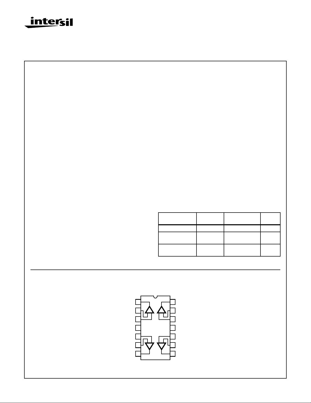
CA5470 (PDIP, SOIC)
TOP VIEW
OUTPUT 1
NEG. INPUT 1
POS. INPUT 1
POS. INPUT 2
NEG. INPUT 2
OUTPUT 2
CAUTION: These devices are sensitive to electrostatic discharge; follow proper IC Handling Procedures.
1-888-INTERSIL or 321-724-7143 | Copyright © Intersil Corporation 1999
V+
1
2
-
3
4
5
-
6
7
14
++
-
++
23
-
3-156
14
OUTPUT 4
13
NEG. INPUT 4
12
POS. INPUT 4
11
V-
10
POS. INPUT 3
9
NEG. INPUT 3
8
OUTPUT 3
File Number
1946.3

CA5470
Absolute Maximum Ratings Thermal Information
DC Supply Voltage (Between V+ And V- Terminals) . . . . . . . . . 16V
Differential Input Voltage. . . . . . . . . . . . . . . . . . . . . . . . . . . . . . . . 8V
Input Voltage. . . . . . . . . . . . . . . . . . . . . . . . . . (V+ +8V) to (V- -0.5V)
Input Current. . . . . . . . . . . . . . . . . . . . . . . . . . . . . . . . . . . . . . . .1mA
Output Short Circuit Duration (Note 1) . . . . . . . . . . . . . . . . Indefinite
Operating Conditions
Temperature Range . . . . . . . . . . . . . . . . . . . . . . . . .-55oC to 125oC
CAUTION: Stresses above those listed in “Absolute Maximum Ratings” may cause permanent damage to the device. This is a stress only rating and operation
of the device at these or any other conditions above those indicated in the operational sections of this specification is not implied.
NOTES:
1. Short circuit may be applied to ground or to either supply.
2. θJA is measured with the component mounted on an evaluation PC board in free air.
Thermal Resistance (Typical, Note 1) θJA (oC/W)
PDIP Package. . . . . . . . . . . . . . . . . . . . . . . . . . . . . 80
SOIC Package. . . . . . . . . . . . . . . . . . . . . . . . . . . . . 175
Maximum Junction Temperature (Die). . . . . . . . . . . . . . . . . . . . 175oC
Maximum Junction Temperature (Plastic Package) . . . . . . . . 150oC
Maximum Storage Temperature Range . . . . . . . . . -65oC to 150oC
Maximum Lead Temperature (Soldering 10s) . . . . . . . . . . . . . 300oC
(SOIC - Lead Tips Only)
Electrical Specifications Typical Values Intended Only for Design Guidance at V+ = 5V, V- = 0V, T
= 25oC, Unless Otherwise Specified
A
PARAMETER SYMBOL TEST CONDITIONS TYPICAL VALUES UNITS
Input Resistance R
Input Capacitance C
Unity Gain Crossover Frequency f
I
I
T
Slew Rate SR V
f = 1MHz 3.1 pF
= 3.65V
OUT
P-P
5TΩ
14 MHz
5V/µs
Transient Response: CL = 25pF, RL= 2kΩ
Rise Time/Fall Time t
r
(Voltage Follower)
27/25 ns
Overshoot OS 20 %
Settling Time (To <0.1%, VIN = 4V
)t
P-P
S
CL = 25pF, RL= 2kΩ
1 µs
(Voltage Follower)
Full Power BW, SR = 5V/µs FPBW AV = 1, V
Electrical Specifications T
= 25oC, V+ = 5V, V- = GND
A
OUT
= 3.65V
P-P
436 kHz
PARAMETER SYMBOL TEST CONDITIONS MIN TYP MAX UNITS
Input Offset Voltage |VIO|-622mV
Input Offset Current |IIO| - 0.5 50 (Note 3) pA
Input Current I
Common Mode Input Range V
I
ICR
Common Mode Rejection Ratio CMRR V
= 0V to 3.5V 55 70 - dB
ICR
- 0.5 50 (Note 3) pA
3.5 -0.5 to 3.7 0 V
Power Supply Rejection Ratio PSRR ∆V = 2V 60 75 - dB
Positive Output Voltage Swing VOM+R
Negative Output Voltage Swing VOM-R
Total Supply Current I
Unity Gain Bandwidth Product f
SUPPLY
T
= 2kΩ to GND 4 4.4 - V
L
= 2kΩ to GND - 0.06 0.10 V
L
V
= 2.5V, RL = ∞ -67mA
OUT
10 14 - MHz
Slew Rate SR 4 5 - V/µs
Output Current
Source to opposite supply I
SOURCE
Sink to opposite supply I
Open Loop Gain A
SlNK
OL
0.5V to 3.5V, RL = 10kΩ 80 90 - dB
4 5.5 - mA
1.0 1.2 - mA
NOTE:
3. This is the lowest value that can be tested reliably. Almost all devices will be <10pA.
3-157
 Loading...