August 1997
CA3310, CA3310A
CMOS, 10-Bit, A/D Converters
with Internal Track and Hold
Features
• CMOS Low Power (Typ). . . . . . . . . . . . . . . . . . . . .15mW
• Single Supply Voltage . . . . . . . . . . . . . . . . . . . .3V to 6V
• Conversion Time . . . . . . . . . . . . . . . . . . . . . . . . . . . 13µs
• Built-In Track and Hold
• Rail-to-Rail Input Range
• Latched Three-state Output Drivers
• Microprocessor-Compatible Control Lines
• Internal or External Clock
Applications
• Fast, No-Droop, Sample and Hold
• Voice Grade Digital Audio
• DSP Modems
• Remote Low Power Data Acquisition Systems
• µP Controlled Systems
Description
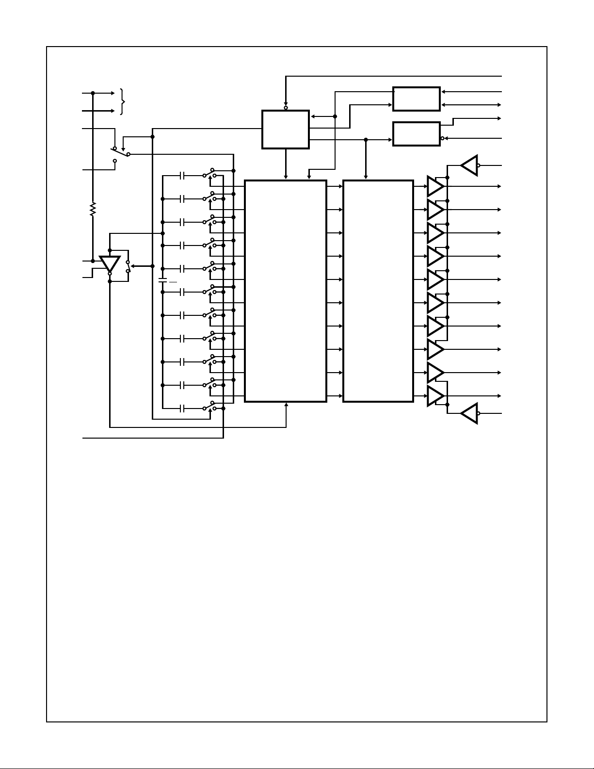
The Intersil CA3310 is a fast, low power, 10-bit successive
approximation analog-to-digital converter, with microprocessorcompatible outputs. It uses only a single 3V to 6V supply and
typically draws just 3mA when operating at 5V. It can accept full
rail-to-rail input signals, and features a built-in track and hold.
The track and hold will follow high bandwidth input signals , as it
has only a 100ns (typical) input time constant.
The ten data outputs feature full high-speed CMOS threestate bus driver capability, and are latched and held through
a full conversion cycle. Separate 8 MSB and 2 LSB enables,
a data ready flag, and conversion start and ready reset
inputs complete the microprocessor interface.
An internal, adjustable clock is provided and is available as
an output. The clock may also be driven from an external
source.
Ordering Information
PART
NUMBER
CA3310E ±0.75 LSB -40 to 85 24 Ld PDIP E24.6
CA3310AE ±0.5 LSB -40 to 85 24 Ld PDIP E24.6
CA3310M ±0.75 LSB -40 to 85 24 Ld SOIC M24.3
LINEARITY
(INL, DNL)
TEMP.
RANGE (oC) PACKAGE
PKG.
NO.
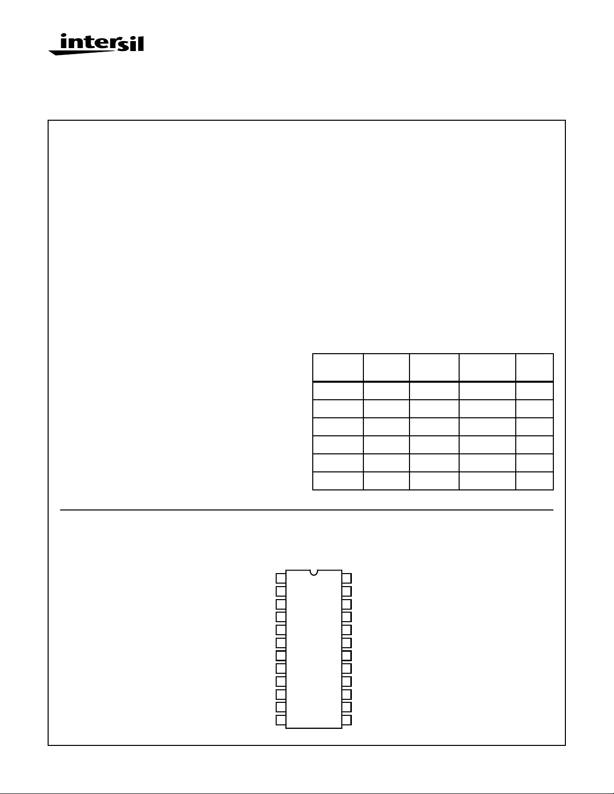
Pinout
D0 (LSB)
D1
D2
D3
D4
D5
D6
D7
D8
D9 (MSB)
DRDY
VSS (GND)
CA3310AM ±0.5 LSB -40 to 85 24 Ld SOIC M24.3
CA3310D ±0.75 LSB -55 to 125 24 Ld SBDIP D24.6
CA3310AD ±0.5 LSB -55 to 125 24 Ld SBDIP D24.6
CA3310, CA3310A
(PDIP, SBDIP, SOIC)
TOP VIEW
1
2
3
4
5
6
7
8
9
10
11
12
24
V
DD
V
23
IN
22
V
+
REF
21
R
EXT
20
CLK
19
STRT
18
V
-
REF
17
+
V
AA
16
-
V
AA
15
OEL
OEM
14
13
DRST
CAUTION: These devices are sensitive to electrostatic discharge; follow proper IC Handling Procedures.
1-888-INTERSIL or 321-724-7143 | Copyright © Intersil Corporation 1999
6-6
File Number 3095.1
Functional Block Diagram
V
DD
V
SS
V
IN
ALL
LOGIC
CA3310, CA3310A
CONTROL
AND
TIMING
CLOCK
CLK CLR
STRT
R
EXT
CLK
Q
DRDY
DRST
V
V
REF
V
V
REF
AA
AA
+
50Ω
SUBSTRATE
RESISTANCE
+
-
-
16C
8C
4C
2C
C
32
C
31
16C
8C
4C
2C
C
C
10-BIT
SUCCESSIVE
APPROXIMATION
REGISTER
10-BIT
EDGE
TRIGGERED
“D”
LATCH
OEM
D9 (MSB)
D8
D7
D6
D5
D4
D3
D2
D1
D0 (LSB)
OEL
6-7
Typical Application Schematics
CA3310, CA3310A
4
A
V
IN
8
ICL7663S
R2
A
R1
+
R4
-1V
TO
-15V
+
4.7µF
TAN
100Ω ±10% 4.5V
3
8
10K
75V
5K
28.7K
100
0.1
6
5
ADJUST
OFF SET
1
6
ADJUST
GAIN
5
R3
7
3
+
2
CA3140
-
1
4
0.1
A
100
4.7µF
TAN
A
+8V
TO
+15V
A
A
+
A
OPTIONAL
CLAMP
V
DD
47pFR5
V
VAA+
+
V
REF
-
V
REF
A
A
CA3310/A
V
-
AA
V
IN
AD
DD
STRT
DRST
OEM
OEL
D0 - D9
DRDY
CLK
R
EXT
V
SS
D
+5V SUPPLY
0.1µF CER
D
START CONVERSATION
RESET FLAG
HIGH BYTE ENABLE
LOW BYTE ENABLE
OUTPUT DATA
DATA READY FLAG
2MHz CLOCK
NC
UNLESS NOTED,
ALL RESISTORS =
1% METAL FILM,
POTS = 10 TURN, CERMET
D = DIGITAL GROUND
A = ANALOG GROUND
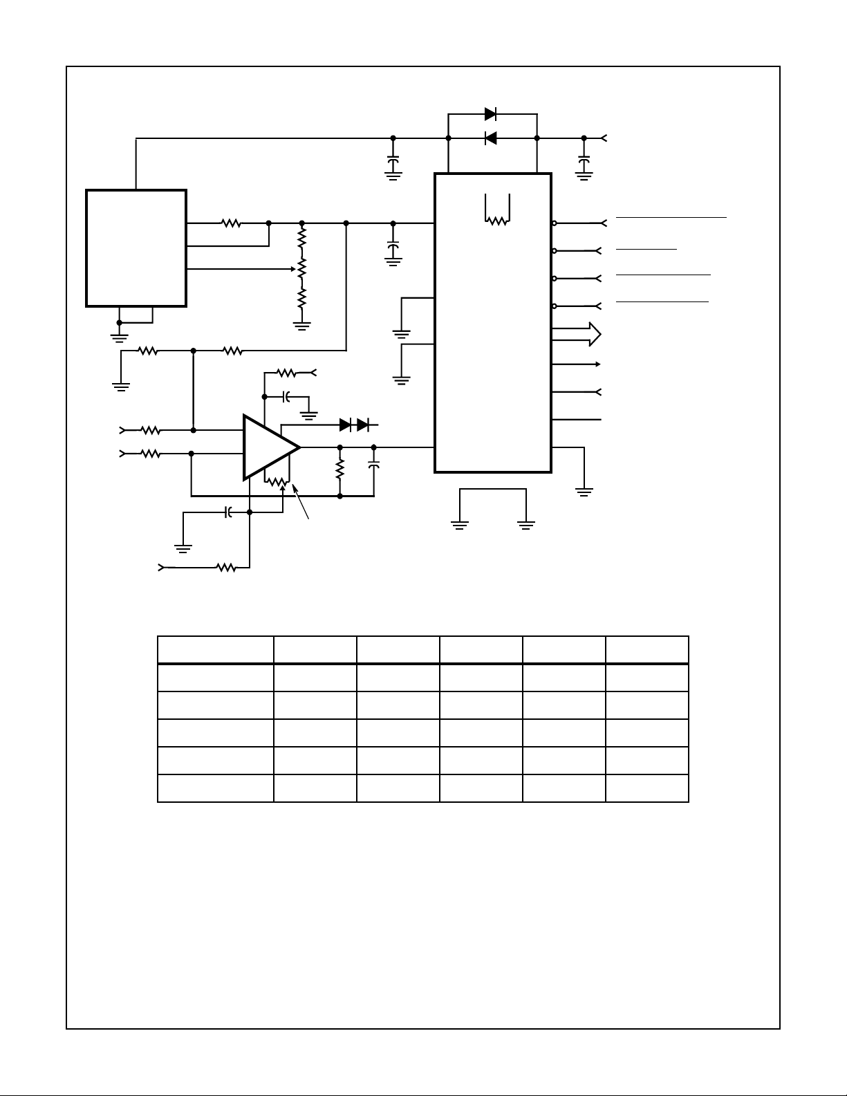
INPUT RANGE R1 R2 R3 R4 R5
0V TO 2.5V 4.99K 9.09K OPEN 4.99K 9.09K
0V TO 5V 4.99K 4.53K OPEN 4.99K 4.53K
0V TO 10V 10K 4.53K OPEN 10K 4.53K
-2.5V TO +2.5V 4.99K 9.09K 9.09K 4.99K 4.53K
-5V TO +5V 10K 9.09K 9.09K 10K 4.53K
6-8
CA3310, CA3310A
Absolute Maximum Ratings Thermal Information
Digital Supply Voltage VDD. . . . . . . . . . . . . . .VSS -0.5V to VSS +7V
Analog Supply Voltage (VAA+) . . . . . . . . . . . . . . . . . . . . .VDD±0.5V
Any Other Terminal. . . . . . . . . . . . . . . . .VSS -0.5V to VDD + 0.5V
DC Input Current or Output (Protection Diode)
Current . . . . . . . . . . . . . . . . . . . . . . . . . . . . . . . . . . . . . . . ±20mA
DC Output Drain Current, per Output. . . . . . . . . . . . . . . . . . ±35mA
Total DC Supply or Ground Current . . . . . . . . . . . . . . . . . . . ±70mA
Operating Conditions
Temperature Range (TA)
Package Type D . . . . . . . . . . . . . . . . . . . . . . . . . . -55oC to 125oC
Package Type E, M. . . . . . . . . . . . . . . . . . . . . . . . . -40oC to 85oC
CAUTION: Stresses above those listed in “Absolute Maximum Ratings” may cause permanent damage to the device. This is a stress only rating and operation
of the device at these or any other conditions above those indicated in the operational sections of this specification is not implied.
NOTE:
1. θJA is measured with the component mounted on an evaluation PC board in free air.
Thermal Resistance (Typical, Note 1) θJA (oC/W) θJC (oC/W)
PDIP Package. . . . . . . . . . . . . . . . . . . . . 75 N/A
SBDIP Package. . . . . . . . . . . . . . . . . . . . 70 22
SOIC Package. . . . . . . . . . . . . . . . . . . . . 75 N/A
Maximum Junction Temperature
Plastic Packages. . . . . . . . . . . . . . . . . . . . . . . . . . . . . . . . .150oC
Hermetic Package. . . . . . . . . . . . . . . . . . . . . . . . . . . . . . . .175oC
Maximum Storage Temperature (T
) . . . . . . . . . .-65oC to 150oC
STG
Maximum Lead Temperature (Soldering 10s). . . . . . . . . . . . 300oC
(SOIC - Lead Tips Only)
Electrical Specifications T
= 25oC, VDD = VAA+ = 5V, V
A
+ = 4.608V, VSS = VAA- = V
REF
- = GND, CLK = External 1MHz,
REF
Unless Otherwise Specified
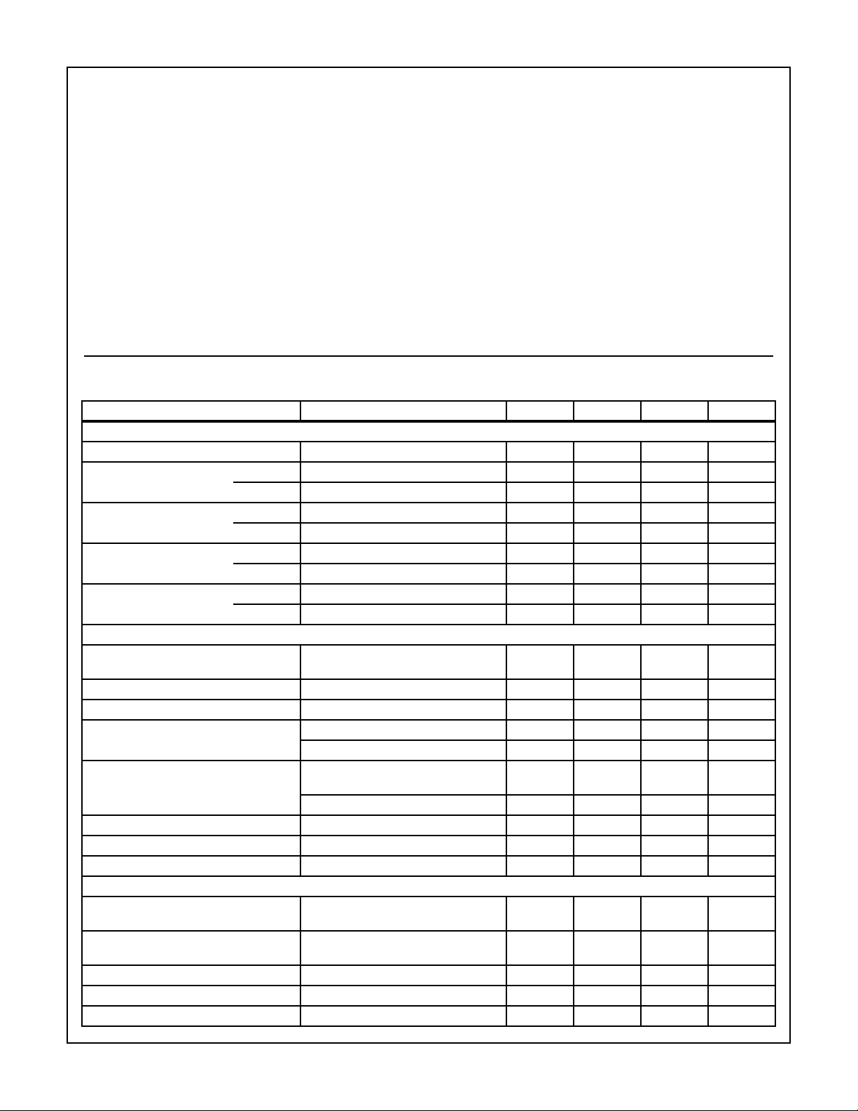
PARAMETER TEST CONDITIONS MIN TYP MAX UNITS
ACCURACY (See Text For Definitions)
Resolution 10 - - Bits
Differential Linearity Error CA3310 - ±0.5 ±0.75 LSB
CA3310A - ±0.25 ±0.5 LSB
Integral Linearity Error CA3310 - ±0.5 ±0.75 LSB
CA3310A - ±0.25 ±0.5 LSB
Gain Error CA3310 - ±0.25 ±0.5 LSB
CA3310A - - ±0.25 LSB
Offset Error CA3310 - ±0.25 ±0.5 LSB
CA3310A - - ±0.25 LSB
ANALOG OUTPUT
Input Resistance In Series with Input Sample
- 330 - Ω
Capacitors
Input Capacitance During Sample State - 300 - pF
Input Capacitance During Hold State - 20 - pF
Input Current At V
Static Input Current STRT = V+, CLK = V+
Input + Full-Scale Range (Note 2) V
Input - Full-Scale Range (Note 2) VSS-0.3 - V
= V
IN
At VIN = V
At VIN = V
At VIN = V
+ = 5V - - +300 µA
REF
- = 0V - - -100 µA
REF
--1µA
+ = 5V
REF
- = 0V - - -1 µA
REF
- +1 - VDD +0.3 V
REF
+ -1 V
REF
Input Bandwidth From Input RC Time Constant - 1.5 - MHz
DIGITAL INPUTS DRST, OEL, OEM, STRT, CLK
High-Level Input Voltage Over VDD = 3V to 6V (Note 2) 70 - - % of
V
Low-Level Input Voltage Over VDD = 3V to 6V (Note 2) - - 30 % of
V
Input Leakage Current Except CLK - - ±1 µA
Input Capacitance (Note 2) - - 10 pF
Input Current CLK Only (Note 2) - - ±400 µA
DD
DD
6-9
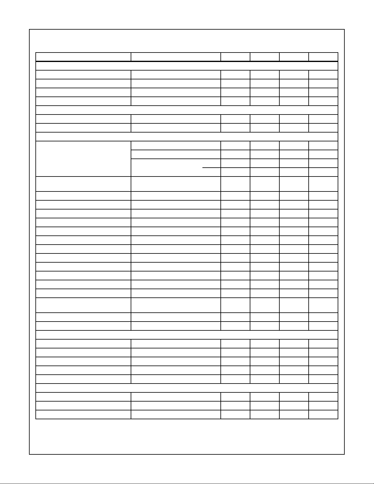
CA3310, CA3310A
Electrical Specifications T
= 25oC, VDD = VAA+ = 5V, V
A
+ = 4.608V, VSS = VAA- = V
REF
- = GND, CLK = External 1MHz,
REF
Unless Otherwise Specified (Continued)
PARAMETER TEST CONDITIONS MIN TYP MAX UNITS
DIGITAL OUTPUTS D0 - D9, DRDY
High-Level Output Voltage I
Low-Level Output Voltage I
SOURCE
SINK
= -4mA 4.6 - - V
= 6mA - - 0.4 V
Three-State Leakage Except DRDY - - ±1 µA
Output Capacitance Except DRDY (Note 2) - - 20 pF
CLK OUTPUT
High-Level Output Voltage I
Low-Level Output Voltage I
SOURCE
SlNK
= 100µA (Note 2) 4 - - V
= 100µA (Note 2) - - 1 V
TIMING
Clock Frequency Internal, CLK and R
Internal, CLK Shorted to R
Open 200 300 400 kHz
EXT
EXT
600 800 1000 kHz
External, Applied to CLK (Note 2) (Max) - 4 2 MHz
(Min) 100 10 - kHz
Clock Pulse Width, t
LOW
, t
HIGH
External, Applied to CLK:
100 - - ns
See Figure 1 (Note 2)
Conversion Time Internal, CLK Shorted to R
EXT
13 - - µs
Aperture Delay, tD APR See Figure 1 - 100 - ns
Clock to Data Ready Delay, tD1 DRDY See Figure 1 - 150 - ns
Clock to Data Ready Delay, tD2 DRDY See Figure 1 - 250 - ns
Clock to Data Delay, tD Data See Figure 1 - 200 - ns
Start Removal Time, tR STRT See Figures 3 and 4 (Note 1) - -120 - ns
Start Setup Time, tSU STRT See Figure 4 - 160 - ns
Start Pulse Width, tW STRT See Figures 3 and 4 - 10 - ns
Start to Data Ready Delay, tD3 DRDY See Figures 3 and 4 - 170 - ns
Clock Delay from Start, tD CLK See Figure 3 - 200 - ns
Ready Reset Removal Time, tR DRST See Figure 50 (Note 1) - -80 - ns
Ready Reset Pulse Width, tW DRST See Figure 5 - 10 - ns
Ready Reset to Data Ready Delay,
See Figure 5 - 35 - ns
tD4 DRDY
Output Enable Delay, t
Output Disable Delay, t
EN
DIS
See Figure 2 - 40 - ns
See Figure 2 - 50 - ns
SUPPLIES
Supply Operating Range, VDD or V
Supply Current, IDD + I
AA
AA
(Note 2) 3 - 6 V
See Figures 14, 15 - 3 8 mA
Supply Standby Current Clock Stopped During Cycle 1 - 3.5 - mA
Analog Supply Rejection At 120Hz, See Figure 13 - 25 - mV/V
Reference Input Current See Figure 10 - 160 - µA
TEMPERATURE DEPENDENCY
Offset Drift At 0 to 1 Code Transition - -4 - µV/oC
Gain Drift At 1022 to 1023 Code Transition - -6 - µV/oC
Internal Clock Speed See Figure 7 - -0.5 - %/oC
NOTES:
1. A (-) removal time means the signal can be removed after the reference signal.
2. Parameter not tested, but guaranteed by design or characterization.
6-10
 Loading...