Intersil Corporation CA3290A, CA3290 Datasheet

CA3290, CA3290A
Data Sheet September 1998 File Number 1049.3
BiMOS Dual Voltage Comparators
with MOSFET Input, Bipolar Output
The CA3290A and CA3290 types consist of a dual voltage
comparator on a single monolithic chip. The common mode
input voltage range includes ground even when operated
from a single supply. The low supply current drain makes
these comparators suitable for battery operation; their
extremely low input currents allow their use in applications
that employ sensors with extremely high source
impedances. Package options are shown in the table below.
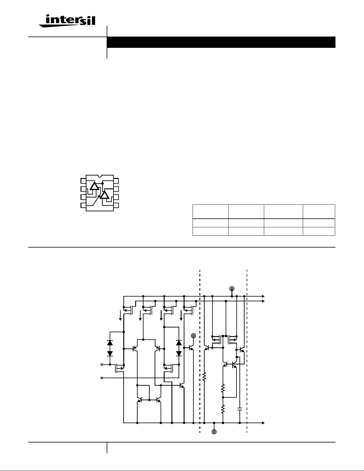
Pinout
CA3290/A (PDIP)
TOP VIEW
OUTPUT (A1)
INV. INPUT (A
NON-INV. INPUT (A
1
A
1
-
)
1
)
1
V-
+
2
3
4
V+
8
OUTPUT (A
7
A
2
-
+
INV. INPUT (A
6
5
NON-INV. INPUT (A
)
2
)
2
)
2
Features
• MOSFET Input Stage
- Very High Input Impedance (Z
) . . . . . . . . 1.7TΩ (Typ)
IN
- Very Low Input Current at V+ = 5V. . . . . . . 3.5pA (Typ)
- Wide Common Mode Input Voltage Range (V
ICR
) Can Be
Swung 1.5V (Typ) Below Negative Supply Voltage Rail
- Virtually Eliminates Errors Due to Flow of Input Currents
• Output Voltage Compatible with TTL, DTL, ECL, MOS,
and CMOS Logic Systems in Most Applications
Applications
• High Source Impedance Voltage Comparators
• Long Time Delay Circuits
• Square Wave Generators
• A/D Converters
• Window Comparators
Ordering Information
PART
NUMBER
CA3290AE -55 to 125 8 Ld PDIP E8.3
CA3290E -55 to 125 8 Ld PDIP E8.3
TEMP
RANGE (oC) PACKAGE PKG. NO.
Schematic Diagram
I
1
Q
50µA 100µA50µA
D
1
D
2
Q
1
+V
I
-V
I
Q
(ONLY ONE IS SHOWN)
COMPARATOR NO. 1
I
2
9
5
Q2Q
I
3
Q
10
3
Q
6
Q
11
100µA
D
3
D
4
Q
4
BIASING CIRCUIT
FOR CURRENT
SOURCES
V+
I
4
Q
12
V
O
Q
8
Q
7
Q
15
R
1
100kΩ
Q13Q
Q
17
R
2
1kΩ
R
3
5kΩ
Q
5pF
14
18
C
1
TO
COMP.
NO. 2
Q
16
V-
1
CAUTION: These devices are sensitive to electrostatic discharge; follow proper IC Handling Procedures.
1-888-INTERSIL or 321-724-7143
| Copyright © Intersil Corporation 1999

CA3290, CA3290A
Absolute Maximum Ratings Thermal Information
Supply Voltage
Single Supply . . . . . . . . . . . . . . . . . . . . . . . . . . . . . . . . . . . . +36V
Dual Supply. . . . . . . . . . . . . . . . . . . . . . . . . . . . . . . . . . . . . . . . . . ±18V
Differential Input Voltage . . . . . . . . . . . . . . . . 36V or [(V+ - V-) +5V]
(whichever is less)
DC Input Voltage . . . . . . . . . . . . . . . . . . . . . . . . . . V+ +5V to V- -5V
Output to V- Short Circuit Duration (Note 1) . . . . . . . . . .Continuous
Input Current . . . . . . . . . . . . . . . . . . . . . . . . . . . . . . . . . . . . . . . 1mA
Operating Conditions
Temperature Range. . . . . . . . . . . . . . . . . . . . . . . . . . . -55 to 125oC
CAUTION: Stresses above those listed in “Absolute Maximum Ratings” may cause permanent damage to the device. This is a stress only rating and operation of the
device at these or any other conditions above those indicated in the operational sections of this specification is not implied.
NOTES:
1. Short circuits from the output to V+ can cause excessive heating and eventual destruction of the device.
2. θJA is measured with the component mounted on an evaluation PC board in free air.
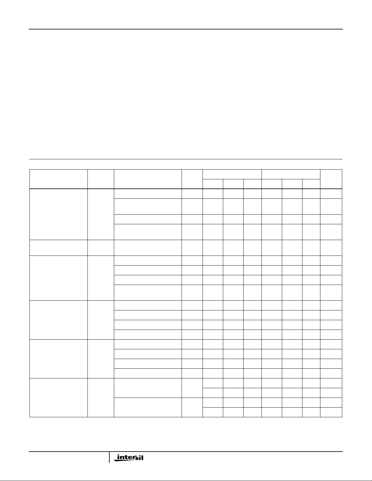
Electrical Specifications V- = 0V, Unless Otherwise Specified
PARAMETER SYMBOL TEST CONDITIONS
Input Offset Voltage V
Temperature Coefficient
of Input Offset Voltage
Input Offset Current I
Input Current I
Supply Current I+ RL = ∞, V+ = 5V -55 - 0.85 1.0 - 0.85 1.6 mA
Voltage Gain A
∆VIO/∆T-8--8-µV/oC
VCM = VO = 1.4V, V+ = 5V Full - 4.5 - - 8.5 - mV
IO
VCM = VO = 0V, V+ = +15V,
V- = -15V
VCM = VO = 1.4V, V+ = 5V 25 - 4.0 10 - 7.5 20 mV
VCM = VO = 0V, V+ = +15V,
V- = -15V
VCM = 1.4V, V+ = 5V Full - 2 28 - 2 32 nA
IO
VCM=0V ,V+ = +15V,V-= -15V Full - 7 28 - 7 32 nA
VCM = 1.4V, V+ = 5V 25 - 2 25 - 2 30 pA
VCM = 0V,
V+ = +15V, V- = -15V
VCM = 1.4V, V+ = 5V 125 - 2.8 45 - 2.8 55 nA
I
VCM=0V ,V+ = +15V,V-= -15V 125 - 13 45 - 13 55 nA
VCM = 1.4V, V+ = 5V 25 - 3.5 40 - 3.5 50 pA
VCM=0V ,V+ = +15V,V-= -15V 25 - 12 40 - 12 50 pA
RL = ∞, V+ = 30V -55 - 1.62 3.0 - 1.62 3.5 mA
RL = ∞, V+ = 5V 25 - 0.8 1.4 - 0.8 1.4 mA
RL = ∞, V+ = 30V 25 - 1.35 3.0 - 1.35 3.0 mA
RL = 15kΩ, V+ = +15V,
OL
V- = -15V
RL = 15kΩ, V+ = +15V ,
V- = -15V
Thermal Resistance (Typical, Note 2) θJA (oC/W) θJC (oC/W)
PDIP Package . . . . . . . . . . . . . . . . . . . 120 N/A
Maximum Junction Temperature (Plastic Package). . . . . . . . .150oC
Maximum Storage Temperature Range. . . . . . . . . . -65oC to 150oC
Maximum Lead Temperature (Soldering 10s) . . . . . . . . . . . . 300oC
TEMP
(oC)
Full - 8.5 - - 8.5 - mV
25 - 4.0 10 - 7.5 20 mV
25 - 7 25 - 7 30 pA
Full - 150 - - 150 - V/mV
25 25 800 - 25 800 - V/mV
CA3290A CA3290
UNITSMIN TYP MAX MIN TYP MAX
- 103 - - 103 - dB
88 118 - 88 118 - dB
2

CA3290, CA3290A
Electrical Specifications V- = 0V, Unless Otherwise Specified (Continued)
TEMP
PARAMETER SYMBOL TEST CONDITIONS
Saturation Voltage V
SATISINK
= 4mA, V+ = 5V,
(oC)
125 - 0.22 0.7 - 0.22 0.7 V
+VI = 0V, -VI = 1V
I
= 4mA, V+ = 5V,
SINK
-55 - 0.1 - - 0.1 - V
+VI = 0V, -VI = 1V
I
= 4mA, V+ = 5V,
SINK
25 - 0.12 0.4 - 0.12 0.4 V
+VI = 0V, -VI = 1V
Output Leakage Current I
V+ = 15V Full - 65 - - 65 - nA
OL
V+ = 36V Full - 130 1k - 130 1k nA
V+ = 15V 25 - 100 - - 100 - pA
V+ = 36V 25 - 500 - - 500 - pA
Common Mode Input
V
VO = 1.4V, V+ = 5V 25 V+-3.5V-V+-3.1
ICR
Voltage Range
VO = 0V, V+ = +15V, V- = -15V 25 V+-3.8V-V+-3.4
Common Mode
Rejection Ratio
Power Supply Rejection
CMRR V+ = +15V, V- = -15V 25 - 44 562 - 44 562 µV/V
V+ = 5V 25 - 100 562 - 100 562 µV/V
PSRR V+ = +15V, V- = -15V 25 - 15 316 - 15 316 µV/V
Ratio
Output Sink Current VO = 1.4V, V+ = 5V 25 6 30 - 6 30 - mA
Response Time Rising
t
RL = 5.1kΩ, V+ = 15V 25 - 1.2 - - 1.2 - µs
r
Edge
Response Time Falling
t
RL = 5.1kΩ, V+ = 15V 25 - 200 - - 200 - ns
f
Edge
Large Signal Response
Time
RL = 5.1kΩ, V+ = 15V 25 - 500 - - 500 - ns
RL = 5.1kΩ, V+ = 5V 25 - 400 - - 400 - ns
CA3290A CA3290
- V+-3.5V-V+-3.1
V- -1.5
V- -1.5
- V+-3.8V-V+-3.4
V- -1.6
V- -1.6
UNITSMIN TYP MAX MIN TYP MAX
-V
-V
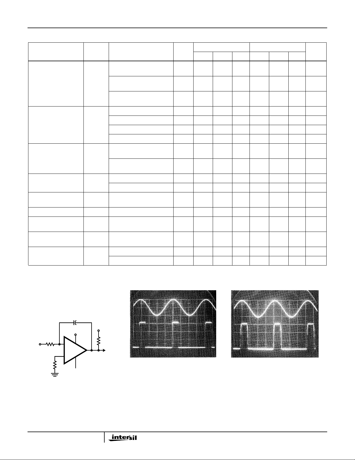
Test Circuits and Waveforms
CC = 2pF
+15V
1K
V
IN
+
-
1K
-15V
+15V
TO 10X
SCOPE
PROBE
FIGURE 1. PARASITIC OSCILLATIONS TEST CIRCUIT AND WAVEFORMS
3
WITH C
C
Top Trace ≈ 4.5mV/Div. = V
Bottom Trace = 10V/Div. = V
Time Scale = 5µs/Div.
OUT
WITHOUT C
IN
Top Trace ≈ 4.5mV/Div.
C
Bottom Trace = 10V/Div.
Time Scale = 5µs/Div.
 Loading...