Intersil Corporation CA3282 Datasheet

June 1998
CA3282
Octal Low Side Power Driver
with Serial Bus Control
Features
• Output Current Drive Capability
- All Outputs ON, Equal . . . . . . . . . . . . . . 0.625A Each
- Per Output Individually . . . . . . . . . . . . . . . . . 1A Each
- Maximum Total of Outputs ON . . . . . . . . . . . . . . . .5A
• High Voltage Power BiMOS Outputs
- 8 Open Drain NDMOS Drivers
- Individual Output Latch
- Over-Current Limit Protection . . . . . . . . . . . . . 1.05A
- Over-Voltage Clamp Protection. . . . . . . . . . . . . . .30V
• High Speed CMOS Logic Control
- Low Quiescent I
Current. . . . . . . . . . . . . . . . . 5mA
DD
- SPI Bus Controlled Interface
- Individual Fault Unlatch and Feedback
- Common Reset Line
• Operating Temperature Range. . . . . . . -40
o
C to 125oC
Applications
• Automotive and Industrial Systems
• Solenoids, Relays and Lamp Drivers
• Logic and µP Controlled Drivers
• Robotic Controls
Description
The CA3282 is a logic controlled, eight channel octal power
driven. The serial peripheral interface (SPI) utilized by the
CA3282 is a serial synchronous bus compatible with Intersil
CDP68HC05, or equivalent, microcomputers. As shown in
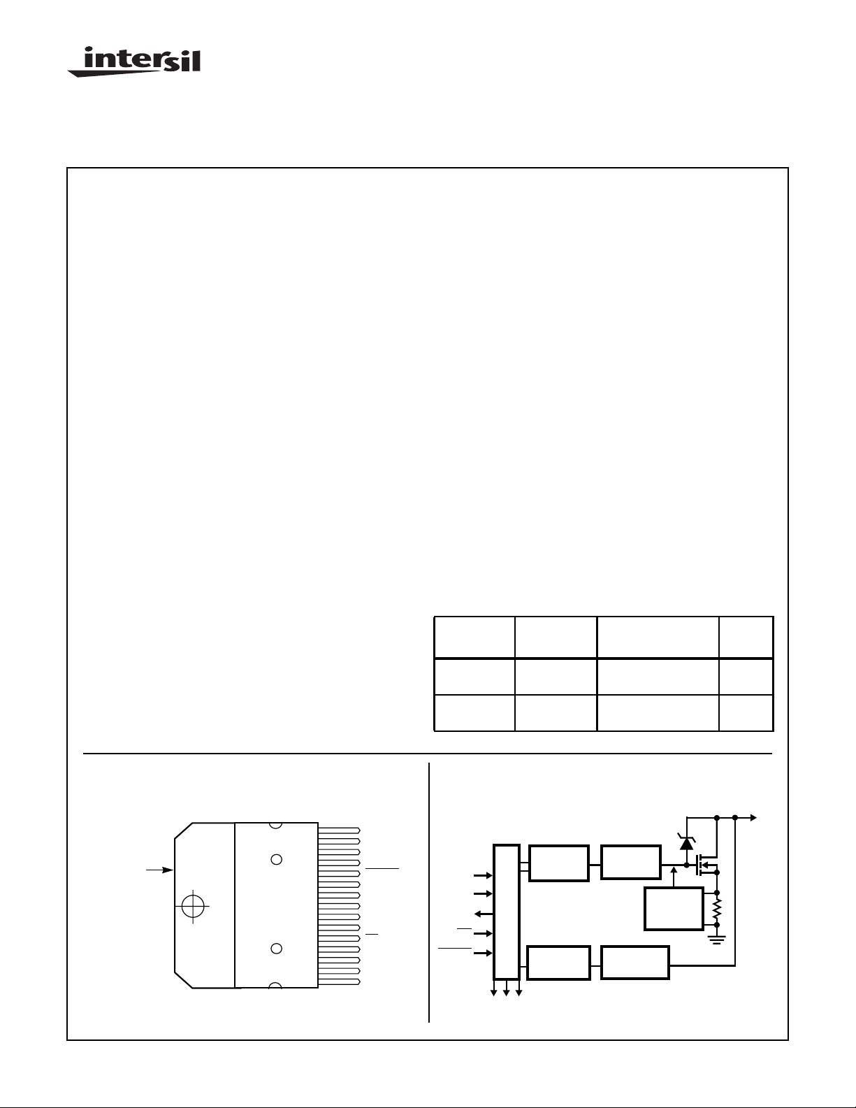
the Block Diagram for the CA3282 each of the open drain
NDMOS output drivers has individual protection for over-voltage and over-current. Each output channel has separate
output latch control with fault unlatch and diagnostic feedback. Under normal ON conditions, each output driver is in a
low, saturation state. Comparators in the diagnostic circuitry
monitor the output drivers to determine if an out of saturation
condition exists. If a comparator senses a fault, the respective output driver is unlatched. In addition, over current protection is provided with current limiting in each output,
independent of the diagnostic feedback loop.
The CA3282 is fabricated in a PowerBiMOS IC process, and is
intended for use in automotive and other applications having a
wide range of temperature and electrical stress conditions. It is
particularly suited for driving lamps, relays, and solenoids in
applications where low operating power, high breakdown voltage, and high output current at high temperatures is required.
The CA3282 is supplied in 15 lead plastic SIP package with
lead forms for either vertical or surface mount.
Ordering Information
PART
NUMBER
TEMP.
RANGE(oC)
PACKAGE AND
LEAD FORM
PKG
NO.
CA3282AS1 -40 to 125 15 Ld Plastic SIP
CA3282AS2 -40 to 125 15 Ld Plastic SIP
Pinout
CA3282 (SIP)
TOP VIEW
15
14
13
NOTE:
HEAT SINK TAB
INTERNALLY
CONNECTED TO
GROUND (V
CAUTION: These devices are sensitive to electrostatic discharge; follow proper IC Handling Procedures.
http://www.intersil.com or 407-727-9207
SS
)
| Copyright © Intersil Corporation 1999
12
11
10
9
8
7
6
5
4
3
2
1
OUTPUT 4
OUTPUT 5
OUTPUT 6
OUTPUT 7
RESET
V
DD
MISO
V
SS
MOSI
SCK
CE
OUTPUT 0
OUTPUT 1
OUTPUT 2
OUTPUT 3
Block Diagram
MOSI
SCK
MISO
CE
RESET
TO DRIVERS
1 THRU 7
1
SHIFT
REGISTER
CONTROL
SPI INTERFACE CIRCUIT
LOGIC
Staggered Vertical
Surface Mount
OUTPUT
LATCH
CURRENT
LIMIT
DIAGNOSTIC
CIRCUITRY
File Number 2767.6
Z15.05A
Z15.05B
OUTPUT #0
(1 OF 8)

CA3282
Absolute Maximum Ratings Thermal Information
Output Voltage, VO (Note 1). . . . . . . . . . . . . . . . . . . . . VOC(Clamp)
Output Load Current, I
Output Load Current, I
(Per Output, Individual) . . . . . . . . . 1A
LOAD
(All 8 Outputs ON, Equal I
LOAD
OUT
) . . . . .
0.625A
Output Load Current, I
(Max. Total of Outputs ON) . . . . 5.0A
LOAD
DC Logic Supply, VDD . . . . . . . . . . . . . . . . . . . . . . . . . . . . . . . . . 7V
Input Voltage, VIN . . . . . . . . . . . . . . . . . . . . . . . . . . . . . .-0.7 to +7V
Operating Conditions
Ambient Temperature Range . . . . . . . . . . . . . . . . . -40oC to 125oC
Junction Temperature Range . . . . . . . . . . . . . . . . . -40oC to 150oC
CAUTION: Stresses above those listed in “Absolute Maximum Ratings” may cause permanent damage to the device. This is a stress only rating and operation
of the device at these or any other conditions above those indicated in the operational sections of this specification is not implied.
NOTES:
1. The MOSFET Output Drain is internally clamped with a Drain-to-Gate zener diode that turns-on the MOSFET; holding the Drain at the
Output Clamp Voltage, VOC.
2. θJA is measured with the component mounted on an evaluation PC board in free air.
Thermal Resistance (Typical, Note 2) θJA(oC/W) θJC(oC/W)
Plastic SIP
No Heat Sink . . . . . . . . . . . . . . . . . . . 45 N/A
Infinite Heat Sink . . . . . . . . . . . . . . . . . N/A 3
Power Dissipation
Up to 125oC w/o Heat Sink . . . . . . . . . . . . . . . . . . . . . . . . 0.56W
Above 125oC w/o Heat Sink . . . . . . .Derate Linearly at 22mW/oC
Up to 125oC w/Infinite Heat Sink. . . . . . . . . . . . . . . . . . . . 8.33W
Above 125oC w/Infinite Heat Sink. . . . Derate Linearly at 333mW/oC
Maximum Storage Temperature Range . . . . . . . . . -55oC to 150oC
Maximum Lead Temperature (Soldering, 10s). . . . . . . . . . . . . . . 265oC
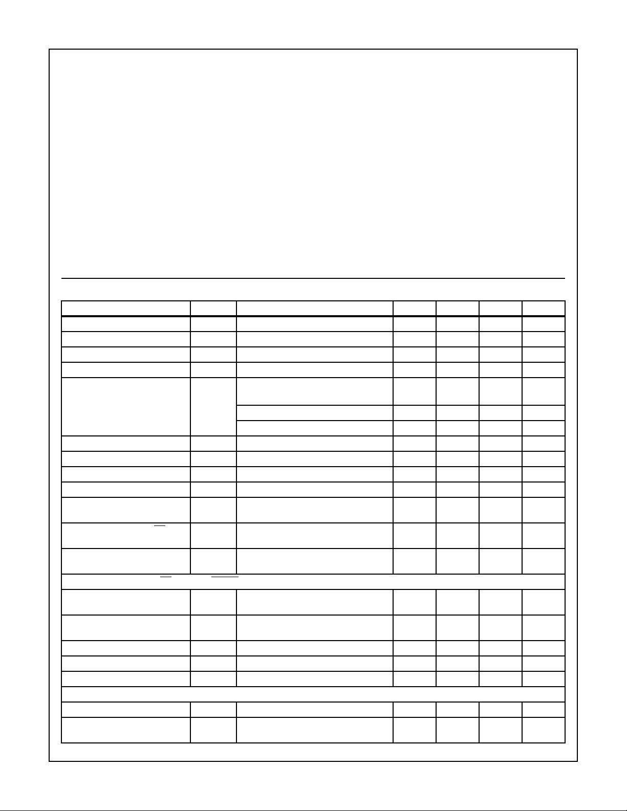
Electrical Specifications V
= 5V, TA = -40oC to 125oC, Unless Otherwise Specified
DD
PARAMETER SYMBOL TEST CONDITIONS MIN TYP MAX UNITS
Quiescent Supply Current, ON I
Quiescent Supply Current, OFF I
Output Clamping Voltage V
Output Clamping Energy E
Output Leakage Current I
Output ON Resistance r
Output Current Limit I
Turn-On Delay t
Turn-Off Delay t
Fault Reference Voltage V
Fault Reset Delay (After CE Low
DD
DD
OC
OC
O LEAK
DS(ON)ILOAD
O LIMIT
PHL
PLH
OREF
t
UD
to High Transition)
Output OFF Voltage V
OFF
LOGIC INPUTS (MOSI, CE, SCK and RESET)
Threshold Voltage at Falling
V
T-
Edge
Threshold Voltage at Rising
V
T+
Edge
Hysteresis Voltage V
Input Current I
Input Capacitance C
H
I
I
LOGIC OUTPUT (MISO)
Output LOW Voltage V
Output HIGH Voltage V
OL
OH
All Outputs ON, 0.5A Load Per Output - 5 10 mA
All Outputs OFF - 0.2 - mA
I
= 0.5A, Output Programmed OFF 27 32 40 V
LOAD
I
= 0.5A, Output ON 20 - - mJ
LOAD
Output Programmed OFF
VO = 24V - 150 1000 µA
VO = 14V - 150 500 µA
VO = 5V - 150 200 µA
= 0.5A (Note 3) - - 1 Ω
Output Programmed ON, V
> 3V 1.05 1.5 - A
OUT
IO = 500mA, No Reactive Load - 1 10 µs
IO = 500mA, No Reactive Load - 2 10 µs
Output Programmed ON, Fault Detected
If VO > V
OREF
1.6 1.8 2.0 V
See Figure 1 50 80 250 µs
Output Programmed OFF, Output Pin
-01V
Floating
VDD = 5V ±10% 0.2V
VDD = 5V ±10% - 0.6V
VT+ - V
T-
VDD = 5.5V, 0 < VI < V
0 < VI < V
DD
DD
0.85 1.4 2.25 V
-10 - +10 µA
- - 20 pF
DD
0.3V
DD
DD
-V
0.7V
DD
V
IOL = 1.6mA - 0.2 0.4 V
IOL = 0.8mA V
- 1.3V
DD
V
DD
- 0.2V
-V
2

CA3282
Electrical Specifications V
= 5V, TA = -40oC to 125oC, Unless Otherwise Specified (Continued)
DD
PARAMETER SYMBOL TEST CONDITIONS MIN TYP MAX UNITS
Output Three State Leakage
Current
Output Capacitance C
I
OL
OUT
VDD = 5.25V, 0 < VO < VDD,
-10 - +10 µA
CE Pin Held High
0 < VO < VDD, CE Pin Held High - - 20 pF
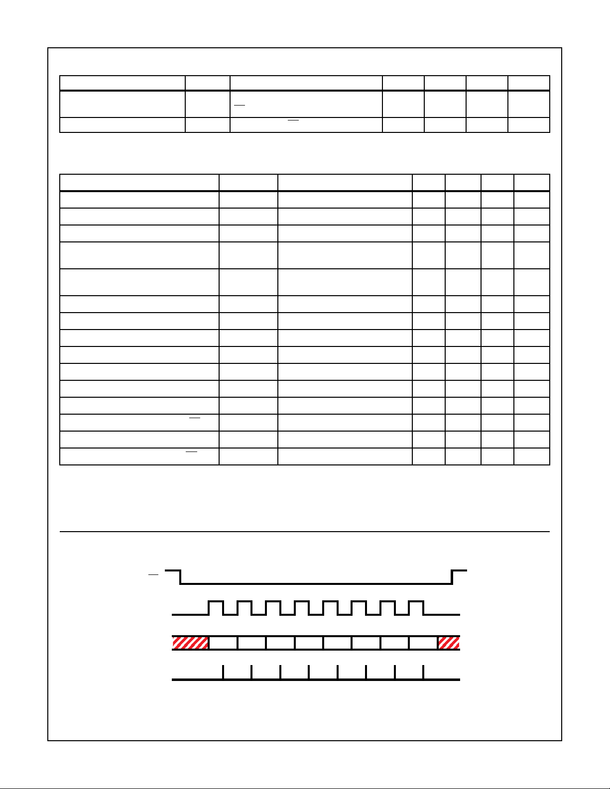
Serial Peripheral Interface Timing (See Figure 1B)
PARAMETER SYMBOL TEST CONDITIONS MIN TYP MAX UNITS
Operating Frequency f
Enable Lead Time (2) t
Enable Lag Time (3) t
Clock HIGH Time (4) t
Clock LOW Time (5) t
Data Setup Time (6) t
Data Hold Time (7) t
Enable Time (8) t
Disable Time (9) t
Data Valid Time (10) t
Output Data Hold Time (11) t
Rise Time (MISO Output) (12) t
Rise Time SPI Inputs (SCK, MOSI, CE) (12) t
Fall Time (MISO Output) (13) t
Fall Time SPI Inputs (SCK, MOSI, CE) (13) t
OPER
LEAD
wSCK
wSCK
LAG
H
L
SU
H
EN
DIS
V
HO
rSOVDD
rSIVDD
fSOVDD
fSIVDD
= 20% to 70%, CL = 200pF - 35 100 ns
= 20% to 70%, CL = 200pF - - 50 ns
= 70% to 20%, CL = 200pF - 45 100 ns
= 70% to 20%, CL = 200pF - - 50 ns
NOTES:
3. Refer to Figure 4A for I
OUT
current vs V
voltage. Typical r
SAT
values are given for -40oC, 25oC, 105oC and 125oC temperatures.
DS(ON)
4. The Maximum Operating Frequency is typically greater than 10MHz but it is application limited primarily by external SPI input rise/fall
times and MISO output loading.
D.C. Note 4 3.0 MHz
- <100 200 ns
- <100 200 ns
- 50 100 ns
- 50 100 ns
-2050ns
-2050ns
- 50 100 ns
- 150 300 ns
- 75 150 ns
050-ns
Timing Diagrams
CE
SCK
(CPOL = 0, CPHA = 1)
MSB 6 5 4 3 2 1 LSB
INTERNAL STROBE FOR DATA CAPTURE
FIGURE 1A. DATA AND CLOCK TIMING DIAGRAM
3
 Loading...