Intersil Corporation CA3275 Datasheet

CA3275
April 1994
Features
• Two Full Bridge Drivers
• ± 150mA Maximum Current
• Logic Controlled Switching
• Direction Control
• PWM I
OUT
Control
• 18V Over-Voltage Protection
• 300mA Short-Circuit Protection
• Nominal 8V to 16V Operation
• Internal Voltage Regulation With Bandgap Reference
Applications
• Dual Full Bridge Driver For Air Core Gauge Instrumentation
• µP Controlled Sensor Data Displays
• Speedometer Displays
• Tachometer Displays
• Stepper Motors
Dual Full Bridge Driver
Description
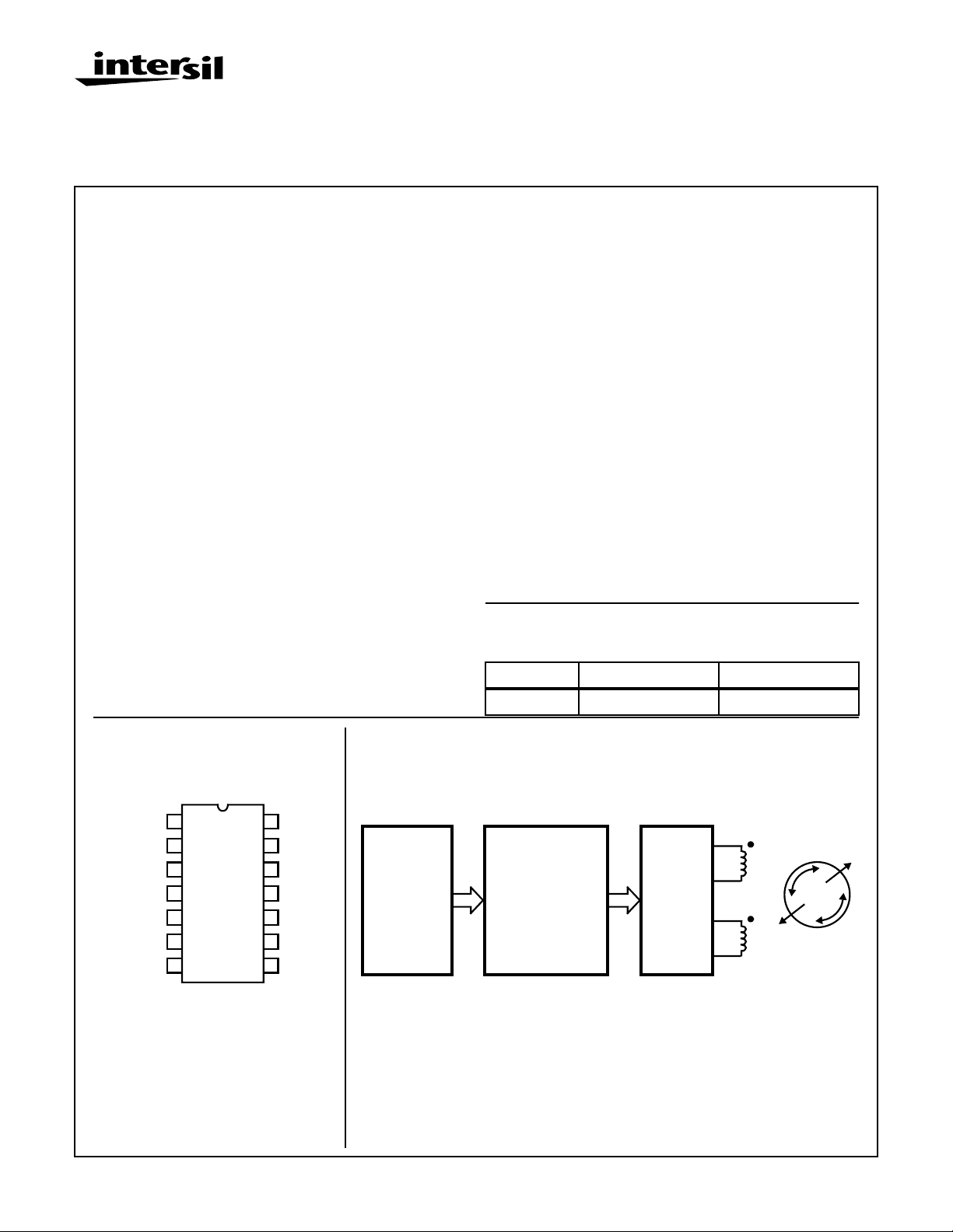
The CA3275 Dual Full Bridge Driver is intended for generalpurpose applications requiring Dual Full Bridge drive or
switching, including direction and pulse-width modulation for
position control. While all features of the IC may not be utilized or required, they would normally be used in instrumentation systems with quadrature coils, such as air-core
gauges, wherethe coils would bedriven atfrequencies ranging from 200Hz to 400Hz. The coils are wrapped at 90
angles for independent direction control. Coils wound in this
physical configuration are controlled by pulse width modulation, where each coil drive is a function of the sine or cosine
versus degrees of movement. The direction control is used
to change the direction of the current in the H-Driver coil.
The switch rate capability of the IC is typically 30kHz regardless of the inductive load. Over-current limiting is used to
limit short circuit current. Over-voltage protection (in the
range of 18V to 24V) causes the device to shut down the
output current drive.Thermal shutdown limits power dissipation on the chip.The CA3275 is supplied in a 14 lead dual-inline plastic package.
Ordering Information
o
• Slave Position Indicators
Pinout
CA3275 (PDIP)
TOP VIEW
V
CC
V
CC
PWMB
DIR B
V
CC
1
2
3
4
5
6
7
COIL A-
COIL B-
14
13
12
11
10
9
8
COIL A+
GND
PWMA
DIR A
GND
GND
COIL B+
Block Diagram
SENSOR &
CONVERTER
A/D, V/F, ETC
PART NO. TEMPERATURE PACKAGE
CA3275E -40oC to +85oC 14 Lead Plastic DIP
SIN
LA
MICROPROCESSOR
PHASE, DIRECTION
& PWM CONTROL
CA3275
DUAL-H
DRIVER
LB
ROTOR
COS
CAUTION: These devices are sensitive to electrostatic discharge; follow proper IC Handling Procedures.
1-888-INTERSIL or 321-724-7143
| Copyright © Intersil Corporation 1999
6-3
File Number
2159.3

Specifications CA3275
Absolute Maximum Ratings Thermal Information
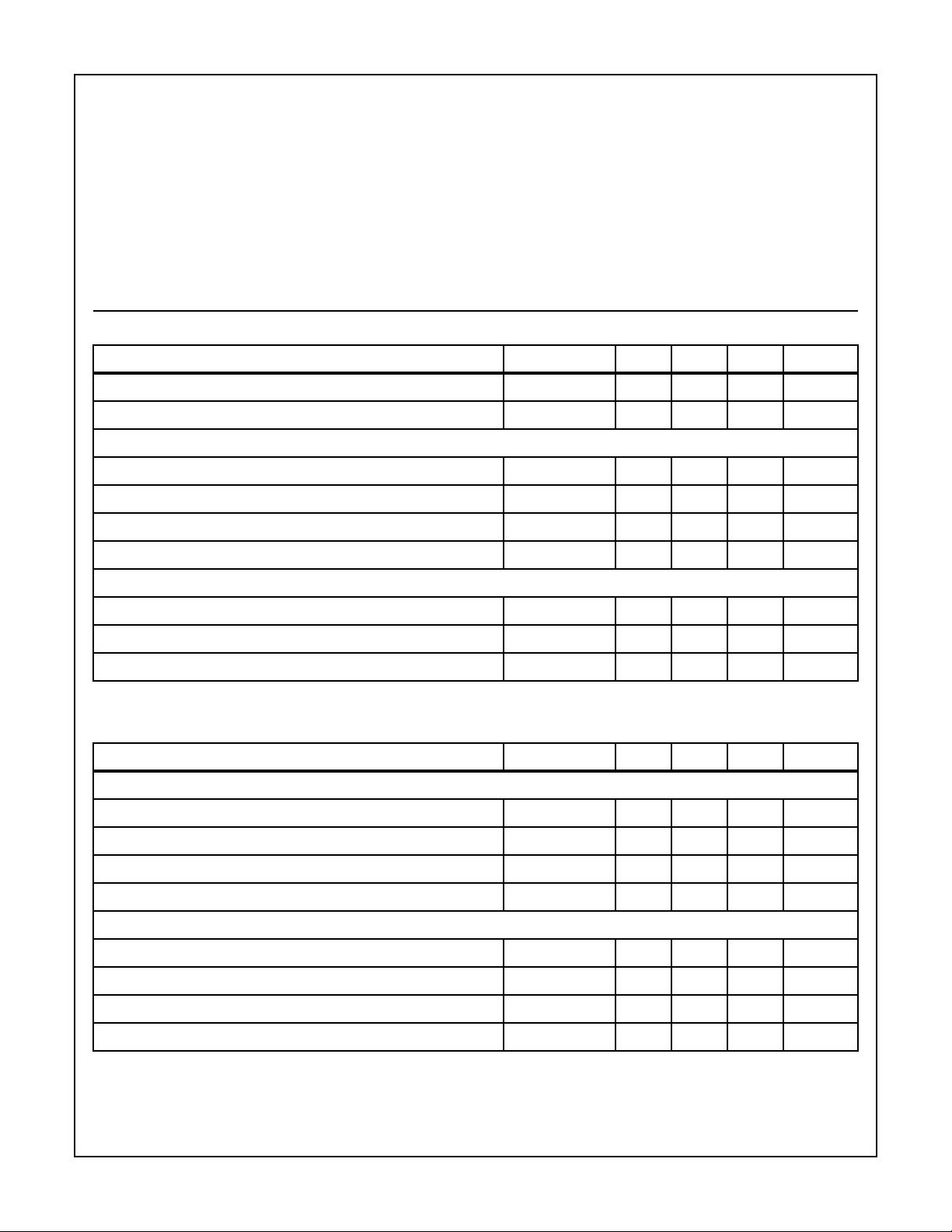
Operating VCC . . . . . . . . . . . . . . . . . . . . . . . . . . . . . . . . . . . . . . 16V
Transient VCC, 30 Seconds Maximum . . . . . . . . . . . . . . . . . . . . 24V
Peak VCC, 0.4 Seconds Maximum . . . . . . . . . . . . . . . . . . . . . . . 40V
Maximum Continuous Output Current,. . . . . . . . . . . . . . . . . . .±100mA
Each Drive
Maximum PWM Output Switching Current, . . . . . . . . . . . . . . .±150mA
Each Drive
CAUTION: Stresses above those listed in “Absolute Maximum Ratings” may cause permanent damage to the device. This is a stress only rating and operation
of the device at these or any other conditions above those indicated in the operational sections of this specification is not implied.
Thermal Resistance θ
JA
PDIP Package. . . . . . . . . . . . . . . . . . . . . . . . . . . . . . . . 100oC/W
Power Dissipation, P
D
Up to +70oC. . . . . . . . . . . . . . . . . . . . . . . . . . . . . . . . . . . . 800mW
Above +70oC. . . . . . . . . . . . . . . . . . .Derate Linearly at 10mW/oC
Ambient Temperature Range
Operating. . . . . . . . . . . . . . . . . . . . . . . . . . . . . . . .-40oC to +85oC
Storage . . . . . . . . . . . . . . . . . . . . . . . . . . . . . . . .-55oC to +150oC
Lead Temperature (During Soldering). . . . . . . . . . . . . . . . . . +265oC
At distance 1/16± 1/32" (1.59± 0.79mm) from case for 10s max
Electrical Specifications T
= -40oC to +85oC, VCC = 16V Unless Otherwise Specified
A
PARAMETERS SYMBOL MIN TYP MAX UNITS
Operating Supply Voltage Range V
Supply Current (Note 1) I
INPUT LEVELS
Logic Input, Low Voltage V
Logic Input, High Voltage V
Logic Input, Low Current, VIL = 0V I
Logic Input, High Current, VIH = 5V I
OUTPUT: RLA = RLB = 138Ω
Maximum Source Saturated Voltage V
Maximum Sink Saturated Voltage V
Differential V
Voltage, Both Outputs Saturated Diff - V
SAT
Switching Specifications
PARAMETERS SYMBOL MIN TYP MAX UNITS
CC
CC
IL
IH
IL
IH
- High - 1.2 1.75 V
SAT
- Low - 0.25 0.5 V
SAT
SAT
8 - 16 V
- 8 20 mA
- - 0.8 V
3.5 - - V
-10 - - µA
--10µA
- 10 100 mV
SOURCE CURRENT (See Figure 3)
Turn-Off Delay T
Fall Time T
Turn-On Time T
Rise Time T
SINK CURRENT (See Figure 4)
Turn-Off Delay T
Fall Time T
Turn-On Time T
Rise Time T
NOTE:
1. No load, PWMA = PWMB = 5V, DIR A = DIR B = 0V
6-4
SC-OFF
SC-F
SC-ON
SC-R
SK-OFF
SK-F
SK-ON
SK-R
--2 µs
- - 2.2 µs
--1 µs
- - 0.4 µs
- - 1.6 µs
- - 0.4 µs
- - 0.6 µs
- - 0.2 µs
 Loading...