Intersil Corporation CA3273 Datasheet

CA3273
April 1994
Features
• Equivalent High Pass P-N-P Transistor
• Current Limiting. . . . . . . . . . . . . . . . . . . . . .0.6A to 1.2A
• Over-Voltage Shutdown . . . . . . . . . . . . . . +25V to +40V
• Junction Temperature Thermal Limit. . . . . . . . .+150
• Equivalent Beta of 25. . . . . . . . . . . . . . . . . . 400mA/0.5V
• Internal Bandgap Voltage and Current Reference
Applications
• Fuel Pump Driver
• Relay Driver
• Solenoid Driver
• Stepper Motor Driver
• Remote Power Switch
• Logic Control Switch
High-Side Driver
Description
The CA3273 is a power IC equivalent of a P-N-P pass transistor operated as a high-side-driver current switch in either
the saturated (ON) or cutoff (OFF) modes. The CA3273
incorporates circuitry to protect the pass currents, excessive
input voltage, and thermal overstress. The high-side driver is
o
C
intended for general purpose, automotive and potentially
high-stress applications. If high-stress conditions exist, the
use of an external zener diode of 35V or less between supply and load terminals may be required to prevent damage
due to severe conditions (such as load dump, reverse battery and positive or negative transients). The CA3273 is
designed to withstand a nominal reverse-battery
(VBAT = 13V) condition without permanent damage to the
IC. The CA3273 is supplied in a modified 3-lead TO-202
plastic power package.
Ordering Information
PART
NUMBER
CA3273 -40oC to +85oC TO-202 Modified SIP
TEMPERATURE
RANGE PACKAGE
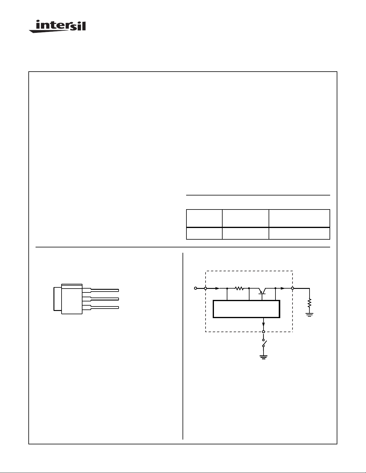
Pinout
CA3273 (SIP)
TOP VIEW
(3) VO (LOAD)
(2) V
(CONTROL)
SW
(1) V
(SUPPLY)
CC
Block Diagram
V
CC
PIN 1
I
CC
DRIVE AND LIMITING
CA3273
OUTPUT PASS
R
TRANSISTOR
S
CONTROL
PIN 2
V
SW
I
O
CONTROL
INPUT
V
O
PIN 3
R
L
LOAD
CAUTION: These devices are sensitive to electrostatic discharge; follow proper IC Handling Procedures.
407-727-9207
| Copyright © Intersil Corporation 1999
3-3
File Number
2113.4

Specifications CA3273
Absolute Maximum Ratings Thermal Information
Fault Max, Supply Voltage, VCC. . . . . . . . . . . . . . . . . . . . . . . . . 40V
Maximum Operating VCC:
At IO = 400mA (-40oC to +85oC Ambient) . . . . . . . . . . . . . . 16V
At IO = 600mA (-40oC to +25oC Ambient) . . . . . . . . . . . . . . 24V
Max. Positive Output Peak Pulse, VSW Open . . . . . . . . . .VCC+12V
Max. Operating Output Load Current . . . . . . . . . . . . . . . . . .600mA
Short Circuit Load Current, ISC . . . . . . . . . . . . . . . .Internal Limiting
Reverse Battery . . . . . . . . . . . . . . . . . . . . . . . . . . . . . . . . . . . . -13V
CAUTION: Stresses above those listed in “Absolute Maximum Ratings” may cause permanent damage to the device. This is a stress only rating and operation
of the device at these or any other conditions above those indicated in the operational sections of this specification is not implied.
Thermal Resistance θ
JA
Plastic SIP Package . . . . . . . . . . . . . . . . . . . . . . . . . . . +70oC/W
Maximum Power Dissipation, P
D
At +25oC Ambient, TA (Note 1). . . . . . . . . . . . . . . . . . . . . . .1.8W
Derate above +25oC (No Heat Sink) . . . . . . . . . . . . .14.3mW/oC
Maximum Junction Temperature, TJ (Note 2) . . . . . . . . . . . . 150oC
Ambient Operating Temperature Range . . . . . . . . .-40oC to +85oC
Storage Temperature Range. . . . . . . . . . . . . . . . . .-40oC to +150oC
Lead Temperature (Soldering 10s max) . . . . . . . . . . . . . . . .+265oC
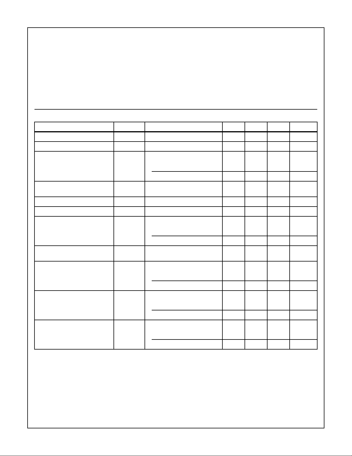
Electrical Specifications T
= -40oC to +85oC, Unless Otherwise Noted, See Block Diagram for Test Pin Reference
A
PARAMETERS SYMBOL TEST CONDITIONS MIN TYP MAX UNITS
Operating Voltage Range V
Saturation Voltage(VCC - VO)V
Operating Load R
CC
SAT
L
VCC Reference to V
SW
4 - 24 V
IO = -400mA, VSW = 0V, VCC = 16V - - 0.5 V
VSW = 0V (Switch ON)
TA = +85oC, VCC = 16V
40
-- Ω
TA = +25oC,VCC = 24V 40 Ω
Over-Voltage Shutdown Threshold V
CC(THD)
VSW = 0V, RL = 1kΩ, Increase V
CC,
25 33 40 V
(VO goes low)
Over-Current Limiting I
Over-Temperature Limiting T
Control Current, Switch ON I
O(LIM)
LIM
SW
VCC =16V, VSW = 1V (Switch ON) - - 1.2 A
- 150 -
VCC =16V, VSW = 0V
IO = 0mA - -15 - mA
IO = -400mA - -22 - mA
Control Current, Max. Load,
Switch ON
Max. Control Current,High and
Low V
CC
I
SW(MAX)
VCC = 24V, VSW = 0V,
- -33 - mA
IO = -600mA
RL = 40Ω, VSW = 1V
VCC = 24V -50 - - mA
VCC = 7V -50 - - mA
Min. Control Current, No Load,
Switch OFF
I
SW(NL)
VO = Open, (Switch OFF)
VCC = 24V,VSW = 23V -200 - +50 µA
VCC = 7V, VSW = 6V -200 - +50 µA
Output Current Leakage I
O(LEAK)
VO = 0V, VCC = 16V, (Switch OFF)
VSW =16V -100 - +100 µA
VSW =15V -100 - +100 µA
NOTES:
1. The calculation for dissipation and junction temperature rise due to dissipation is: PD=(VCC -VO)x I O+VCCxISW and
TJ=TA+PDx θJA where TJ is device junction temperature, TA is ambient temperature and θJA is the junction-to-ambient
thermal resistance.
2. Thermal limiting occurs at +150oC on the chip.
o
C
3-4
 Loading...