CA3262A, CA3262
August 1997
Features
• Independent Over-Current Limiting On Each Output
• Independent Over-Temperature Limiting On Each Output
• Output Drivers Capable of Switching 700mA Load
• Inputs Compatible With TTL or 5V CMOS Logic
• Suitable For Resistive, Lamp or Inductive Loads
• Power-Frame Package Construction For Good Heat
Dissipation
• Operating Temperature Ranges
- CA3262A . . . . . . . . . . . . . . . . . . . . . . . -40
- CA3262 . . . . . . . . . . . . . . . . . . . . . . . . . -40
o
C to 125oC
o
C to 85oC
Applications System Applications
• Solenoids • Automotive
• Relays • Appliances
• Lamps • Industrial Controls
• Steppers • Robotics
• Small Motors
• Displays
Ordering Information
TEMP.
PART NUMBER
CA3262E -40 to 85 16 Ld PDIP E16.3
CA3262AE -40 to 125 16 Ld PDIP E16.3
CA3262AQ -40 to 125 28 Ld PLCC N28.45
CA3262AM -40 to 125 24 Ld SOIC (W) M24.3
RANGE (oC) PACKAGE
PKG.
NO.
Quad-Gated, Inverting Power Drivers
Description
The CA3262 and CA3262A are used to interface low-level
logic to high current loads. Each Power Driver has four
inverting switches consisting of a non-inverting logic input
stage and an inverting low-side driver output stage. All inputs
are 5V TTL/CMOS logic compatible and have a common
Enable input. Each output device has independent current
limiting (I
over-load conditions. Steering diodes connected from each
output (in pairs) to the Clamp pins may be used in
conjunction with external zener diodes to protect the IC
against over-voltage tr ansients that result from inductive load
switching.
To allow for maximum heat transfer from the chip, all ground
pins on the DIP, PLCC and SOIC packages are directly
connected to the mounting pad of the chip. Integral heat
spreading lead frames directly connect the bond pads and
ground leads to conduct heat from the chip junction to the
PC Board for good heat dissipation.
The CA3262 and CA3262A can drive four incandescent
lamp loads without modulating their brilliance when the
“cold” lamps are energized. Outputs may be parallel
connected to drive high current loads. The maximum output
current of each output is determined by the over-current limiting threshold which is typically 1.2A but may be as low as
0.7A.
) and thermal limiting (T
LIM
) for protection from
LIM
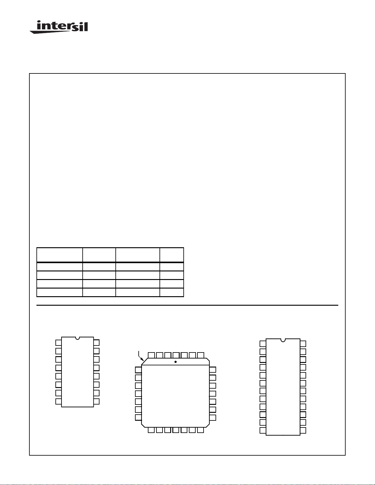
Pinouts
CA3262, CA3262A (PDIP)
TOP VIEW
1
OUT A
OUT B
GND
GND
OUT C
OUT D
2
3
4
5
6
7
8
CLAMP
CLAMP
16
15
14
13
12
11
10
9
IN A
IN B
ENABLE
GND
GND
V
CC
IN C
IN D
GND
GND
GND
GND
GND
GND
GND
CA3262A (PLCC)
TOP VIEW
INDEX
5
6
7
8
9
10
11
CLAMP
OUT B
12 13 14 15 16 17 18
OUT C
CLAMP
OUT A
NC
1234
NC
OUT D
IN A
IN D
1
IN B
IN C
ENABLE
262728
CC
V
CA3262A (SOIC)
TOP VIEW
PRELIMINARY
24
23
22
21
20
19
18
17
16
15
14
13
IN A
IN B
ENABLE
NC
GND
GND
GND
GND
NC
V
CC
IN C
IN D
NC
GND
GND
GND
GND
NC
1
2
3
4
5
6
7
8
9
10
11
12
OUT A
CLAMP
OUT B
GND
25
GND
24
GND
23
GND
22
21
GND
20
GND
19
GND
OUT C
CLAMP
OUT D
File Number 1836.6

CA3262A, CA3262
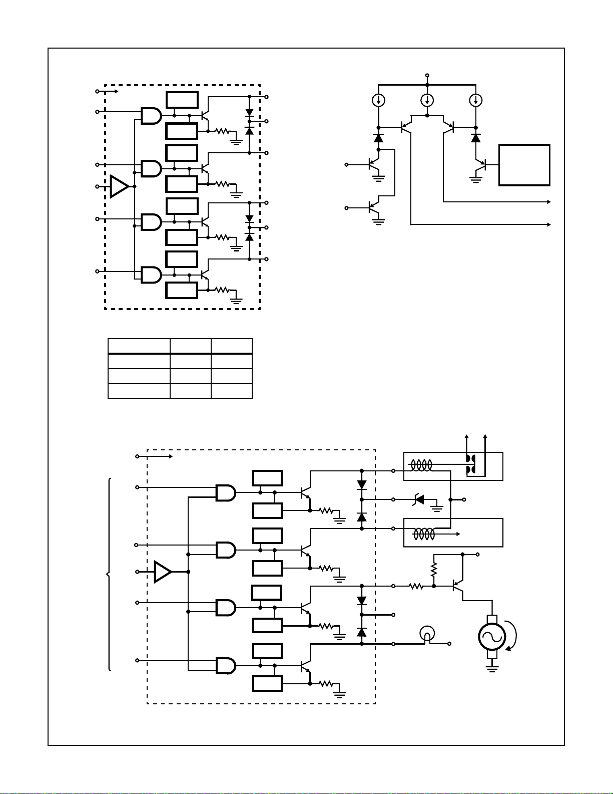
Functional Block Diagram
V
CC
IN D
IN C
ENABLE
IN B
IN A
V+
T
I
T
I
T
I
T
I
LIM
LIM
LIM
LIM
LIM
LIM
LIM
LIM
TRUTH TABLE (Each Output)
ENABLE IN OUT
HHL
HLH
LXH
H = High, L = Low, X = Don’t Care
OUT D
CLAMP
OUT C
OUT B
CLAMP
OUT A
V
CC
CONSTANT
CURRENT
SOURCES
REFERENCE
INPUT
ENABLE
TO SUBSEQUENT STAGES
VOLTAGE
FIGURE 1. CA3262A EQUIV ALENT SCHEMATIC OF ONE
INPUT STAGE
1.2V
TTL OR
CMOS
LOGIC
LEVEL
INPUTS
V
+5V P.S.
ENABLE
CC
IN D
IN C
IN B
IN A
V+
T
I
T
I
T
I
T
I
LIM
LIM
LIM
LIM
LIM
LIM
LIM
LIM
OUT D
CLAMP
OUT C
OUT B
CLAMP
OUT A
LAMP
RELAY
V
BATT
FIGURE 2. QUAD INVERTING POWER DRIVER (QDR) SHOWN WITH TYPICAL APPLICATION LOADS
V
BATT
SOLENOID
V
BATT
HIGH CURRENT
HIGH SIDE DR
MOTOR
2

CA3262A, CA3262
Absolute Maximum Ratings Thermal Information
Logic Supply Voltage, VCC. . . . . . . . . . . . . . . . . . . . . . . . . . . . . . 7V
Logic Input Voltage, VIN. . . . . . . . . . . . . . . . . . . . . . . . . . . . . . . 15V
Output Voltage, V
Output Sustaining Voltage, V
. . . . . . . . . . . . . . . . . . . . . . . . . . . . . . . . . 60V
CEX
CE(SUS)
. . . . . . . . . . . . . . . . . . . . 40V
Output Transient Current . . . . . . . . . . . . . . . . . . . . . . . . . . (Note 1)
Output Load Current. . . . . . . . . . . . . . . . . . . . . . . . . . . . . . (Note 2)
Operating Conditions
Temperature Range
CA3262AE, CA3262AQ, CA3262AM . . . . . . . . . . -40oC to 125oC
CA3262E. . . . . . . . . . . . . . . . . . . . . . . . . . . . . . . . . -40oC to 85oC
CAUTION: Stresses above those listed in “Absolute Maximum Ratings” may cause permanent damage to the device. This is a stress only rating and operation
of the device at these or any other conditions above those indicated in the operational sections of this specification is not implied.
Thermal Resistance (Typical, Note 3) θJA (oC/W)
For PC Mount Without Added Copper Ground Area
CA3262E (PDIP) . . . . . . . . . . . . . . . . . . . . . . . . . 60
CA3262AE (PDIP) . . . . . . . . . . . . . . . . . . . . . . . . 60
CA3262AQ (PLCC) . . . . . . . . . . . . . . . . . . . . . . . 45
CA3262AM (SOIC) . . . . . . . . . . . . . . . . . . . . . . . 60
For PC Mount With 2 sq. in. of Added Copper Ground Area
CA3262E (PDIP) . . . . . . . . . . . . . . . . . . . . . . . . . 40
CA3262AE (PDIP) . . . . . . . . . . . . . . . . . . . . . . . . 40
CA3262AQ (PLCC) . . . . . . . . . . . . . . . . . . . . . . . 36
CA3262AM (SOIC) . . . . . . . . . . . . . . . . . . . . . . . 36
See Maximum Power Dissipation vs Temperature curves, Figures
6A and 6B.
Maximum Junction Temperature . . . . . . . . . . . . . . . . . . . . . . . 150oC
Maximum Storage Temperature Range . . . . . . . . . .-65oC to 150oC
Maximum Lead Temperature (Soldering 10s) . . . . . . . . . . . . . 265oC
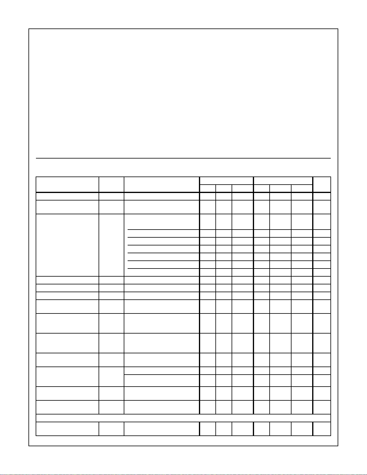
Electrical Specifications V
= 5.5V, TA = -40oC to 125oC for CA3262A and VCC = 5.5V, TA = -40oC to 85oC for CA3262
CC
Unless Otherwise Specified
PARAMETER SYMBOL TEST CONDITIONS
Output Leakage Current I
Output Sustaining
V
CEX
CE(SUS)
VCE = 60V, V
Note 5 40 - - 40 - - V
Voltage
Collector Emitter
Saturation Voltage
(See Figures 4B and 5B)
V
CE(SAT)VIN
= 2V, VCC = 4.75V
IC = 100mA - - 0.25 - 0.05 0.15 V
IC = 200mA - ----0.2V
IC = 300mA - ----0.25 V
IC = 400mA - - 0.4 - 0.2 0.3 V
IC = 500mA - ----0.4V
IC = 600mA - - 0.6 - - 0.5 V
IC = 700mA, TA = -40oC - - 0.6 - - 0.5 V
Input Low Voltage V
Input High Voltage V
Input Low Current I
Input High Current I
IL
IH
VIN = 0.8V - - 10 - 0.75 10 µA
IL
VIN = V
IH
ENABLE
IC = 600mA
Supply Current,
All Outputs ON,
(See Figures 4A and 5A)
Supply Current, All
Outputs OFF,
I
CC(ON)VIN
I
CC(OFF)
= 2V, V
I
= 250mA, I
OUTA
I
= 250mA, I
OUTC
VIN = 0V
(See Figures 4A and 5A)
Clamp Diode Leakage
Current
Clamp Diode Forward
Voltage,
(See Figures 4D and 5D)
Turn-On Delay,
t
PHL
I
R
VR = 60V
V
IF = 1A, VIN = 0V - - 1.7 - - 1.7 V
F
IF = 1.5A, VIN = 0V
, t
PLHIOUT
= 500mA - - 8 - - 8 µs
(See Figures 4C and 5C)
Over Current Limiting I
LIM
V
= 2V, VIN = 5.5V,
OUT
V
ENABLE
= 5.5V
DESIGN PARAMETERS
Over Temperature Limiting
T
LIM
(Junction Temperature)
ENABLE
= 5.5V,
ENABLE
CA3262 CA3262A
= 0.8V - - 100 - 0.6 50 µA
- - 0.8 - - 0.8 V
2--2- -V
- - 10 - - 10 µA
= 5.5V,
OUTB
OUTD
= 250mA,
= 250mA
- - 70 - (Note 4) 55 mA
- - 5 - (Note 4) 5 mA
- - 100 - - 50 µA
- - 2.1 - - 2.1 V
0.7 - (Note 1) 0.7 - (Note 1) A
- 155 - - 155 -
UNITSMIN TYP MAX MIN TYP MAX
o
C
3
 Loading...