Intersil Corporation CA3256 Datasheet

Semiconductor
CA3256
OBSOLETE PRODUCT
[ /Title
(CA32
56)
/Subject
(25MH
z,
BiMO
S Analog
Video
Switch
and
Amplifier)
/Autho
r ()
/Keywords
(Harris
Semiconductor,
4x1,
video
crosspoint
switch,
multiplexer
multiplexor,
cable
driver,
5x1,
moni
tor output,
adjustable
gain,
NO RECOMMENDED REPLACEMENT
January 1999
Call Central Applications 1-800-442-7747
or email: centapp@harris.com
Features
• 5 Multiplex Video Channels
- 1 Independent Channel
- 4 Channels with Enable
• 4 LED Channel Indicator Outputs
• Wideband Video Amplifier . . . . . . . .25MHz Unity Gain
• Adjustable Video Amplifier Gain
• High Signal-Drive Capability
Applications
• Video Multiplex Switch
•75Ω Video Amplifier/Line Driver
• Video Signal-Level Control
• Monitor Switching Control
• TV/CATV Audio/Video Switch
• Video Signal Adder/Fader Control
Part Number Information
TEMP.
PART NUMBER
CA3256E -40 to 85 18 Ld PDIP E18.3
CA3256M -40 to 85 20 Ld SOIC M20.3
RANGE (oC) PACKAGE
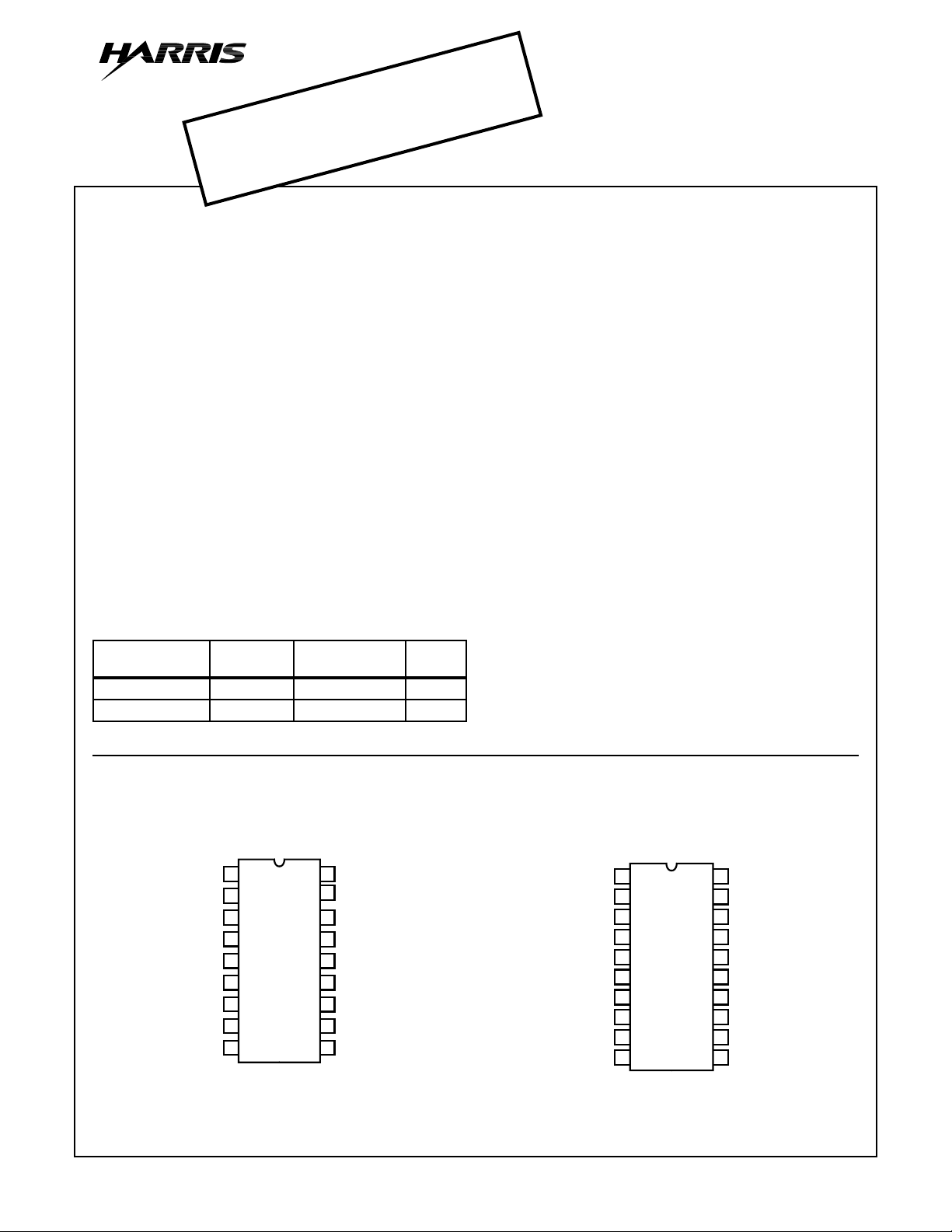
Pinouts
CA3256
(PDIP)
TOP VIEW
IN 3
LED 4
IN 4
GND
ENABLE
CONTROL C
FEEDBACK
AMP OUT
1
2
3
4
V- V+
5
6
7
8
9
18
CONTROL B
17
IN 2
16
CONTROL A
IN 1
15
14
13
IN/OUT 5
LED 1
12
LED 2
11
LED 3
10
PKG.
NO.
25MHz, BiMOS Analog
Video Switch and Amplifier
Description
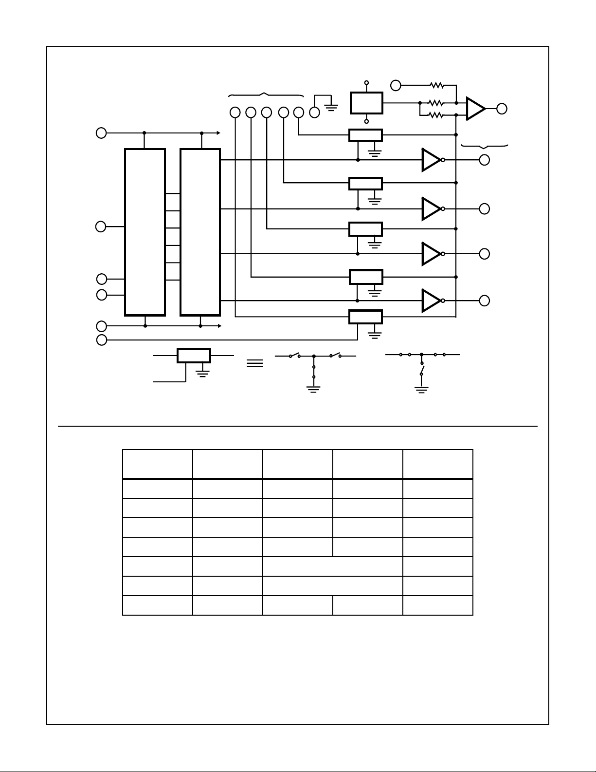
The CA3256 BiMOS analog video switch has five channels
of CMOS multiplex switching for general-purpose videosignal control. One of four CMOS channels may be selected
in parallel with channel 5. The CMOS switches are inputs to
the video amplifier but may be used in bilateral switching
between channels 1 to 4 and channel 5. The analog
switches of channels 1 to 4 are digitally controlled with logic
level conversion and binary decoding to select 1 of 4
channels. The enable function controls channels 1 to 4 but
does not affect channel 5. LED output drivers are selected
with the channel 1-to-4 switch selection to indicate the ONchannel. Channel 5 may be used as a monitor output for
data or signal information on channels 1 to 4. The
transmission gate switches shown in the block diagram of
the CA3256 are configured in a “T” design to minimize
feedthrough. When the switch is off, the shunt or center of
the “T” is grounded.
The amplifier has high input impedance to minimize the R
transmission gate insertion loss. The amplifier output impedance is typically 5Ω in a complementary symmetry output.
The amplifier can directly drive a nominal 75Ω coaxial cable
to provide line-to-line video switching. The gain of the amplifier is programmable by different feedback resistor values
between pins 8 and 9. Compensation may also be used
between these pins for an optimally flat frequency response.
An internal regulated 5V bias reference with temperature
compensation permits stable direct-coupled output drive and
minimizes DC offset during signal switching.
CA3256
(SOIC)
TOP VIEW
IN3
LED4
IN4
GND
ENABLE
CONTROL C
FEEDBACK
AMP OUT
LED3
1
2
3
4
V-
5
6
7
8
9
10
CONTROL B
20
IN2
19
CONTROL A
18
NC
17
IN1
16
V+
15
IN/OUT5
14
NC
13
12
LED1
LED2
11
ON
CAUTION: These devices are sensitive to electrostatic discharge. Users should follow proper IC Handling Procedures.
Copyright
© Harris Corporation 1999
8-1
File Number 1769.5

Block Diagram
V+
14
CA3256
IN/OUT
5 4 3 2 1
13 3 1
FEED BACK
V+
BIAS
1517
4
REG
V-
TG
TG
8
1K
10K
10K
AMPLIFIER
OUTPUT
-
+
LED DRIVER
OUTPUTS
12
CHANNEL 1
9
ENABLE
6
A
16
18
B
V-
5
C
7
LOGIC
LEVEL
CONV.
IN OUT
SW
CONTROL
Switch Control Logic
CHANNEL
NUMBER C A B ENABLE
10001
BINARY
TO
1 OF 4
WITH
ENABLE
TG
IN OUT
SW
OPEN
(DIP PIN OUT)
TG
TG
TG
IN OUT
SW
CLOSED
11
CHANNEL 2
10
CHANNEL 3
2
CHANNEL 4
20011
30101
40111
5 + (1-4) (Note) 1 Channel 1-4 1
5 1 Channel 5 Only 0
None 0 X X 0
NOTE: For Maximum Video Bandwidth, Use Single Channel Selections
8-2

CA3256
Absolute Maximum Ratings Thermal Information
DC Supply Voltage Range (V+ to V-) . . . . . . . . . . . . . . . . . . . . . 18V
Control Input Voltage Range, All Inputs . . . . . . . . . . . . . . . . V+ to V-
Signal Input Voltage Range, Channel 1-5 . . . . . . . . . . . . . . . .3V
Amplifier Output Current. . . . . . . . . . . . . . . . . . . . . . . . . . . . . .30mA
DC LED Sink Current . . . . . . . . . . . . . . . . . . . . . . . . . . . . . . . .30mA
Operating Conditions
Temperature Range . . . . . . . . . . . . . . . . . . . . . . . . . . -40oC to 85oC
CAUTION: Stresses above those listed in “Absolute Maximum Ratings” may cause permanent damage to the device. This is a stress only rating and operation
of the device at these or any other conditions above those indicated in the operational sections of this specification is not implied.
NOTE:
1. θJA is measured with the component mounted on an evaluation PC board in free air.
Thermal Resistance (Typical, Note 1) θJA (oC/W)
PDIP Package. . . . . . . . . . . . . . . . . . . . . . . . . . . . . 70
P-P
SOIC Package. . . . . . . . . . . . . . . . . . . . . . . . . . . . . 75
Maximum Junction Temperature (Die). . . . . . . . . . . . . . . . . . . .175oC
Maximum Junction Temperature (Plastic Package) . . . . . . . . 150oC
Maximum Storage Temperature Range . . . . . . . . . -65oC to 150oC
Maximum Lead Temperature (Soldering 10s) . . . . . . . . . . . . . 300oC
(SOIC - Lead Tips Only)
Electrical Specifications T
= 25oC, V+ = 12V; V- = GND
A
PARAMETER SYMBOL TYPICAL VALUES UNITS
Power Supply Voltage V+ to V- 10 to 17 V
Power Supply Current I
CC
20 mA
SWITCH AMPLIFIER
Open Loop Gain A
OL
Programmable Gain, FB Adjustment Range - -0.8 A
-35dB
OL
Full Power Bandwidth - 10 MHz
Unity Gain Bandwidth, 1kΩ, 7pF Compensation - 25 MHz
Insertion Loss -0.8 - dB
Signal Feedthrough, 5MHz -66 - dB
Input Impedance Z
Output Impedance Z
Maximum Input Voltage V
Maximum Output Voltage, Clipped V
O(MAX)
IN
OUT
I(MAX)
-10kΩ
-5Ω
3 2.5 V
-7V
Reference Bias Output Voltage (V8 - V-) - 5 V
dB
P-P
P-P
Differential Gain - 1 %
Differential Phase - 1 Degree
Off Isolation, Channel to Channel, ZIN = 75Ω -66 - dB
LLC Switch Turn On/Off Time Delay - 0.5 µs
Maximum LED Sink Current - 30 mA
Typical Output Source Current - 16 mA
Channel Control Switch A, B, C and EN Threshold
V
TH
Approximately (V+ - V-)/2 V
(Notes 2, 3)
CAUTION: Connect the V- power supply voltage before or during the V+ turn-on.
NOTES:
2. Threshold value is referenced to GND.
3. VTH is restricted by the equation, VTH < V+ -1.
8-3

CA3256
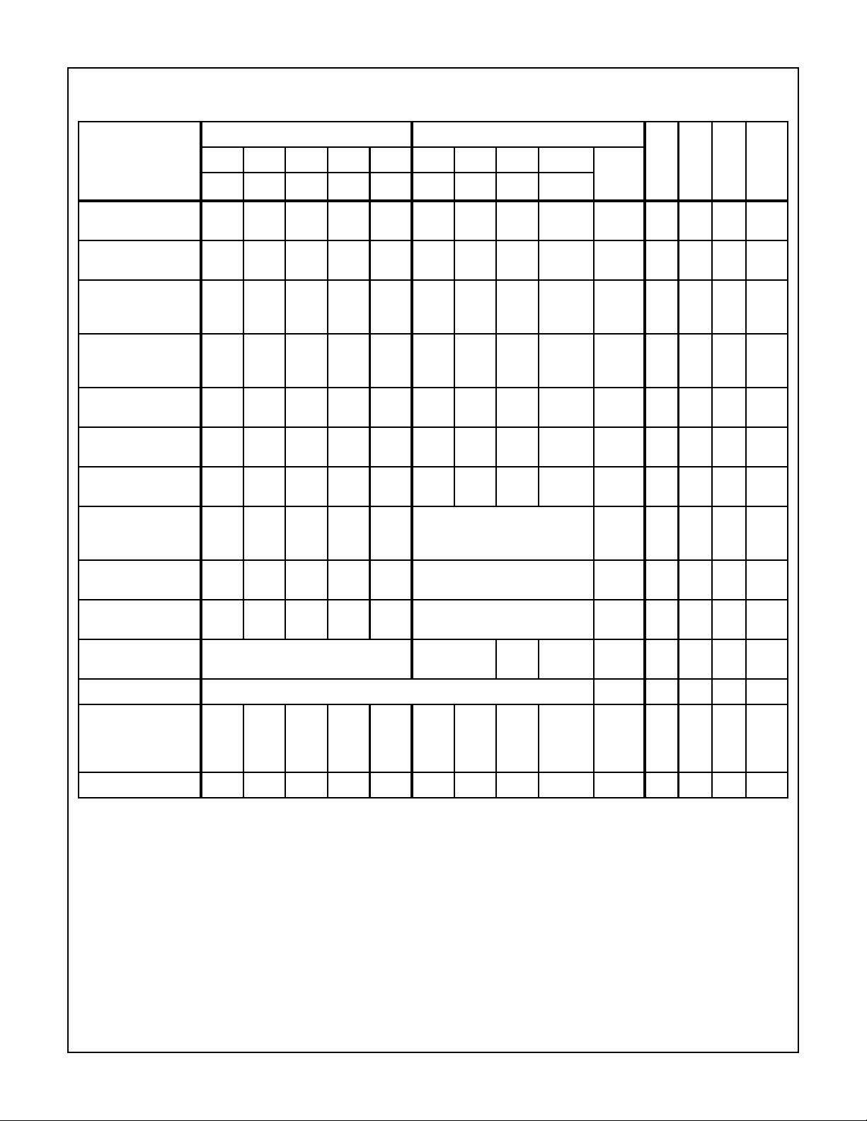
Electrical Specifications T
CH 1 CH 2 CH 3 CH 4 CH 5 A B C ENABLE NOTE 6
PARAMETERS
Supply Current,
V
= 0V
LED
Dual Supply Current
V+ = +7V, V- = -5V
Amplifier Output
Voltage, Open Loop
V
= 0V
LED
Amplifier Output
Voltage , Closed Loop,
V
= 0V
LED
I
OUT (MAX)
(Source)
Open Loop
I
OUT (MAX)
(Sink)
Open Loop
Input Leakage
Channel 1-5
0V 0V 0V 0V 0V 3V 3V 3V 3V 14 10 16 22 mA
0V 0V 0V 0V 0V 0V 0V 0V 7V 14/5 10 20 26 mA
0V 0V 0V 0V 0V 3V 3V 3V 3V 9 6 8.5 10 V
0V 0V 0V 0V 0V 3V 3V 3V 3V 9 4.8 5.1 5.4 V
0V 0V 0V 0V 0V 3V 3V 3V 3V 9
0V 0V 0V 0V 0V 3V 3V 3V 3V 9
3V 3V 3V 3V 3V 3V 3V 3V 3V 1, 3, 15,17-15 5 15 nA
= 25oC, V+ = 12V, V
A
= 12V , V- = GND, Pin 4 = GND , F eedback Switch Closed, V
LED
(See Figure 1), Unless Otherwise Specified
INPUTS CHANNEL SWITCH CONTROL
TEST
PIN#PIN 15 PIN 17 PIN 1 PIN 3 PIN 13 PIN 16 PIN 18 PIN 7 PIN 6
Note 4
Note 5
HIGH
= 9V , V
LOW
= 3V
MIN TYP MAX UNITS
- -70 -25 mA
10 16 - mA
Channel Control
Input A, B, C,
Enable Leakage
LED Off Voltage, V
0V 0V 0V 0V 0V Measure at 3V, 9V each;
Enable and Channel
Switching Control Inputs
0V 0V 0V 0V 0V Select Channel 0-5 2, 10,
OFF
6, 7, 16,18-20 10 20 nA
11.97 11.99 - V
11, 12
LED On Voltage, V
0V 0V 0V 0V 0V Select Channel 0-5 2, 10,
ON
- 0.1 0.3 V
11, 12
Switch Resistance,
R
DS
RDS Match Calculation: (Max RDS - Min RDS)/Min R
Amplifier Output
±100µA Input Each Switch,
Channel 1-4 + 5
Select Channel
1-4
9V 9V 0.8 1.1 1.4 kΩ
DS
- - 3.6 5 %
0V 0V 0V 0V 0V 0V 0V 0V 7V 9 -100 45 100 mV
Offset, VO, Feedback
Switch Closed
V+ = +7V, V- = -5V
Closed Loop Gain 3V 0V 0V 0V 0V 3V 3V 3V 9V 9 -0.5 -0.1 0.5 dB
NOTES:
4. V
5. V
OUT
OUT
= +7V.
= +3V.
6. DIP Pinout.
8-4
 Loading...