Intersil Corporation CA3252 Datasheet

CA3252
March 1998
Features
• Four 600mA Non-Inverting Power Output Drivers
• 50V and 1A Maximum Rated Power Output Drivers
•V
CE(SUS)
Capability . . . . . . . . . . . . . . . . . . . . . . . . .35V
• Inputs Compatible With TTL or 5V CMOS Logic
• Suitable For Resistive, Lamp or Inductive Loads
• Inductive Clamps on Each Output
• High Dissipation Power-Frame Package
• Operating Temperature Ranges. . . . . . -40
o
Applications
• Solenoids
• Relays
• Lamps
• Steppers
• Small Motors
• Displays
System Applications
• Automotive
C to 105oC
Quad Gated Non-Inverting Power Driver
Description
The CA3252 is used to interface low-level logic to high current loads. Each Power Driver has four inverting switches
consisting of an inverting logic input stage and an inverting
low-side driver output stage. All inputs are 5V TTL/CMOS
logic compatible and have a common Enable input. On-chip
steering diodes are connected from each output (in pairs) to
the CLAMP pins (in pairs) which may be used in conjunction
with external zener diodes to protect the IC against over-voltage transients that result from inductive load switching. The
CA3252 may be used in a variety of automotive and industrial control applications to drive relays, solenoids, lamps and
small motors.
To allow for maximum heat transfer from the chip, all ground
pins on the DIP and SOIC packages are directly connected
to the mounting pad of the chip. Integral heat spreading lead
frames directly connect the bond pad and ground leads for
good heat dissipation. In a typical application, the package is
mounted on a copper PC Board. By increasing copper
ground area on the PC Board, more heat is conducted away
from the ground leads. The junction-to-ambient thermal
resistances may be reduced to less than 40
approximately two square inches of copper area.
Ordering Information
PART
NUMBER TEMP. (oC) PACKAGE PKG. NO.
o
C/W with
• Appliances
• Industrial Controls
CA3252E -40 to 105 16 Ld PDIP E16.3
CA3252M -40 to 105 20 Ld SOIC M20.3
• Robotics
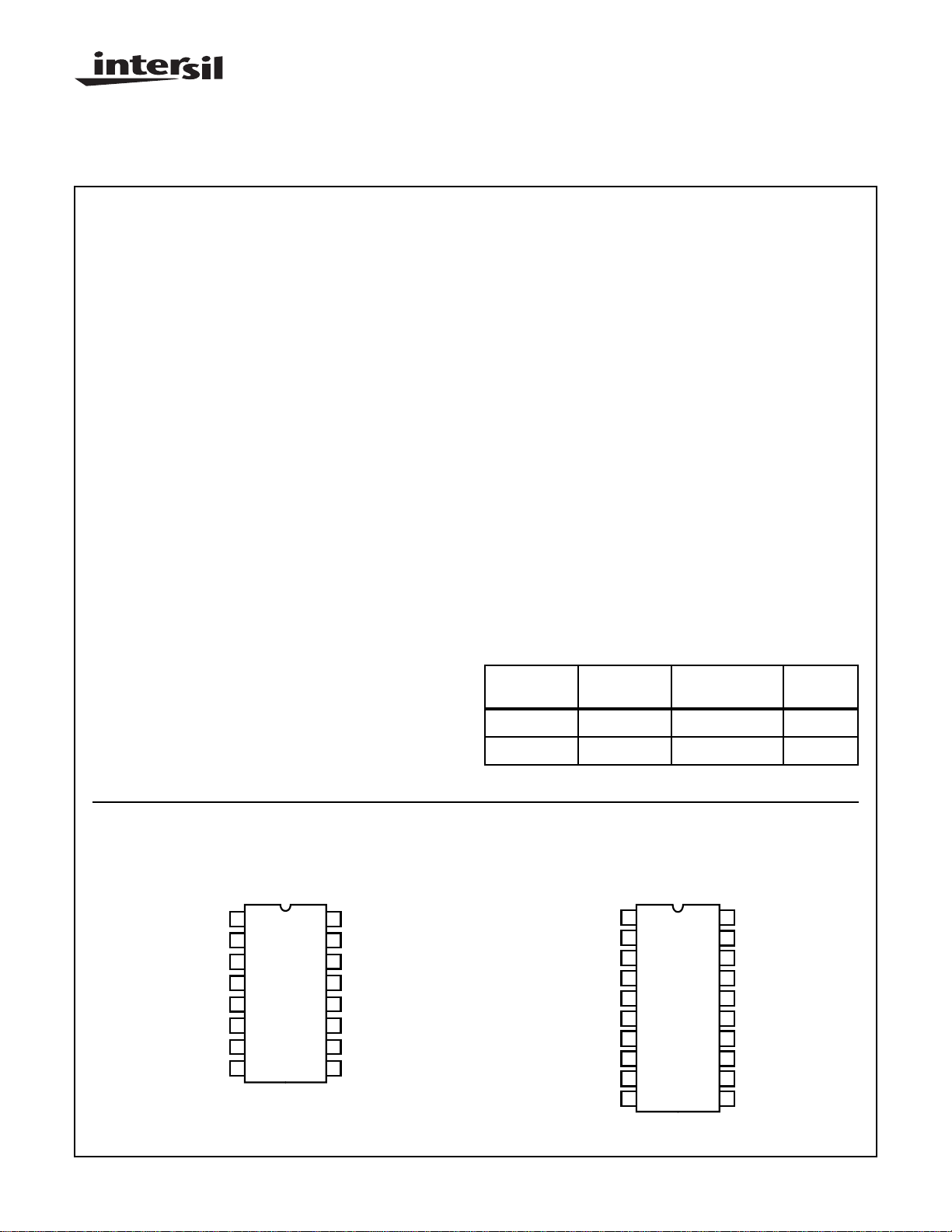
Pinouts
CA3252E
(PDIP)
TOP VIEW
1
OUT A
OUT B
GND
GND
OUT C
OUT D
2
3
4
5
6
7
8
| Copyright © Intersil Corporation 1999
CLAMP AB
CLAMP CD
CAUTION: These devices are sensitive to electrostatic discharge; follow proper IC Handling Procedures.
http://www.intersil.com or 407-727-9207
16
15
14
13
12
11
10
9
IN A
IN B
ENABLE
GND
GND
V
CC
IN C
IN D
1
CLAMP AB
CLAMP CD
NC
NC
OUT B
GND
GND
OUT C
NC
NC
CA3252M
(SOIC)
TOP VIEW
1
2
3
4
5
6
7
8
9
10
OUT A
20
IN A
19
INB
18
ENABLE
17
GND
16
GND
15
V
14
CC
IN C
13
12
IN D
11
OUT D
File Number 1542.2

Functional Block Diagram
CA3252
V
CC
IN D
IN C
V
IN D
IN C
GND
GND
ENABLE
IN B
IN A
V+
CC
V+
OUT D
CLAMP
OUT C
OUT D
CLAMP
OUT C
GND
GND
OUT B
CLAMP
OUT A
RELAY
V
BATT
SOLENOID
GND GND
ENABLE
IN B
IN A
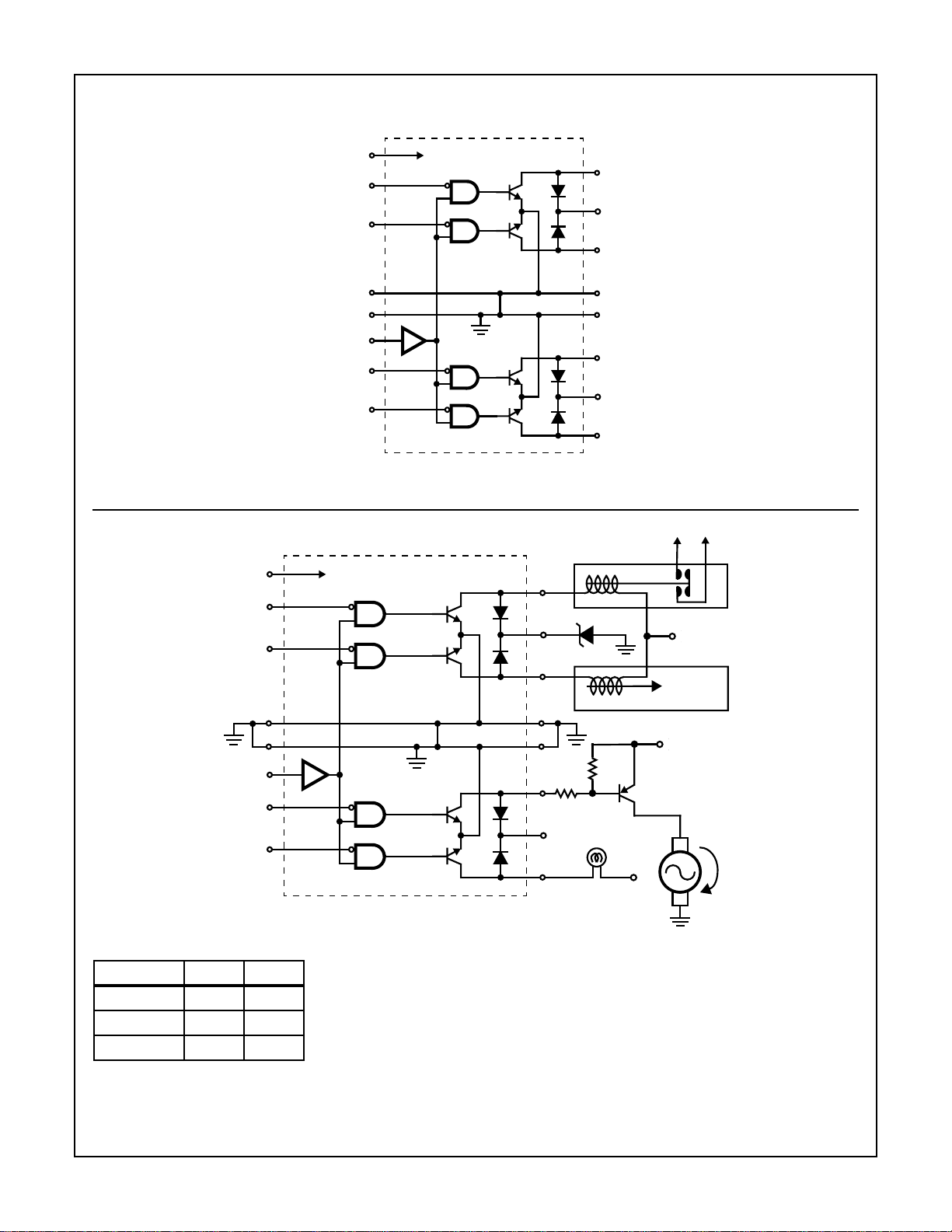
TRUTH TABLE (Each Output)
ENABLE IN OUT
HLL
HHH
LXH
H = High, L = Low, X = Don’t Care
FIGURE 1. CA3252 QUAD NON-INVERTING POWER DRIVER SHOWN WITH TYPICAL APPLICATION LOADS
OUT B
CLAMP
OUT A
LAMP
V
HIGH CURRENT
HIGH SIDE DR
V
BATT
BATT
MOTOR
2
 Loading...