

Intersil Corporation CA3242 Datasheet
August 1998
CA3242
Quad-Gated Inverting Power Driver For
Interfacing Low-Level Logic to High Current Load
Features
• Driven Outputs Capable of Switching 600mA Load
Currents Without Spurious Changes in Output State
• Inputs Compatible with TTL or 5V CMOS Logic
• Suitable for Resistive or Inductive Loads
• Output Overload Protection
• Power-Frame Construction for Good Heat Dissipation
Applications
• Relays
• Solenoids
• AC and DC Motors
• Heaters
• Incandescent Displays
• Vacuum Fluorescent Displays
Ordering Information
TEMPERATURE
PART NUMBER
CA3242E -40oC to +105oC 16 Lead Plastic DIP
RANGE PACKAGE
Description
The CA3242 quad-gated inverting power driver contains four
gate switches for interfacing low-level logic to inductive and
resistive loads such as: relays, solenoids, AC and DC
motors, heaters, incandescent displays, and vacuum fluorescent displays.
Output overload protection is provided when the load current
(approximately 1.2A) causes the output V
above 1.3V. A built-in time delay , nominally 25µs, is provided
during output turn-on as output drops from V
output will be shut down by its protection network without
affecting the other outputs. The corresponding Input or
Enable must be toggled to reset the output protection circuit.
Steering diodes in the outputs in conjunction with external
zener diodes protect the IC against voltage transients due to
switching inductive loads.
To allow for maximum heat transfer from the chip, the four
center leads are directly connected to the die mounting pad.
In free air, junction-to-air thermal resistance (R
(typical). This coefficient can be lowered by suitable design
of the PC board to which the CA3242 is soldered.
(sat) to rise
CE
to V
DD
SAT
) is 60oC/W
θJA
. That
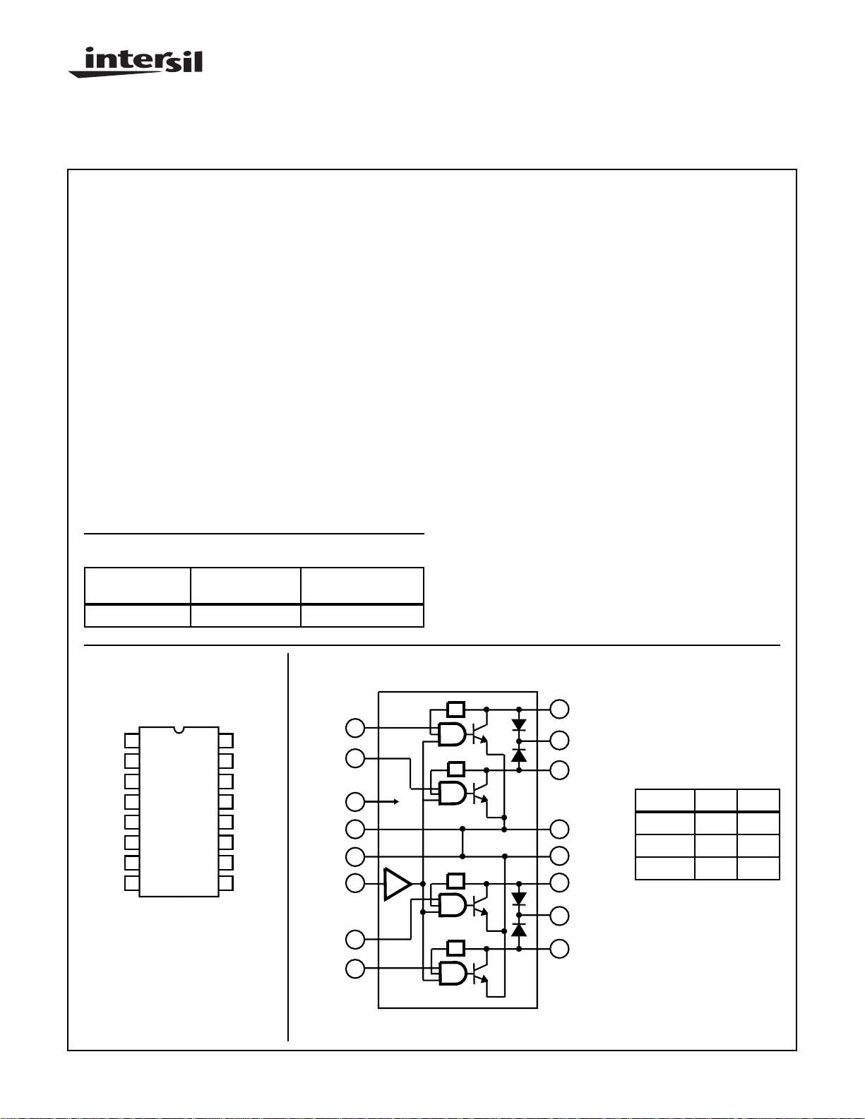
Pinout
CA3242 (PDIP)
TOP VIEW
1
OUT A
OUT B
GND
GND
OUT C
OUT D
2
3
4
5
6
7
8
| Copyright © Intersil Corporation 1999
CLAMP
CLAMP
CAUTION: These devices are sensitive to electrostatic discharge; follow proper IC Handling Procedures.
407-727-9207
16
15
14
13
12
11
10
9
IN A
IN B
ENABLE
GND
GND
V
CC
INC
IND
Block Diagram
9
IN D
10
IN C
11
VCC
12
GND
GND
13
IN B
IN A
14
15
16
ENABLE
P
P
P
P
2-3
8
7
6
5
4
3
2
1
OUT D
CLAMP
OUT C
GND
GND
OUT B
CLAMP
OUT A
TRUTH TABLE
ENABLE IN OUT
HHL
HLH
LXH
File Number 1561.2
 Loading...