CA3240, CA3240A
Data Sheet August 2001 File Number 1050.5
Dual, 4.5MHz, BiMO S Operational Amplifie r
with MOSFET Input/Bipolar Output
The CA3240Aand CA3240 are dual versions of the popular
CA3140 seriesintegratedcircuit operationalamplifiers. They
combine the advantagesof MOS and bipolar transistors on
the same monolithic chip. The gate-protected MOSFET
(PMOS) input transistorsprovide high input impedance and
a wide common-mode input voltage range (typically to 0.5V
below the negative supply rail). The bipolar output
transistorsallow a wide output voltage swing and provide a
high output current capability.
TheCA3240AandCA3240arecompatiblewiththeindustry
standard 1458 operationalamplifi e rsinsimilarpa ckages.The
offsetnullfeatureis availableonly when thesetypes are supplied
inthe14leadPDIPpackage(E1suffix).
Ordering Information
TEMP.
PART NUMBER
RANGE (oC) PACKAGE
CA3240AE -40 to 85 8 Ld PDIP E8.3
CA3240AE1 -40to85 14LdPDIP E14.3
CA3240E -40 to 85 8Ld PDIP E8.3
PKG.
NO.
Features
• Dual Version of CA3140
• Internally Compensated
• MOSFET Input Stage
- Very High Input Impedance (Z
- Very Low Input Current (I
- Wide Common-Mode Input Voltage R ange (V
)1.5TΩ (Typ)
IN
) 10pA (Typ) at ±15V
I
ICR
): Can
Be Swung 0.5V Below Negative Supply Voltage Rail
• Directly Replaces Industry Type 741 in Most Applications
Applications
• Ground Referenced Single Amplifiers in Automobile and
Portable Instrumentation
• Sample and Hold Amplifiers
• Long Duration Timers/Multivibrators ( MicrosecondsMinutes-Hours)
• PhotocurrentInstrumentation
• Intrusion Alarm System • ActiveFilters
• Comparators • Function Generators
• Instrumentation Amplifiers • Power Supplies
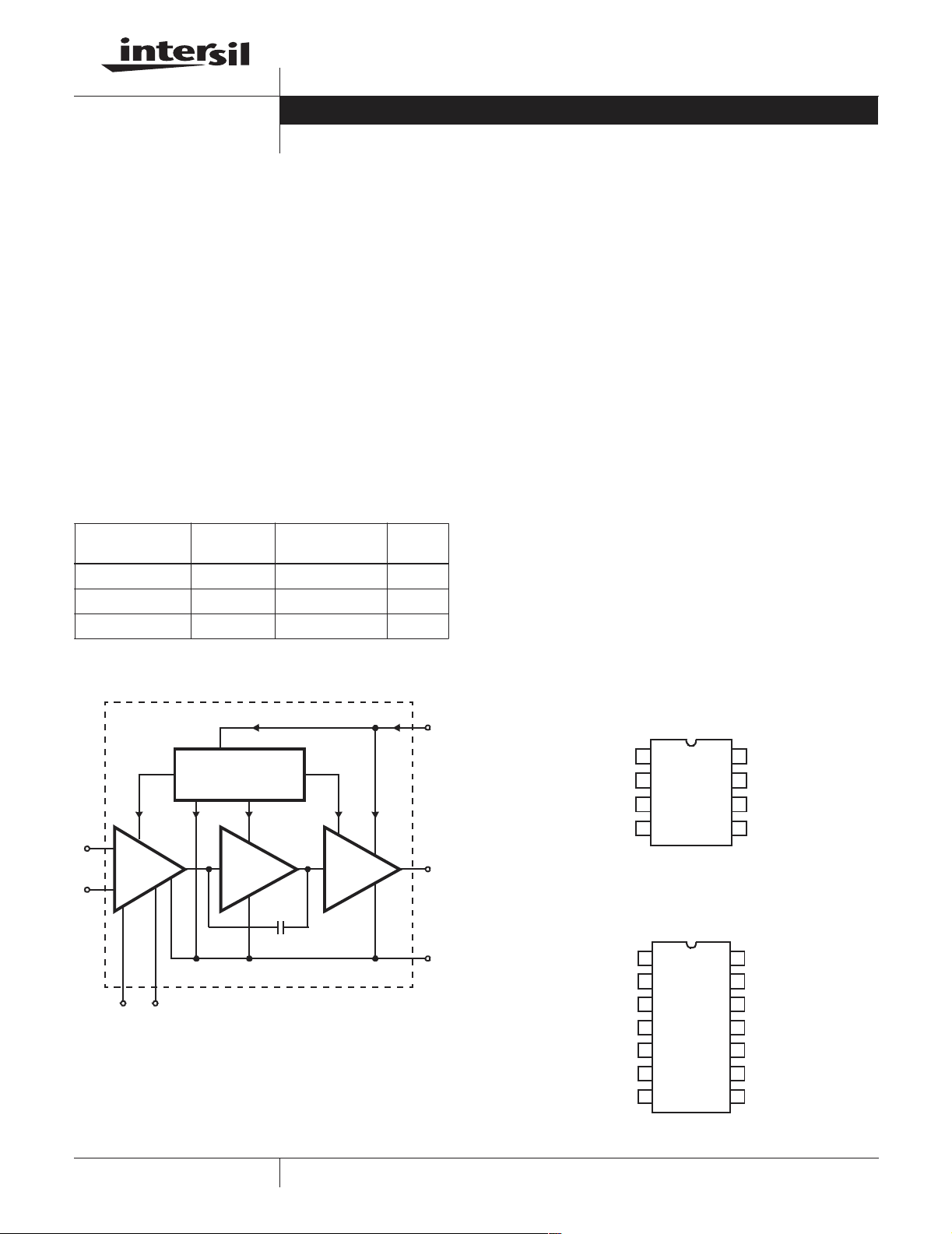
Functional Diagram
2mA 4mA
BIAS CIRCUIT
CURRENT SOURCES
AND REGULATOR
+
IN-
PUT
A ≈ 10
-
OFFSET NULL
NOTE: Only available with 14 lead DIP (E1 Suffix).
A ≈ 10,000
12pF
A ≈ 1
C
1
Pinouts
CA3240, CA3240A (PDIP)
V+
OUTPUT (A)
INV.
INPUT (A)
NON-INV.
2mA1.6mA 2µA200µA200µA
OUT-
PUT
V-
INPUT (A)
INV.
INPUT (A)
NON-INV.
INPUT (A)
OFFSET
NULL (A)
OFFSET
NULL (B)
NON - INV.
INPUT (B)
INV.
INPUT (B)
† Pins 9 and 13 internally connected through approximately 3Ω.
TOP VIEW
1
2
3
4
V-
CA3240A (PDIP)
TOP VIEW
1
2
3
4
V-
5
6
7
8
V+
OUTPUT
7
INV.
6
INPUT (B)
NON-INV.
5
INPUT (B)
OFFSET
14
NULL ( A)
V+†
13
OUTPUT (A)
12
NC
11
OUTPUT (B)
10
V+
9
OFFSET
8
NULL ( B)
†
1
1-888-INTERSIL or 321-724-7143
CAUTION: These devices are sensitive to electrostatic discharge; follow proper IC Handling Procedures.
| Intersil and Design is a trademarkof Intersil AmericasInc. | Copyright © Intersil Americas Inc. 2001
CA3240, CA3240A
Absolute Maximum Rati ng s Thermal Information
SupplyVoltage(BetweenV+andV-)..................... 36V
DifferentialInputVoltage............................... 8V
InputVoltage.........................(V++8V)to(V--0.5V)
InputCurrent.......................................1mA
OutputShortCircuitDuration(Note1)................ Indefinite
Operating Conditions
TemperatureRange..........................-40oCto85oC
VoltageRange.....................4Vto36Vor±2V to ±18V
CAUTION: Stresses above those listed in “Absolute Maximum Ratings” may cause permanent damage to the device. This is a stress only rating and operationofthe
device at these or any other conditions above those indicated in the operational sections of this specification is not implied.
NOTES:
1. Short circuit may be applied to ground or to either supply. Temperatures and/or supply voltages must be limited to keep dissipation within maximum rating.
is measuredwith the component mountedon an evaluation PC board in free air.
2. θ
JA
Thermal Resistance (Typical, Note 2)
θ
JA
(oC/W)
8LeadPDIPPackage....................... 100
14LeadPDIPPackage...................... 100
MaximumJunction Temperature (PlasticPackage) . . . . . . . 150
MaximumStorageTemperatureRange..........-65
o
Cto150oC
Maximum Lead Temperature (Soldering 10s) . . . . . . . . . . . . 300
o
C
o
C
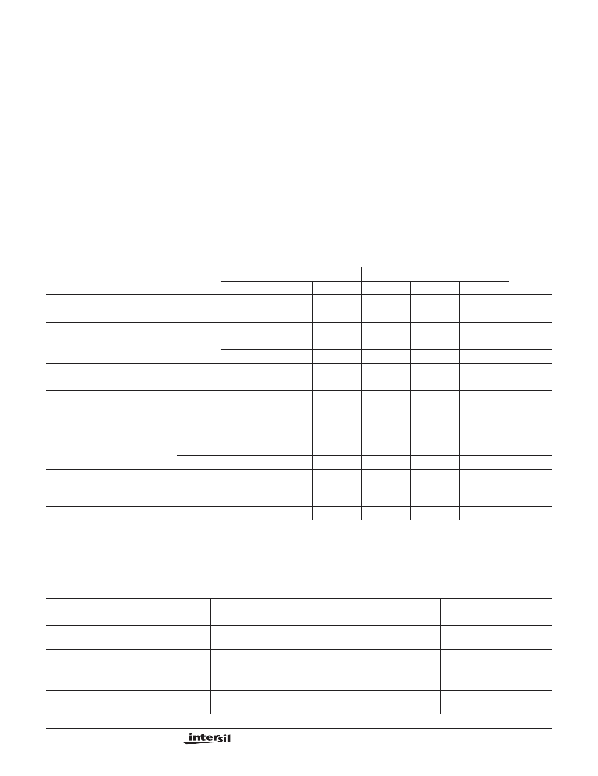
Electrical Specifications ForEquipment Design, V
PARAMETER SYMBOL
Input Offset Voltage V
Input Offset Current I
Input Current I
Large-SignalVoltage Gain
(See Figures 13, 28) (Note 3)
CommonModeRejection
Ratio(SeeFigure18)
Common Mode Input VoltageRange
(See Figure 25)
Power Supply Rejection Ratio
(See Figure 20)
(∆V
Maximum Output Voltage (Note 4)
(See Figures 24, 25)
Maximum Output Voltage (Note 5) V
Total SupplyCurrent
(See Figure 16) For Both Amps
Total Device Dissipation P
NOTES:
3. At V
4. At R
=26V
O
=2kΩ.
L
5. At V+ = 5V, V- = GND, I
, +12V, -14V and RL=2kΩ.
P-P
=200µA.
SINK
IO
IO
I
A
OL
CMRR - 32 320 - 32 320 µV/V
V
ICR
PSRR
/∆V±)
IO
+ 12 13 - 12 13 - V
V
OM
- -14 -14.4 - -14 -14.4 - V
V
OM
OM-
I+ - 8 12 - 8 12 mA
D
-515- 2 5mV
- 0.5 30 - 0.5 20 pA
- 10 50 - 10 40 pA
20 100 - 20 100 - kV/V
86 100 - 86 100 - dB
70 90 - 70 90 - dB
-15 -15.5 to
- 100 150 - 100 150 µV/V
76 80 - 76 80 - dB
0.4 0.13 - 0.4 0.13 - V
- 240 360 - 240 360 mW
SUPPLY
= ±15V,TA=25oC, Unless Otherwise Specified
CA3240 CA3240A
11 -15 -15.5 to
+12.5
UNITSMIN TYP MAX MIN TYP MAX
12 V
+12.5
Electrical Specifications For EquipmentDesign, V
PARAMETER SYMBOL TEST CONDITIONS
Input Offset Voltage Adjustment Resistor (E1
PackageOnly)
Input Resistance R
Input Capacitance C
Output Resistance R
Equivalent WidebandInput NoiseVoltage
(See Figure 2)
2
I
I
O
e
N
= ±15V, TA=25oC, Unless Otherwise Specified
SUPPLY
TYPICAL VALUES
UNITSCA3240A CA3240
TypicalValueof Resistor Between Terminals4and 3(5)
or Between 4 and 14(8) to Adjust Maximum V
IO
18 4.7 kΩ
1.5 1.5 TΩ
44pF
60 60 Ω
BW = 140kHz, RS=1MΩ 48 48 µV
CA3240, CA3240A
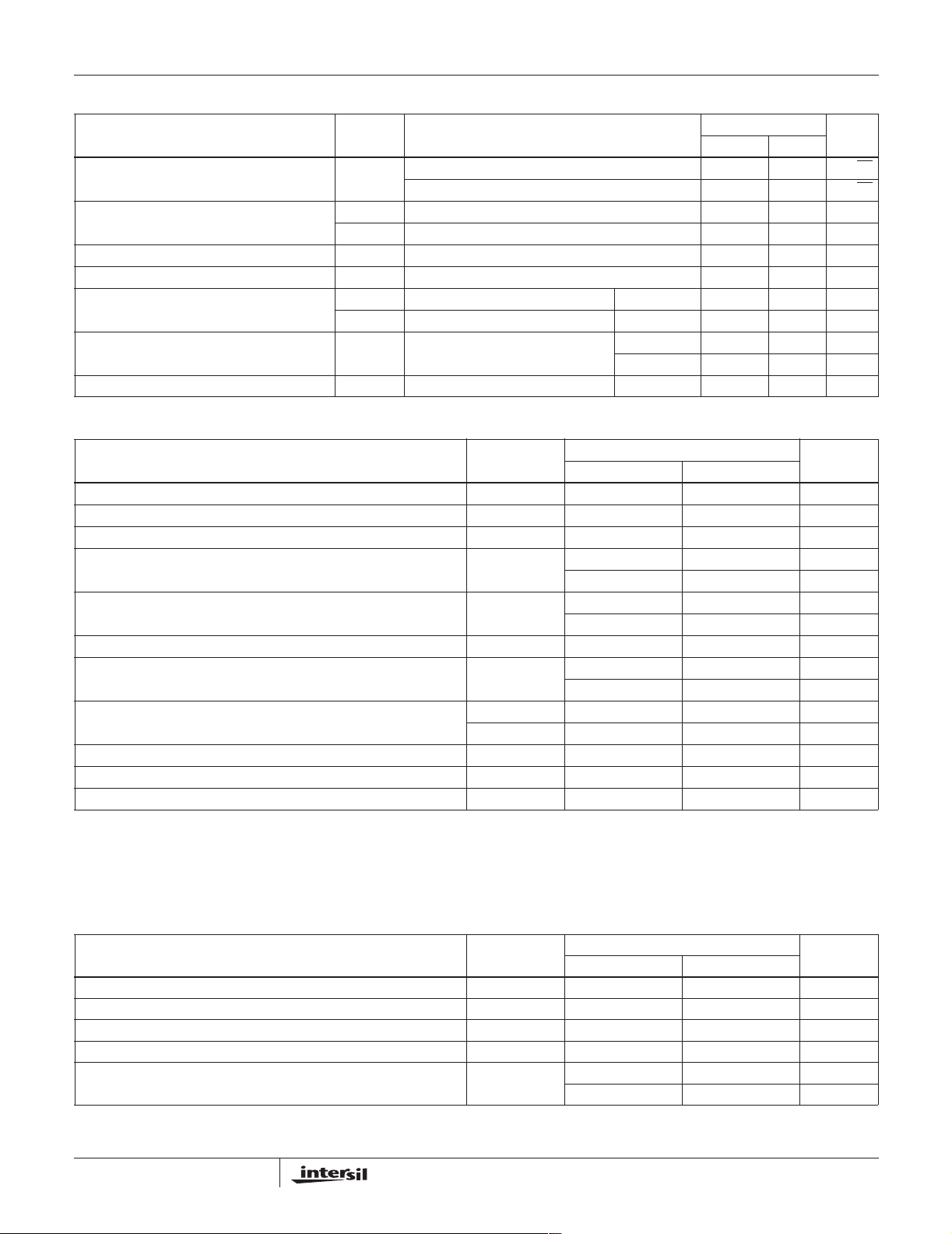
Electrical Specifications For EquipmentDesign, V
= ±15V, TA=25oC, Unless Otherwise Specified (Continued)
SUPPLY
TYPICAL VALUES
PARAMETER SYMBOL TEST CONDITIONS
Equivalent Input Noise V oltage
(See Figure 19)
e
f=1kHz,RS=100Ω 40 40 nV/√Hz
N
f=10kHz,RS=100Ω 12 12 nV/√Hz
UNITSCA3240A CA3240
Short-CircuitCurrent to Opposite Supply IOM+Source 40 40 mA
-Sink 11 11 mA
I
OM
Gain BandwidthProduct (See Figures 14, 28) f
T
4.5 4.5 MHz
Slew Rate (See Figure 15) SR 9 9 V/µs
Transient Response (See Figure 1) t
Settling Timeat 10V
(See Figure 26) t
P-P
OS R
RL=2kΩ,CL= 100pF Rise Time 0.08 0.08 µs
r
=2kΩ,CL= 100pF Overshoot 10 10 %
L
AV=+1,RL=2kΩ,CL= 100pF,
S
Voltage Follower
To 1mV 4.5 4.5 µs
To 10mV 1.4 1.4 µs
Crosstalk (See Figure 23) f = 1kHz 120 120 dB
Electrical Specifications For Equipment Design, at V
= ±15V ,TA= -40 to 85oC, Unles sOtherwise Specified
SUPPLY
TYPICAL VALUES
PARAMETER SYMBOL
Input Offset Voltage |V
Input Offset Current (Note 8) |I
Input Current (Note 8) I
Large Signal Voltage Gain (See Figures 13, 28), (Note 6) A
|3 10mV
IO
|32 32pA
IO
I
OL
640 640 pA
63 63 kV/V
UNITSCA3240A CA3240
96 96 dB
Common Mode Rejection Ratio (See Figure 18) CMRR 32 32 µV/V
90 90 dB
Common Mode Input VoltageRange (See Figure 25) V
ICR
Power Supply Rejection Ratio (See Figure 20) PSRR
/∆V±)
(∆V
IO
Maximum Output Voltage (Note 7) (See Figures 24, 25) V
OM
V
OM
+12.4 12.4 V
- -14.2 -14.2 V
-15to+12.3 -15to+12.3 V
150 150 µV/V
76 76 dB
SupplyCurrent (SeeFigure 16) Total For Both Amps I+ 8.4 8.4 mA
Total Device Dissipation P
Temperature Coefficient of Input Offset Voltage ∆V
D
/∆T15 15µV/oC
IO
252 252 mW
NOTES:
6. At V
7. At R
8. At T
=26V
O
=2kΩ.
L
=85oC.
A
, +12V, -14V and RL=2kΩ.
P-P
Electrical Specifications For EquipmentDesign, at V+ = 5V, V- = 0V, T
PARAMETER SYMBOL
Input Offset Voltage |V
Input Offset Current |I
Input Current I
Input Resistance R
Large Signal Voltage Gain (See Figures 13, 28) A
3
=25oC, Unless Otherwise Specified
A
TYPICAL VALUES
UNITSCA3240A CA3240
|2 5mV
IO
|0.1 0.1pA
IO
I
IN
OL
22pA
11TΩ
100 100 kV/V
100 100 dB
CA3240, CA3240A
Electrical Specifications For EquipmentDesign, at V+ = 5V, V- = 0V, T
=25oC, Unless Otherwise Specified (Continued)
A
TYPICAL VALUES
PARAMETER SYMBOL
UNITSCA3240A CA3240
Common-Mode Rejection Ratio CMRR 32 32 µV/V
90 90 dB
Common-Mode InputVoltage Range (See Figure 25) V
ICR
-0.5 -0.5 V
2.6 2.6 V
Power Supply Rejection Ratio PSRR 31.6 31.6 µV/V
90 90 dB
Maximum Output Voltage (See Figures 24, 25) V
MaximumOutput Current Source I
Sink I
+3 3 V
OM
-0.3 0.3V
V
OM
+20 20mA
OM
-1 1mA
OM
Slew Rate (See Figure 15) SR 7 7 V/µs
Gain Bandwidth Product (See Figure 14) f
T
4.5 4.5 MHz
SupplyCurrent (SeeFigure 16) I+ 4 4 mA
Device Dissipation P
D
20 20 mW
Test Circuits and Waveforms
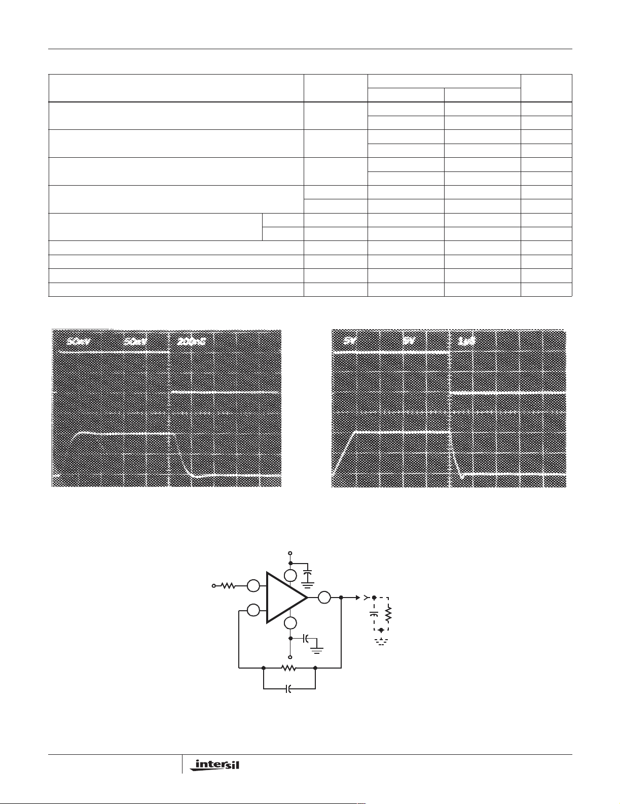
50mV/Div .,200ns/Div.
Top Trace:Input, Bottom Trace: Output
Top Trace:Input, Bottom Trace: Output
5V/Div., 1µs/Div.
FIGURE 1A. SMALL SIGNAL RESPONSE FIGURE 1B. LARGE SIGNAL RESPONSE
+15V
10kΩ
+
CA3240
-
-15V
2kΩ
0.05µF
0.1µF
0.1µF
BW (-3dB) = 4.5MHz
SR = 9V/µs
SIMULATED
100pF
LOAD
2kΩ
FIGURE 1C. TEST CIRCUIT
FIGURE 1. SPLIT-SUPPLY VOLTAGE FOLLOWER TEST CIRCUIT AND ASSOCIATED WAVEFORMS
4
CA3240, CA3240A
Test Circuits and Waveforms (Continued)
R
S
1MΩ
+15V
+
CA3240
-
0.01µF
30.1kΩ
NOISE
VOLT AGE
OUTPUT
BW (-3dB) = 140kHz
TOTAL NOISE VOLTAGE
(REFERRED TO INPUT) = 48µV(TYP)
FIGURE 2. TEST CIRCUIT AMPLIFIER (30dB GAIN) USED FOR WIDEBAND NOISE MEASUREMENT
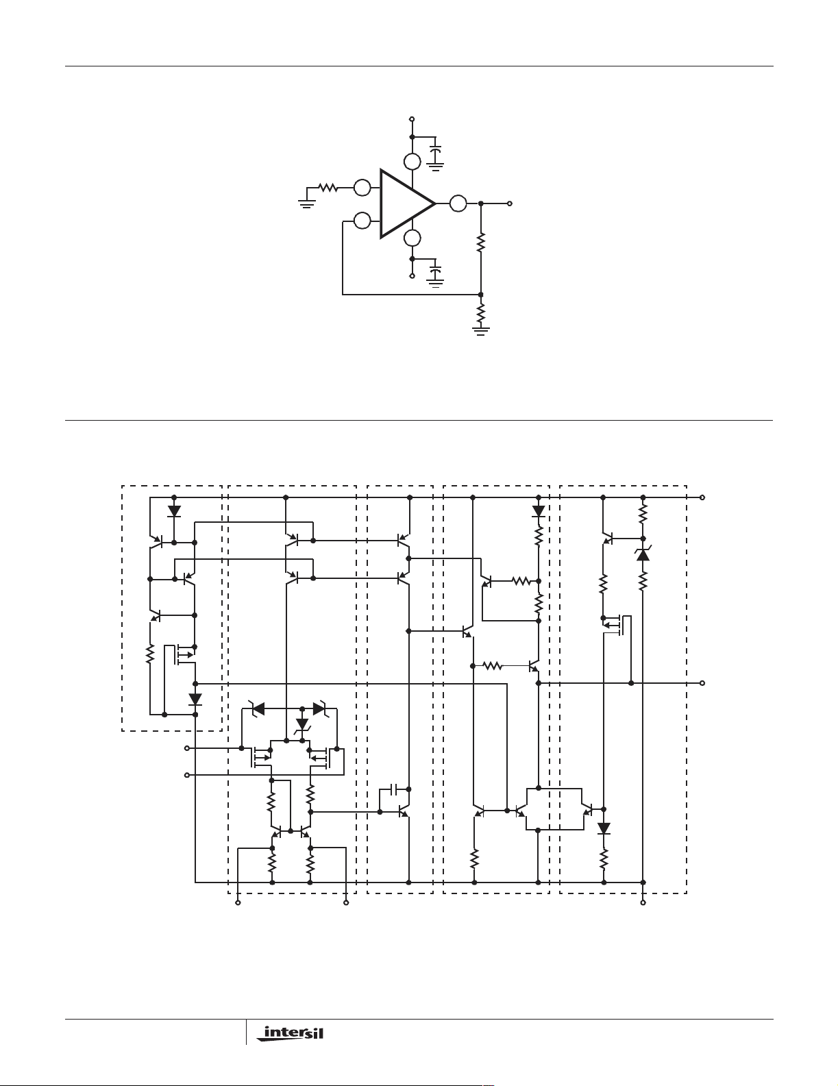
Schematic Diagram (One Amplifier of Two)
BIAS CIRCUIT INPUT STAGE SECOND STAGE OUTPUT STAGE D YNAMIC CURRENT SINK
D
1
Q
2
Q
5
D
3
D
4
R
8K
Q
1
Q
6
Q
7
1
Q
8
D
2
-15V
0.01µF
1kΩ
V+
D
7
R
Q
3
Q
4
Q
17
R
1K
9
50Ω
R
10
Q
19
1K
R
11
20Ω
8
Q
18
R
12K
R
13
15K
Q
20
D
8
R
12
Q
14
20K
21
OUTPUT
INVERTING
NON-INVERTING
INPUT
INPUT
-
Q
+
R
2
500Ω
Q
11
R
4
500Ω
OFFSET NULL (NOTE 9)
NOTES:
9. Onlyavailablewith14LeadDIP(E1Suffix).
10. All r esistance valuesare in ohms.
5
D
5
Q
10
9
R
3
500Ω
Q
12
R
5
500Ω
C
12pF
1
Q
Q
13
14
R
6
50Ω
Q
Q
16
15
D
R
7
30Ω
6
V-
