Intersil Corporation CA3193A, CA3193 Datasheet

1
Semiconductor
January 1998
CA3193, CA3193A
1.2MHz, BiCMOS
Precision Operational Amplifiers
CAUTION: These devices are sensitive to electrostatic discharge. Users should follow proper IC Handling Procedures.
Copyright
© Harris Corporation 1999
File Number 1249.4
Features
•Low V
IO
- CA3193A . . . . . . . . . . . . . . . . . . . . . . . . . .200µV (Max)
- CA3193 . . . . . . . . . . . . . . . . . . . . . . . . . . .500µV (Max)
•Low∆V
IO
/∆T
- CA3193A . . . . . . . . . . . . . . . . . . . . . . . . .3µV/
o
C (Max)
- CA3193 . . . . . . . . . . . . . . . . . . . . . . . . . .5µV/
o
C (Max)
•Low I
IO
and I
I
•Low∆IIO/∆T: CA3193. . . . . . . . . . . . . . .150pA/oC (Max)
•Low∆I
I
/∆T: CA3193 . . . . . . . . . . . . . . . . 3.7nA/oC (Max)
Applications
• Thermocouple Preamplifiers
• Strain Gauge Bridge Amplifiers
• Summing Amplifiers
• Differential Amplifiers
• Bilateral Current Sources
• Log Amplifiers
• Differential Voltmeters
• Precision Voltage References
• Active Filters
• Buffers
• Integrators
• Sample-and-Hold Circuits
• Low Frequency Filters
Description
The CA3193A and CA3193 are ultra-stable, precision
instrumentation, operational amplifiers that employ both
PMOS and bipolar transistors on a single monolithic chip.
The CA3193A and CA3193 amplifiers are internally phase
compensated and provide a gain bandwidth product of
1.2MHz. They are pin compatible with the industry 741
series and many other IC op amps, and may be used as
replacements for 741 series types in most applications.
The CA3193A and CA3193 can also be used as functional
replacements for op amp types 725, 108A, OP-5, OP-7,
LM11 and LM714 in many applications where nulling is not
employed. Because of their low offset voltage and low offset
voltage vs temperature coefficient the CA3193A and
CA3193 amplifiers have a wider range of applications than
most op amps and are particularly well suited for use as
thermocouple amplifiers, high gain filters, buffer, strain
gauge bridge amplifiers and precision voltage references.
The two types in the CA3193 series are functionally
identical. The CA3193A and CA3193 operate from supply
voltages of ±3.5V to ±18V.
Pinout
CA3193
(PDIP)
TOP VIEW
Part Number Information
PART NUMBER
TEMP.
RANGE (oC) PACKAGE
PKG.
NO.
CA3193AE -25 to 85 8 Ld PDIP E8.3
CA3193E 0 to 70 8 Ld PDIP E8.3
OFFSET NULL
INV. INPUT
NON-INV. INPUT
V-
1
2
3
4
8
7
6
5
NC
V+
OUTPUT
OFFSET NULL
-
+
t
le
3193,
193A)
ject
Hz,
OS
ision
ational
lifiers)
hor ()
words
ris
icon-
ational
ifier,
cost op
t bias
nt, pre-
n,
strial
ercial
era-
unity
stable,
ge
ack
FOR A POSSIBLE SUBSTITUTE PRODUCT
call Central Applications 1-800-442-7747
or email: centapp@harris.com
OBSOLETE PRODUCT

2
Absolute Maximum Ratings Thermal Information
DC Supply Voltage. . . . . . . . . . . . . . . . . . . . . . . . . . . . . . . . . . . . . . ±18V
Differential Input Voltage. . . . . . . . . . . . . . . . . . . . . . . . . . . . . . . . 5V
DC Input Voltage . . . . . . . . . . . . . . . . . . . . . . . . . . . . . . . (V+ -4), V-
Input Current. . . . . . . . . . . . . . . . . . . . . . . . . . . . . . . . . . . . . . . .1mA
Output Short Circuit Duration (Note 2) . . . . . . . . . . . . . . . . Indefinite
Operating Conditions
Temperature Range
CA3193A. . . . . . . . . . . . . . . . . . . . . . . . . . . . . . . . . -25oC to 85oC
CA3193. . . . . . . . . . . . . . . . . . . . . . . . . . . . . . . . . . . .0oC to 70oC
Thermal Resistance (Typical, Note 1) θJA (oC/W) θJC (oC/W)
PDIP Package. . . . . . . . . . . . . . . . . . . 100 N/A
Maximum Junction Temperature (Plastic Package) . . . . . . . . 150oC
Maximum Storage Temperature Range . . . . . . . . . .-65oC to 150oC
Maximum Lead Temperature (Soldering 10s). . . . . . . . . . . . .300oC
CAUTION: Stresses above those listed in “Absolute Maximum Ratings” may cause permanent damage to the device. This is a stress only rating and operation
of the device at these or any other conditions above those indicated in the operational sections of this specification is not implied.
NOTES:
1. θJA is measured with the component mounted on an evaluation PC board in free air.
2. Short circuit may be applied to ground or to either supply.
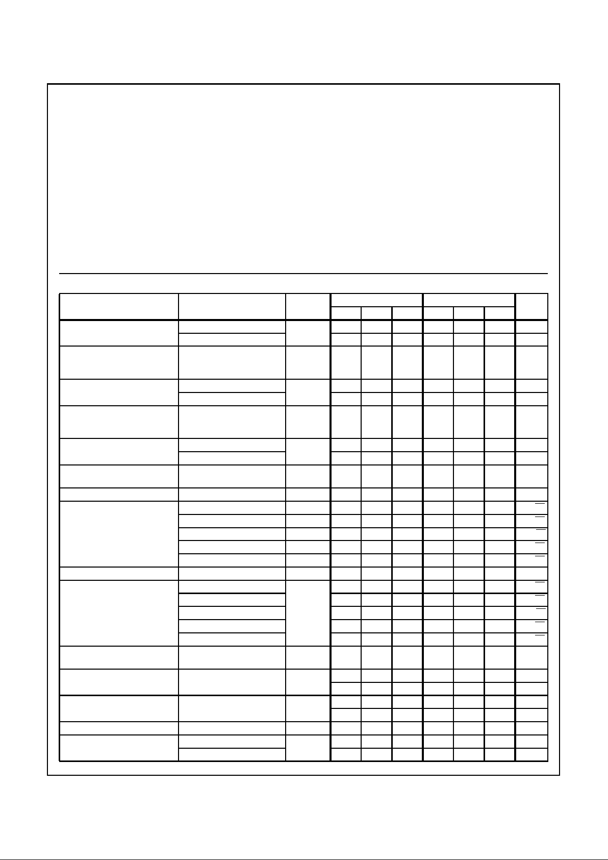
Electrical Specifications T
A
= 25oC, V
SUPPLY
= ±15V, Unless Otherwise Specified
PARAMETER
TEST
CONDITIONS SYMBOL
CA3193 CA3193A
UNITSMIN TYP MAX MIN TYP MAX
Input Offset Voltage V
IO
25oCV
IO
- 300 500 - 140 200 µV
T
MAX
- - 725 - - 380 µV
Input Offset Voltage Temperature
Coefficient (Over Specified Temperature Range for Each Device)
∆V
IO
/∆T- 1 5 - 1 3µV/oC
Input Offset Current 25
o
CI
IO
- 5 10 - 3 5 nA
T
MAX
- - 17 - - 11 nA
Input Offset Current Temperature
Coefficient (Over Specified Temperature Range for Each Device)
∆I
IO
/∆T - 0.04 0.15 - 0.03 0.10 nA/oC
Input Bias Current 25
o
CI
I
- 20 40 - 10 20 nA
T
MAX
- - 207 - - 83 nA
Input Bias Current Temperature
Coefficient
∆I
I
/∆T - 0.15 3.70 - 0.10 1.18 nA/oC
Input Noise Voltage 0.1 to 10Hz e
N P-P
- 0.36 - - 0.36 - µV
P-P
Input Noise Voltage Density f = 10Hz e
N
-25- -25-nV/√Hz
f = 100Hz - 25 - - 25 - nV/√
Hz
f = 1000Hz - 24 - - 24 - nV/√
Hz
f = 10kHz - 24 - - 24 - nV/√
Hz
f = 100kHz - 22 - - 22 - nV/√
Hz
Input Noise Current 0.1 to 10 Hz I
N P-P
- 12 20 - 12 20 pA
P-P
Input Noise Current Density f = 10Hz I
N
- 0.83 - - 0.83 - pA/√Hz
f = 100Hz - 0.80 - - 0.80 - pA/√
Hz
f = 1000Hz - 0.75 - - 0.75 - pA/√
Hz
f = 10kHz - 0.72 - - 0.72 - pA/√
Hz
f = 100kHz - 0.60 - - 0.60 - pA/√
Hz
Common-Mode Input Voltage
Range
V
ICR
-12 -13.5
to 11.5
10 -12 -13.5
to 11.5
10 V
Common-Mode Rejection Ratio V
CM
= V
ICR
CMRR 100 110 - 110 115 - dB
- 3.16 10 - 1.78 3.16 µV/V
Power Supply Rejection Ratio
∆VIO/∆V±
PSRR 100 130 - 100 130 - dB
- 0.316 10 - 0.316 10 µV/V
Maximum Output Voltage Swing R
L
≥ 2kΩ V
OM
±13.0 ±13.5 - ±13.0 ±13.5 - V
Large-Signal Voltage Gain
(V
O
= ±10)
RL ≥ 2kΩ A
OL
100 110 - 110 115 - dB
R
L
≥ 10kΩ - 115 - - 125 - dB
CA3193, CA3193A

3
Short-Circuit Output Current to
the Opposite Rail
IOM+, IOM- -25 ±7 25 -25 ±725mA
Slew Rate R
L
≥ 2kΩ, AV = +1 SR - 0.25 - - 0.25 - V/µs
Gain-Bandwidth Product A
OL
= 0dB, RL = 2kΩ,
CL= 100pF, VIN= 20mV
P-P
,
f = 1kHz
f
T
- 1.20 - - 1.20 - MHz
Rise and Fall Time V
IN
= 20mV
P-P
, f = 1kHz t
R
- 0.29 - - 0.29 - µs
Supply Current R
L
= ∞, VS = ±15V I+ - 2.3 3.5 - 2.3 3.5 mA
Electrical Specifications T
A
= 25oC, V
SUPPLY
= ±15V, Unless Otherwise Specified (Continued)
PARAMETER
TEST
CONDITIONS SYMBOL
CA3193 CA3193A
UNITSMIN TYP MAX MIN TYP MAX
Test Circuits and Waveforms
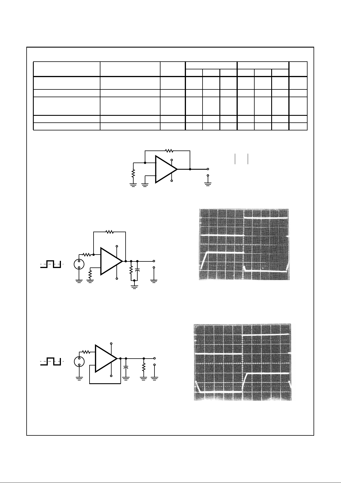
FIGURE 1. INPUT OFFSET VOLTAGE TEST CIRCUIT
FIGURE 2A. TEST CIRCUIT FIGURE 2B. RESPONSE TO 1kHz, 20V
P-P
SQUARE WAVE
FIGURE 2. INVERTING AMPLIFIER
FIGURE 3A. TEST CIRCUIT
FIGURE 3B. RESPONSE TO 20V
P-P
, 1kHz SQUARE WAVE INPUT
+
-
10K
V+
+15V
V
OUT
7
6
3
2
4
-15V
V-
100Ω
V
IO
V
OUT
100
---------------
=
10K
+15V
V
OUT
7
6
3
2
4
-15V
R
L
10K
200pF
5K
+10V
+10V
0V
1kHz
10K
V
OUT
= -V
IN
+
-
V
IN
0
0
Top Trace: Input Voltage, Bottom Trace: Output Voltage
Vertical Scale: 10V/Div., Horizontal Scale: 0.1ms/Div.
-
+
+15V
V
OUT
7
6
2
3
4
-15V
2K
200pF
+10V
+10V
0V
10K
SIMULATED
V
IN
LOAD
Top Trace: Input Voltage; Bottom Trace: Output Voltage
Vertical Scale: 10V/Div.; Horizontal Scale: 0.1ms/Div.
0
0
CA3193, CA3193A

4
Functional Block Diagram
FIGURE 3. VOLTAGE FOLLOWER
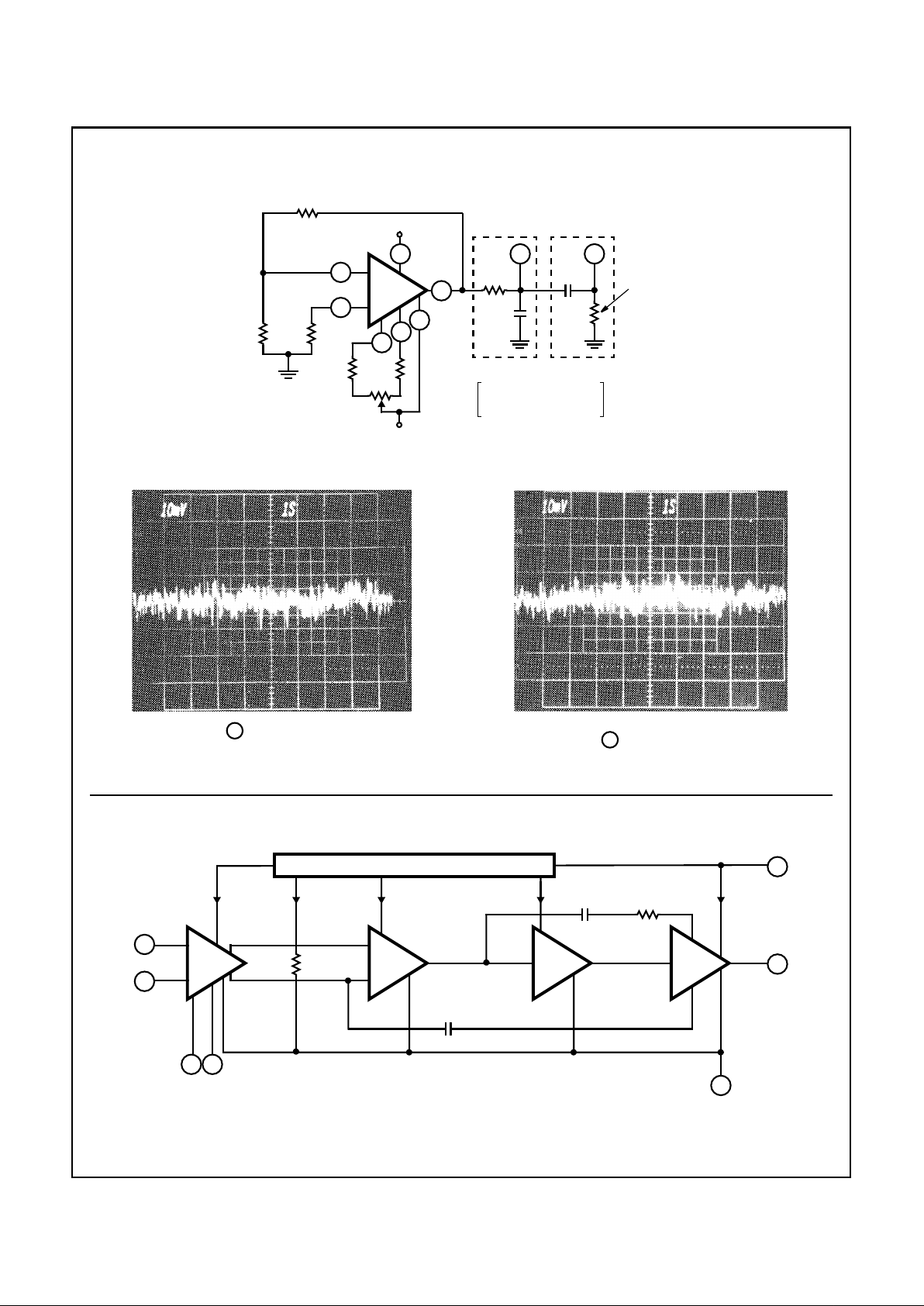
FIGURE 4A. TEST CIRCUIT - 0.1Hz TO 10Hz
FIGURE 4B. OUTPUT WAVEFORM - 0Hz TO 10Hz NOISE
FIGURE 4C. OUTPUT WAVEFORM - 0.1Hz TO 10Hz NOISE
FIGURE 4. LOW FREQUENCY NOISE
Test Circuits and Waveforms
(Continued)
+15V
-15V
2.2MΩ
2
3
1
5
4
7
1%
B
6
A
3.3kΩ
1%
4.7µF
1%
1MΩ
2.2µF
1%
100Ω1%100Ω
1%
20kΩ 20kΩ
1kΩ
CA3193
LOW PASS
FILTER
DC TO 10Hz
HIGH PASS
FILTER
0.1 TO 10Hz
SCOPE
INPUT
RESISTANCE
V
NOISE
V
OUT
PP–
22x10
3
----------------------------=
A
B
A ≈ 2000
A
≈ 75 A ≈ 1
A ≈ 7
BIAS NETWORK
6
7
4
51
2
3
3µA
950µA
70µA
25K
+
-
INPUT
OFFSET
NULL
660µA 600µA
OUTPUT
V+
V-
2.3mA
7.5K20pF
6pF
CA3193, CA3193A
 Loading...