

Intersil Corporation CA3165 Datasheet
OBSOLETE PRODUCT
CA3165
May 1999
Call Central Applications 1-800-442-7747
or email: centapp@harris.com
Features
NO RECOMMENDED REPLACEMENT
• Switching Initiated by Damping of Internal Oscillator
• Proximity Sensing of Rotational Motion
[ /Title (CA3165)
• Repeatable Timing of Switching States
/Subject (Electronic Switching Circuit)
• Five Outputs - Two Complementary Pairs and One
/Author ()
Non-Inverting Output CA3165E1
/Keywords ()
• Two Outputs - One Complementary Pair CA3165E
/Creator ()
/DOCINFO pdfmark
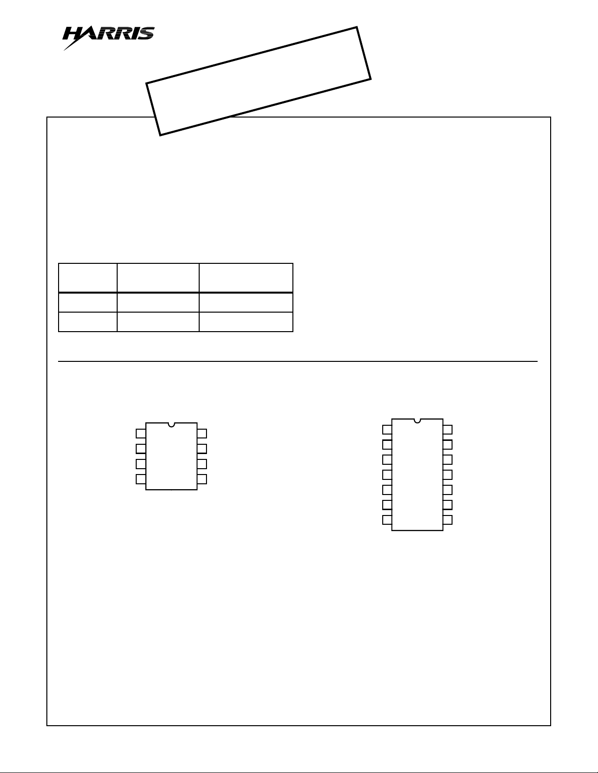
Part Number Information
PART
[ /PageMode /UseOutlines
NUMBER TEMPERATURE PACKAGE
/DOCVIEW pdfmark
CA3165E -40oC to +85oC 8 Lead Plastic DIP
CA3165E1 -40oC to +85oC 14 Lead Plastic DIP
Pinouts
Electronic Switching Circuit
Description
The CA3165 is a single chip electronic switching circuit
intended primarily for ignition applications. It includes an
oscillator that is amplitude-modulated by the rotor teeth of a
distributor, a detector that develops the positive going modulation envelope, a Schmitt trigger that eliminates switching
uncertainties. Both types include two complementary high
current switched outputs for driving power transistors requiring up to 120mA. The CA3165E also includes two complementary low current outputs that incorporate internal current
limiting and a non-inverting output amplifier with uncommitted input capable of switching 27mA.
The CA3165 is supplied in the 8 lead dual-in-line plastic
package (E suffix) and in the 14 lead dual-in-line plastic
package (E1 suffix).
OSC FB
SENSE
GND
OUTPUT
CA3165 (PDIP)
TOP VIEW
1
2
3
4
8
FB_RF
7
V+
6
DET_OUT
5
INV_OUT
OSC FB
SENSE
GND
OUTPUT
+SIGNAL
INV_OUT
–SIGNAL
CA3165 (PDIP)
TOP VIEW
1
2
3
4
5
6
7
14
NC
13
FB_R
V+
12
11
NC
10
DET_OUT
AMPL_IN
9
AMPL_OUT
8
F
CAUTION: These devices are sensitive to electrostatic discharge. Users should follow proper I.C. Handling Procedures.
Copyright
© Harris Corporation 1999
10-25
File Number 1278.3

Functional Block Diagrams
CA3165
DC SUPPLY 5V - 24V
NC
54
200Ω
100K
TO POWER
TRANSISTORS
AMP
976
847Ω
OUTPUT
8
6.8KΩ
0.0047µF
FEEDBACK
RESISTOR
(6kΩ ± 0.5%)
L = 100µH
≈ 53
Q
0.01µF
13
OSCILLATOR DET
1
2
220Ω
R
1500
pF
10
0.01
REPRESENTS
ROTOR LOADING
220Ω
3.5V - 18V
12
SCHMITT
TRIGGER
OUTPUT OUTPUT
SWITCHING
3
0.01µF
OSCILLATOR
CONDITION TERMINAL 10 TERMINAL 4 TERMINAL 5 TERMINAL 6 TERMINAL 7 TERMINAL 8
Unloaded Low High High Low Low Low
Loaded High Low Low High High High
FIGURE 1. FUNCTIONAL BLOCK DIAGRAM FOR CA3165E1
FEEDBACK
RESISTOR
(6.49kΩ)
L = 100µH
≈ 53
Q
0.1µF
8
OSCILLATOR DET
1
2
220Ω
R
†
R
A
B
1500
pF
OSCILLATOR
CONDITION TERMINAL 4 TERMINAL 5 TERMINAL 6
Unloaded High High Low
Loaded Low Low High
†
REPRESENTS
ROTOR LOADING
DC SUPPLY 5V - 24V
220Ω
7
SCHMITT
TRIGGER
6
0.01
†VALUES OF R
BY CORRELATION.
A
3.5V - 18V
OUTPUT
SWITCHING
3
AND RB DETERMINED
4
200Ω
5
TO POWER
TRANSISTORS
300Ω
INVERTED
OUTPUT
FIGURE 2. FUNCTIONAL BLOCK DIAGRAM FOR CA3165E
10-26
 Loading...