

Intersil Corporation CA3162, CA3162A Datasheet
CA3162, CA3162A
August 1997
Features
• Dual Slope A/D Conversion
• Multiplexed BCD Display
• Ultra Stable Internal Band Gap Voltage Reference
• Capable of Reading 99mV Below Ground with Single
Supply
• Differential Input
• Internal Timing - No External Clock Required
• Choice of Low Speed (4Hz) or High Speed (96Hz)
Conversion Rate
• “Hold” Inhibits Conversion but Maintains Delay
• Overrange Indication
- “EEE” for Reading Greater than +999mV, “-” for
Reading More Negative than -99mV When Used With
CA3161E
• Extended Temperature Range Version Available
Ordering Information
TEMP.
PART NUMBER
RANGE (oC) PACKAGE
A/D Converters for 3-Digit Display
Description
The CA3162E and CA3162AE are I2L monolithic A/D
converters that provide a 3 digit multiplexed BCD output.
They are used with the CA3161E BCD-to-Seven-Segment
Decoder/Driver and a minimum of external parts to implement a complete 3-digit display. The CA3162AE is identical
to the CA3162E except for an extended operating temperature range.
The CA3161E is described in the Display Drivers section of
this data book.
PKG.
NO.
CA3162E 0 to 70 16 Ld PDIP E16.3
CA3162AE -40 to 85 16 Ld PDIP E16.3
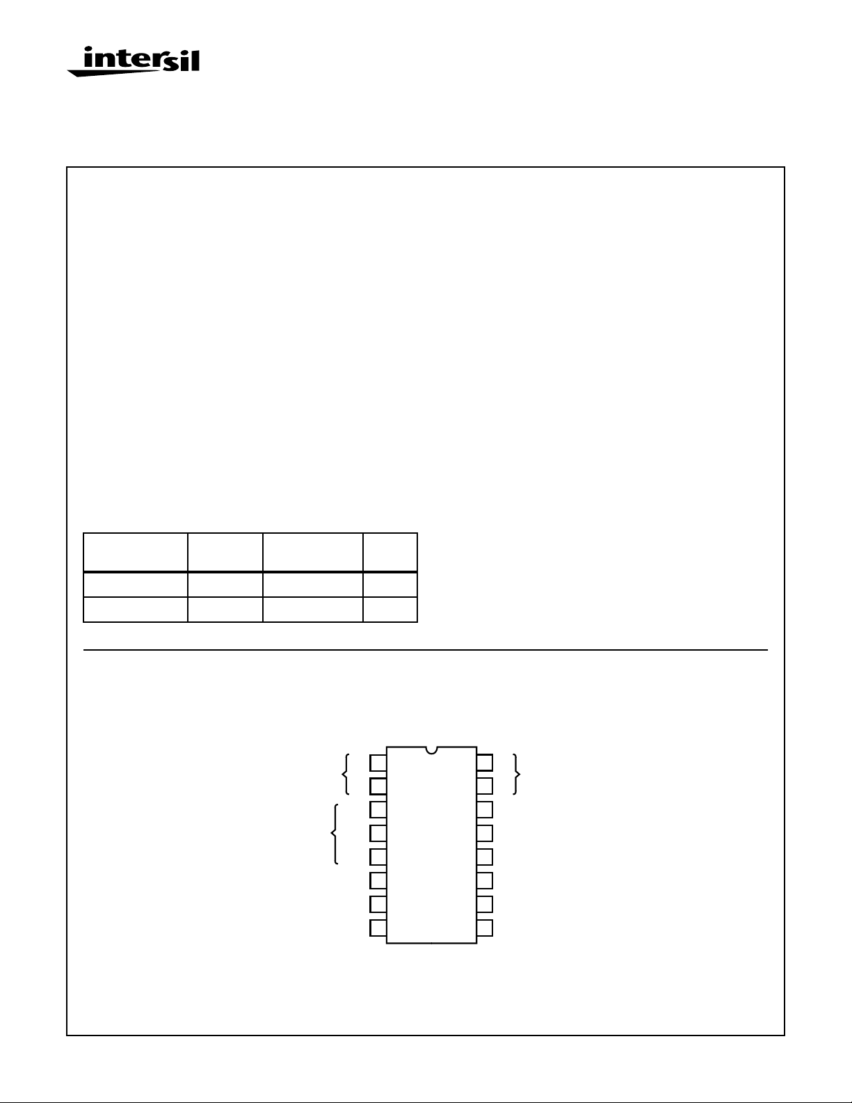
Pinout
1
1
2
BCD
OUTPUTS
DIGIT
SELECT
OUTPUTS
ZERO ADJ
NSD
MSD
LSD
HOLD/
BYPASS
GND
0
2
2
3
4
5
6
7
8
CA3162
(PDIP)
TOP VIEW
3
16
2
2
15
2
14
V+
13
GAIN ADJ
INTEGRATING
12
CAP
11
HIGH INPUT
10
LOW INPUT
9
ZERO ADJ
BCD
OUTPUTS
CAUTION: These devices are sensitive to electrostatic discharge; follow proper IC Handling Procedures.
1-888-INTERSIL or 321-724-7143 | Copyright © Intersil Corporation 1999
3-5
File Number 1080.2
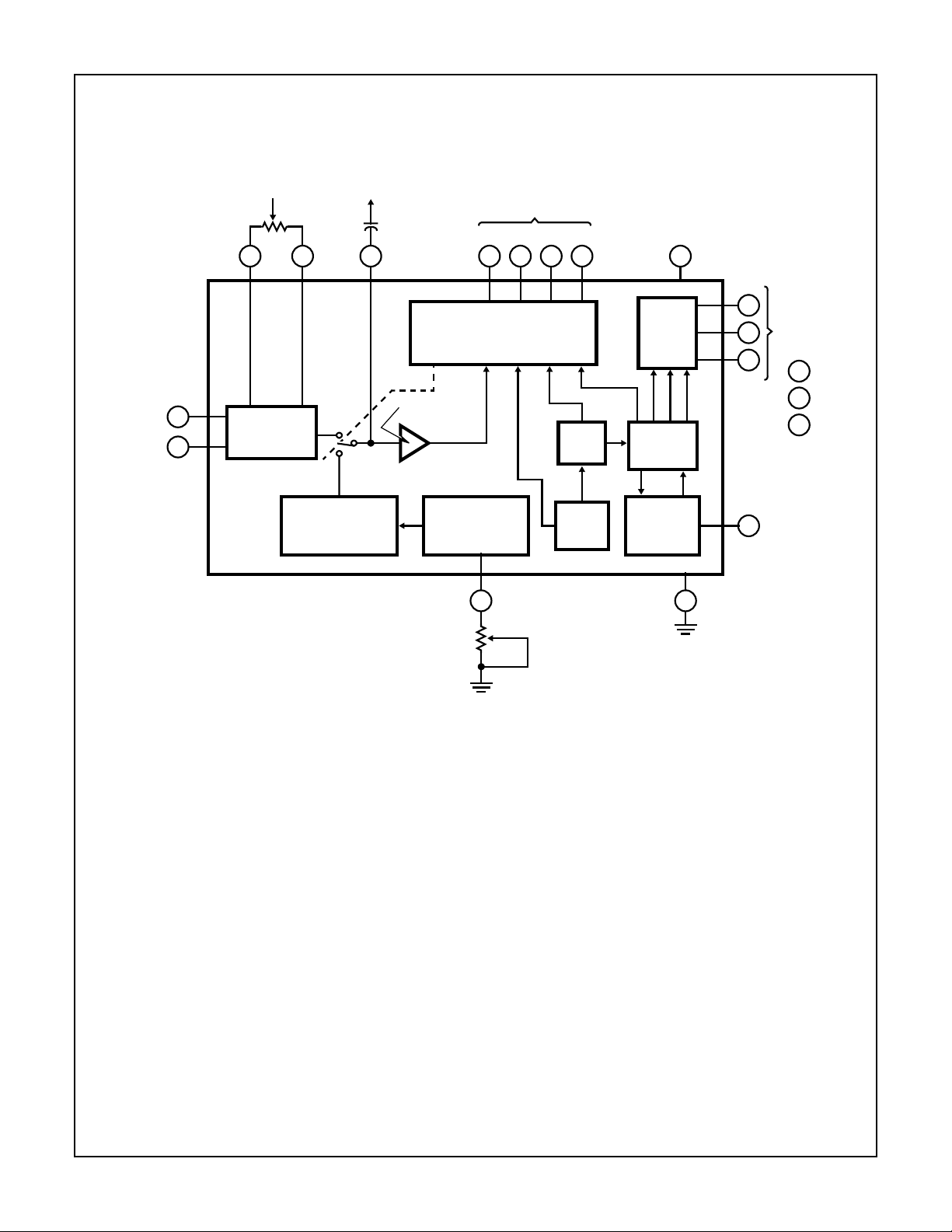
Functional Block Diagram
ZERO
ADJ
8 9 12 1 2 15 16 14
HIGH INPUT
LOW INPUT
11
10
V/I
CONVERTER
CA3162, CA3162A
V+V+
INTEGRATING
CAP
CONTROL LOGIC
COUNTERS AND MULTIPLEX
THRESHOLD
DET.
BCD OUTPUTS
1202223
2
÷2048
DIGIT
DRIVE
÷96
V+
3
4
5
DIGIT SELECT
OUTPUTS †
4
= MSD
5
= LSD
3
= NSD
†
MSD = MOST SIGNIFICANT DIGIT
NSD = NEXT SIGNIFICANT DIGIT
LSD = LEAST SIGNIFICANT DIGIT
REFERENCE
CURRENT
GENERATOR
BAND GAP
REFERENCE
GAIN
ADJ
OSC
HOLD/
BYPASS
GATES
CONVERSION
6
CONTROL
GND
713
3-6

CA3162, CA3162A
Absolute Maximum Ratings Thermal Information
DC Supply Voltage (Between Pins 7 and 14). . . . . . . . . . . . . . . +7V
Input Voltage (Pin 10 or 11 to Ground). . . . . . . . . . . . . . . . . . . ±15V
Operating Conditions
Temperature Range
CA3162E. . . . . . . . . . . . . . . . . . . . . . . . . . . . . . . . . . . . .0 to 75oC
CA3162AE . . . . . . . . . . . . . . . . . . . . . . . . . . . . . . . -40oC to 85oC
CAUTION: Stresses above those listed in “Absolute Maximum Ratings” may cause permanent damage to the device. This is a stress only rating and operation
of the device at these or any other conditions above those indicated in the operational sections of this specification is not implied.
NOTE:
1. θJA is measured with the component mounted on an evaluation PC board in free air.
Thermal Resistance (Typical, Note 1) θJA (oC/W)
PDIP Package. . . . . . . . . . . . . . . . . . . . . . . . . . . . . 90
Maximum Junction Temperature. . . . . . . . . . . . . . . . . . . . . . . 150oC
Maximum Storage Temperature Range . . . . . . . . . .-65oC to 150oC
Maximum Lead Temperature (Soldering 10s). . . . . . . . . . . . . 300oC
Electrical Specifications T
PARAMETER TEST CONDITIONS MIN TYP MAX UNITS
Operating Supply Voltage Range, V+ 4.5 5 5.5 V
Supply Current, I+ 100kΩ to V+ on Pins 3, 4, 5 - - 17 mA
Input Impedance, Z
Input Bias Current, I
Unadjusted Zero Offset V11-V10 = 0V, Read Decoded Output -12 - +12 mV
Unadjusted Gain V11-V10 = 900mV, Read Decoded Output 846 - 954 mV
Linearity Notes 1 and 2 -1 - +1 Count
Conversion Rate
Slow Mode Pin 6 = Open or GND - 4 - Hz
Fast Mode Pin 6 = 5V - 96 - Hz
Conversion Control Voltage (Hold Mode)
at Pin 6
Common Mode Input Voltage Range, V
BCD Sink Current at Pins 1, 2, 15, 16 V
I
IB
= 25oC, V+ = 5V, Zero Pot Centered, Gain Pot = 2.4kΩ, Unless Otherwise Specified
A
- 100 - MΩ
Pins 10 and 11 - -80 - nA
0.8 1.2 1.6 V
ICR
Notes 3, 4 -0.2 - +0.2 V
≥ 0.5V, at Logic Zero State 0.4 1.6 - mA
BCD
Digit Select Sink Current at Pins 3, 4, 5 V
Zero Temperature Coefficient VI = 0V, Zero Pot Centered - 10 - µV/oV
Gain Temperature Coefficient VI = 900mV, Gain Pot = 2.4kΩ - 0.005 - %/oC
NOTES:
1. Apply 0V across V11 to V10. Adjust zero potentiometer to give 000mV reading. Apply 900mV to input and adjust gain potentiometer to
give 900mV reading.
2. Linearity is measured as a difference from a straight line drawn through zero and positive full scale. Limits do not include ±0.5 count bit
digitizing error.
3. For applications where low input pin 10 is not operated at pin 7 potential, a return path of not more than 100kΩ resistance must be provided
for input bias currents.
4. The common mode input voltage above ground cannot exceed +0.2V if the full input signal range of 999mV is required at pin 11. That is,
pin 11 may not operate higher than 1.2V positive with respect to ground or 0.2V negative with respect to ground. If the maximum input
signal is less than 999mV, the common mode input voltage may be raised accordingly.
Select = 4V at Logic Zero State 1.6 2.5 - mA
DIGIT
3-7
 Loading...