

Intersil Corporation CA3140T, CA3140M96, CA3140M, CA3140E, CA3140AT Datasheet
...
CA3140, CA3140A
Data Sheet September 1998 File Number 957.4
4.5MHz, BiMOS Operational Amplifier with
MOSFET Input/Bipolar Output
The CA3140A and CA3140 are integrated circuit operational
amplifiers that combine the advantages of high voltage PMOS
transistors with high voltage bipolar transistors on a single
monolithic chip.
The CA3140A and CA3140 BiMOS operational amplifiers
feature gate protected MOSFET (PMOS) transistors in the
input circuit to provide very high input impedance, very low
input current, and high speed performance. The CA3140A
and CA3140 operateat supply voltage from 4V to 36V (either
single or dual supply). These operational amplifiers are
internally phase compensated to achieve stable operation in
unity gain follower operation, and additionally, have access
terminal for a supplementary external capacitor if additional
frequency roll-off is desired. Terminals are also provided for
use in applications requiring input offset voltage nulling. The
use of PMOS field effect transistors in the input stage results
in common mode input voltage capability down to 0.5V below
the negative supply terminal, an important attribute for single
supply applications. The output stage uses bipolar transistors
and includes built-in protection against damage from load
terminal short circuiting to either supply rail or to ground.
The CA3140 Series has the same 8-lead pinout used for the
“741” and other industry standard op amps. The CA3140A and
CA3140 are intended for operation atsupply voltages up to 36V
(±18V).
Ordering Information
PART NUMBER
(BRAND)
CA3140AE -55 to 125 8 Ld PDIP E8.3
CA3140AM
(3140A)
CA3140AS -55 to 125 8 Pin Metal Can T8.C
CA3140AT -55 to 125 8 Pin Metal Can T8.C
CA3140E -55 to 125 8 Ld PDIP E8.3
CA3140M
(3140)
CA3140M96
(3140)
CA3140T -55 to 125 8 Pin Metal Can T8.C
TEMP.
RANGE (oC) PACKAGE
-55 to 125 8 Ld SOIC M8.15
-55 to 125 8 Ld SOIC M8.15
-55 to 125 8 Ld SOIC Tape
and Reel
PKG.
NO.
Features
• MOSFET Input Stage
- Very High Input Impedance (Z
- Very Low Input Current (I
- Wide Common Mode InputV oltageRange (V
) -1.5TΩ (Typ)
IN
) -10pA (Typ) at ±15V
l
lCR
)- Can be
Swung 0.5V Below Negative Supply Voltage Rail
- Output Swing Complements Input Common Mode
Range
• Directly Replaces Industry Type 741 in Most
Applications
Applications
• Ground-Referenced Single Supply Amplifiers in Automobile and Portable Instrumentation
• Sample and Hold Amplifiers
• Long Duration Timers/Multivibrators
(µseconds-Minutes-Hours)
• Photocurrent Instrumentation
• Peak Detectors
• Active Filters
• Comparators
• Interface in 5V TTL Systems and Other Low
Supply Voltage Systems
• All Standard Operational Amplifier Applications
• Function Generators
• Tone Controls
• Power Supplies
• Portable Instruments
• Intrusion Alarm Systems
Pinouts
CA3140 (METAL CAN)
TOP VIEW
OFFSET
NULL
INV.
INPUT
NON-INV.
INPUT
OFFSET
NULL
INV. INPUT
NON-INV.
INPUT
TAB
1
-
2
+
3
CA3140 (PDIP, SOIC)
TOP VIEW
1
2
3
4
V-
STROBE
8
V+
7
6
OFFSET
5
4
V- AND CASE
NULL
-
+
OUTPUT
8
STROBE
7
V+
6
OUTPUT
OFFSET
5
NULL
1
CAUTION: These devices are sensitive to electrostatic discharge; follow proper IC Handling Procedures.
1-888-INTERSIL or 321-724-7143
| Copyright © Intersil Corporation 1999

CA3140, CA3140A
Absolute Maximum Ratings Thermal Information
DC Supply Voltage (Between V+ and V- Terminals) . . . . . . . . . 36V
Differential Mode Input Voltage . . . . . . . . . . . . . . . . . . . . . . . . . . 8V
DC Input Voltage . . . . . . . . . . . . . . . . . . . . . . (V+ +8V) To (V- -0.5V)
Input Terminal Current. . . . . . . . . . . . . . . . . . . . . . . . . . . . . . . . 1mA
Output Short Circuit Duration (Note 2). . . . . . . . . . . . . . . . Indefinite
Operating Conditions
Temperature Range . . . . . . . . . . . . . . . . . . . . . . . . . -55oC to 125oC
CAUTION: Stresses above those listed in “Absolute Maximum Ratings” may cause permanent damage to the device. This is a stress only rating and operation of the
device at these or any other conditions above those indicated in the operational sections of this specification is not implied.
NOTES:
1. θJA is measured with the component mounted on an evaluation PC board in free air.
2. Short circuit may be applied to ground or to either supply.
Thermal Resistance (Typical, Note 1) θJA (oC/W) θJC (oC/W)
PDIP Package . . . . . . . . . . . . . . . . . . . 100 N/A
SOIC Package . . . . . . . . . . . . . . . . . . . 160 N/A
Metal Can Package . . . . . . . . . . . . . . . 170 85
Maximum Junction Temperature (Metal Can Package). . . . . . . 175oC
Maximum Junction Temperature (Plastic Package) . . . . . . . 150oC
Maximum Storage Temperature Range. . . . . . . . . . -65oC to 150oC
Maximum Lead Temperature (Soldering 10s) . . . . . . . . . . . . 300oC
(SOIC - Lead Tips Only)
Electrical Specifications V
= ±15V, TA = 25oC
SUPPLY
TYPICAL VALUES
PARAMETER SYMBOL TEST CONDITIONS
Input Offset Voltage Adjustment Resistor Typical Value of Resistor
4.7 18 kΩ
UNITSCA3140 CA3140A
Between Terminals 4 and 5 or 4 and 1 to
Input Resistance R
Input Capacitance C
Output Resistance R
Equivalent Wideband Input Noise Voltage
Adjust Max V
I
I
O
e
BW = 140kHz, RS = 1MΩ 48 48 µV
N
IO
1.5 1.5 TΩ
44pF
60 60 Ω
(See Figure 27)
Equivalent Input Noise Voltage (See Figure 35) e
RS = 100Ω f = 1kHz 40 40 nV/√Hz
N
f = 10kHz 12 12 nV/√Hz
Short Circuit Current to Opposite Supply IOM+ Source 40 40 mA
IOM- Sink 18 18 mA
Gain-Bandwidth Product, (See Figures 6, 30) f
T
4.5 4.5 MHz
Slew Rate, (See Figure 31) SR 9 9 V/µs
Sink Current From Terminal 8 To Terminal 4 to
220 220 µA
Swing Output Low
Transient Response (See Figure 28) t
Settling Time at 10V
, (See Figure 5) t
P-P
OS Overshoot 10 10 %
S
r
RL = 2kΩ
CL = 100pF
RL = 2kΩ
CL = 100pF
Voltage Follower
Rise Time 0.08 0.08 µs
To 1mV 4.5 4.5 µs
To 10mV
1.4 1.4 µs
Electrical Specifications For Equipment Design, at V
= ±15V, TA = 25oC, Unless Otherwise Specified
SUPPLY
CA3140 CA3140A
PARAMETER SYMBOL
Input Offset Voltage |V
|- 5 15- 2 5mV
IO
UNITSMIN TYP MAX MIN TYP MAX
Input Offset Current |IIO| - 0.5 30 - 0.5 20 pA
Input Current I
Large Signal Voltage Gain (Note 3)
(See Figures 6, 29)
I
A
OL
- 10 50 - 10 40 pA
20 100 - 20 100 - kV/V
86 100 - 86 100 - dB
2

CA3140, CA3140A
Electrical Specifications For Equipment Design, at V
= ±15V, TA = 25oC, Unless Otherwise Specified (Continued)
SUPPLY
CA3140 CA3140A
PARAMETER SYMBOL
Common Mode Rejection Ratio
CMRR - 32 320 - 32 320 µV/V
(See Figure 34)
Common Mode Input Voltage Range (See Figure 8) V
Power-Supply Rejection Ratio,
PSRR - 100 150 - 100 150 µV/V
∆VIO/∆VS (See Figure 36)
Max Output Voltage (Note 4)
(See Figures 2, 8)
70 90 - 70 90 - dB
ICR
-15 -15.5 to +12.5 11 -15 -15.5 to +12.5 12 V
76 80 - 76 80 - dB
VOM+ +12 13 - +12 13 - V
VOM- -14 -14.4 - -14 -14.4 - V
UNITSMIN TYP MAX MIN TYP MAX
Supply Current (See Figure 32) I+ - 4 6 - 4 6 mA
Device Dissipation P
D
- 120 180 - 120 180 mW
Input Offset Voltage Temperature Drift ∆VIO/∆T- 8 - - 6 -µV/oC
NOTES:
3. At VO = 26V
, +12V, -14V and RL = 2kΩ.
P-P
4. At RL = 2kΩ.
Electrical Specifications For Design Guidance At V+ = 5V, V- = 0V, T
= 25oC
A
TYPICAL VALUES
PARAMETER SYMBOL
UNITSCA3140 CA3140A
Input Offset Voltage |VIO|5 2mV
Input Offset Current |IIO| 0.1 0.1 pA
Input Current I
Input Resistance R
Large Signal Voltage Gain (See Figures 6, 29) A
I
I
OL
22pA
11TΩ
100 100 kV/V
100 100 dB
Common Mode Rejection Ratio CMRR 32 32 µV/V
90 90 dB
Common Mode Input Voltage Range (See Figure 8) V
ICR
-0.5 -0.5 V
2.6 2.6 V
Power Supply Rejection Ratio PSRR
∆VIO/∆V
S
100 100 µV/V
80 80 dB
Maximum Output Voltage (See Figures 2, 8) VOM+3 3 V
VOM- 0.13 0.13 V
Maximum Output Current: Source IOM+10 10mA
Sink
I
-1 1mA
OM
Slew Rate (See Figure 31) SR 7 7 V/µs
Gain-Bandwidth Product (See Figure 30) f
T
3.7 3.7 MHz
Supply Current (See Figure 32) I+ 1.6 1.6 mA
Device Dissipation P
D
88mW
Sink Current from Terminal 8 to Terminal 4 to Swing Output Low 200 200 µA
3

Block Diagram
CA3140, CA3140A
Schematic Diagram
D
1
Q
1
Q
7
2mA 4mA
BIAS CIRCUIT
CURRENT SOURCES
AND REGULATOR
+
200µA 200µA1.6mA 2µA 2mA
V+
7
3
≈
INPUT
-
2
A ≈ 10
5
1 8
A
10,000
C
12pF
A ≈ 1
1
OUTPUT
6
V-
4
STROBE
OFFSET
NULL
DYNAMIC CURRENT SINKOUTPUT STAGESECOND STAGEINPUT STAGEBIAS CIRCUIT
7
V+
D
7
Q
Q
2
Q
6
Q
5
3
Q
4
R
9
50Ω
R
10
1K
Q
R
19
11
20Ω
Q
R
12K
R
13
5K
20
D
8
R
14
20K
12
R
1
8K
INVERTING
INPUT
NON-INVERTING
INPUT
Q
8
D
2
2
-
+
3
R
500Ω
Q
R
500Ω
5 1 8
NOTE: All resistance values are in ohms.
Q
Q
17
R
8
1K
Q
18
D
3
2
11
4
D
4
D
5
Q
Q
10
9
C
12pF
Q
1
Q
14
13
R
6
50Ω
Q
15
R
500Ω
R
3
500Ω
Q
12
5
21
6
OUTPUT
Q
16
D
6
R
7
30Ω
4
STROBEOFFSET NULL
V-
4

CA3140, CA3140A
Application Information
Circuit Description
As shown in the block diagram, the input terminals may be
operated down to 0.5V below the negative supply rail. Two
class A amplifier stages provide the voltage gain, and a
unique class AB amplifier stage provides the current gain
necessary to drive low-impedance loads.
A biasing circuit providescontrol of cascoded constant current
flow circuits in the first and second stages. The CA3140
includes an on chip phase compensating capacitor that is
sufficient for the unity gain voltage follower configuration.
Input Stage
The schematic diagram consists of a differential input stage
using PMOS field-effect transistors (Q
mirror pair of bipolar transistors (Q
resistors together with resistors R
transistors also function as a differential-to-single-ended
converter to provide base current drive to the second stage
bipolar transistor (Q
). Offset nulling, when desired, can be
13
effected with a 10kΩ potentiometer connected across
Terminals 1 and 5 and withits slider arm connected to Terminal
4. Cascode-connected bipolar transistors Q
constant current source for the input stage. The base biasing
circuit for the constant current source is described
subsequently. The small diodes D
protection against high voltage transients, e.g., static electricity.
Second Stage
Most of the voltage gain in the CA3140 is provided by the
second amplifier stage, consisting of bipolar transistor Q
and its cascode connected load resistance provided by
bipolar transistors Q
, Q4. On-chip phase compensation,
3
sufficient fora majority of the applications is provided by C
Additional Miller-Effect compensation (roll off) can be
accomplished, when desired, by simply connecting a small
capacitor between Terminals 1 and 8. Terminal 8 is also
used to strobe the output stage into quiescence. When
terminal 8 is tied to the negative supply rail (Terminal 4) by
mechanical or electrical means, the output Terminal 6
swings low, i.e., approximately to Terminal 4 potential.
Output Stage
The CA3140 Series circuits employ a broad band output stage
that can sink loads to the negative supply to complement the
capability of the PMOS input stage when operating near the
negative rail. Quiescent current in the emitter-follo wer cascade
circuit (Q
whose base currents are “mirrored” to current flowing through
diode D
operating such that output Terminal 6 is sourcing current,
transistor Q
from the V+bus (T erminal7), via D
conditions, the collector potential of Q
permit the necessary flow of base current to emitter follower
Q
17
, Q18) is established by transistors (Q14, Q15)
17
in the bias circuit section. When the CA3140 is
2
functions as an emitter-followertosource current
18
which, in turn, drives Q18.
, Q10) working into a
9
, Q12) functioning as load
11
through R5. The mirror pair
2
, Q5 are the
2
, D4, D5 provide gate oxide
3
, and R11. Under these
7,R9
is sufficiently high to
13
13
1
When the CA3140 is operating such that output Terminal 6 is
sinking current to the V - b us , transistor Q16 is the current
sinking element. Transistor Q
with current fed by wayof Q
turn, is biased by current flow through R
is mirror connected to D6, R7,
16
, and Q20. T r ansistorQ20,in
21,R12
, zener D8, and R14.
13
The dynamic current sink is controlled byvoltage level sensing.
Forpurposes of explanation, it is assumed that output Terminal
6 is quiescently established at the potential midpoint between
the V+ and V - supply rails . When output current sinking mode
operation is required, the collector potential of transistor Q
driven below its quiescent lev el, thereb y causing Q
17
13
, Q18 to
is
decrease the output voltage at Terminal 6. Thus, the gate
terminal of PMOStransistorQ
thereby reducing the channel resistance of Q
is displaced toward the V- bus,
21
21
. As a
consequence, there is an incremental increase in current flow
through Q
result, Q
the incremental change in output voltage caused by Q
, R12, Q21, D6, R7, and the base of Q16. As a
20
sinks current from Terminal 6 in direct response to
16
18
. This
sink current flows regardless of load; any excess current is
internally supplied by the emitter-follower Q
protection of the output circuit is provided by Q
. Short circuit
18
, which is
19
driven into conduction by the high voltage drop de v eloped
across R
conditions, the collector of Q
reduce the base current drive from Q
flow in Q
under output short circuit conditions. Under these
11
to the short circuited load terminal.
18
diverts current from Q4so as to
19
, thereby limiting current
17
Bias Circuit
Quiescent current in all stages (except the dynamic current
sink) of the CA3140 is dependent upon bias current flow in R
.
1
The function of the bias circuit is to establish and maintain
constant current flow through D
1,Q6,Q8
and D2.D1is a diode
connected transistor mirror connected in parallel with the base
.
emitter junctions of Q
current sampling diode that senses the emitter current of Q
, and Q3.D1maybeconsidered as a
1,Q2
6
and automatically adjusts the base current of Q6 (via Q1) to
maintain a constant current through Q
currents in Q
D
. Furthermore, current in diode connected transistor Q
1
are also determined by constant current flow
2,Q3
, Q8, D2. The base
6
2
establishes the currents in transistors Q14 and Q15.
Typical Applications
Wide dynamic range of input and output characteristics with
the most desirable high input impedance characteristics is
achievedin the CA3140 bythe use of an unique design based
upon the PMOS Bipolarprocess.Input common mode voltage
range and output swing capabilities are complementary,
allowing operation with the single supply down to 4V.
The wide dynamic range of these parameters also means
that this device is suitable for many single supply
applications, such as, for example,where one input is driven
below the potential of Terminal 4 and the phase sense of the
output signal must be maintained – a most important
consideration in comparator applications.
5
CA3140, CA3140A
Output Circuit Considerations
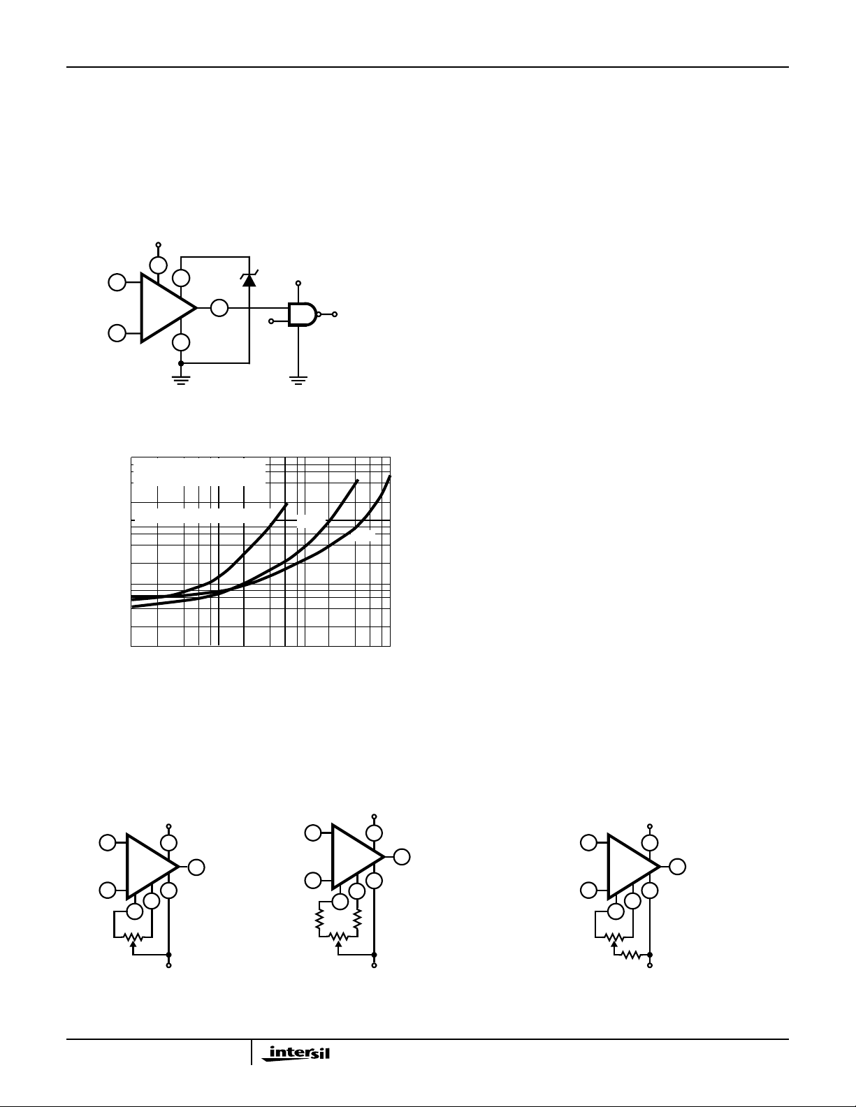
Excellent interfacing with TTL circuitry is easily achieved
with a single 6.2V zener diode connected to Terminal 8 as
shown in Figure 1. This connection assures that the
maximum output signal swing will not go more positive than
the zener voltage minus two base-to-emitter voltage drops
within the CA3140. These voltages are independent of the
operating supply voltage.
V+
5V TO 36V
7
8
2
CA3140
3
6.2V
6
4
FIGURE 1. ZENER CLAMPING DIODE CONNECTED TO
TERMINALS 8 AND 4 TO LIMIT CA3140 OUTPUT
SWING TO TTL LEVELS
)
1000
16
, Q
15
SATURATION VOLTAGE (mV)
OUTPUT STAGE TRANSISTOR (Q
SUPPLY VOLTAGE (V-) = 0V
TA = 25oC
SUPPLY VOLTAGE (V+) = +5V
100
10
1
0.01 0.1
LOAD (SINKING) CURRENT (mA)
FIGURE 2. VOLTAGE ACROSS OUTPUT TRANSISTORS (Q
AND Q16) vs LOAD CURRENT
Figure 2 shows output current sinking capabilities of the
CA3140 at various supply voltages. Output voltage swing to
the negative supply rail permits this device to operate both
power transistors and thyristors directly without the need for
LOGIC
SUPPLY
5V
≈5V
+15V
1.0 10
TYPICAL
TTL GATE
+30V
15
level shifting circuitry usually associated with the 741 series
of operational amplifiers.
Figure 4 shows some typical configurations. Note that a
series resistor, R
, is used in both cases to limit the drive
L
available to the driven device. Moreover, it is recommended
that a series diode and shunt diode be used at the thyristor
input to prevent large negative transient surges that can
appear at the gate of thyristors, from damaging the
integrated circuit.
Offset Voltage Nulling
The input offset voltage can be nulled by connecting a 10kΩ
potentiometer between Terminals 1 and 5 and returning its
wiper arm to terminal 4, see Figure 3A. This technique,
however, gives more adjustment range than required and
therefore, a considerable portion of the potentiometer
rotation is not fully utilized. Typical values of series resistors
(R) that may be placed at either end of the potentiometer,
see Figure 3B, to optimize its utilization range are given in
the Electrical Specifications table.
An alternate system is shown in Figure 3C. This circuit uses
only one additional resistor of approximately the value
shown in the table. For potentiometers, in which the
resistance does not drop to 0Ω at either end of rotation, a
value of resistance 10% lower than the values shown in the
table should be used.
Low Voltage Operation
Operation at total supply voltages as low as 4V is possible
with the CA3140. A current regulator based upon the PMOS
threshold voltage maintains reasonable constant operating
current and hence consistent performance down to these
lower voltages.
The low voltage limitation occurs when the upper extreme of
the input common mode voltage range extends do wn to the
voltage at Terminal 4. This limit is reached at a total supply
voltage just below 4V. The output voltage range also begins to
extend down to the negative supply r ail, b ut is slightly higher
than that of the input. Figure 8 shows these characteristics and
showsthat with 2Vdual supplies, the lowerextremeof the input
common mode voltage range is below ground potential.
V+
2
3
10kΩ
CA3140
5
1
7
4
V-
FIGURE 3A. BASIC
V+
2
6
3
R
10kΩ
FIGURE 3B. IMPROVED RESOLUTION
CA3140
5
1
7
6
4
R
V-
2
CA3140
3
1
10kΩ
FIGURE 3C. SIMPLER IMPROVED RESOLUTION
V+
7
6
4
5
R
V-
FIGURE 3. THREE OFFSET VOLTAGE NULLING METHODS
6
 Loading...