January 1999
Semiconductor
OBSOLETE PRODUCT
POSSIBLE SUBSTITUTE PRODUCT
HA-2525
CA3100
38MHz, Operational Amplifier
[ /Title
(CA31
00)
/Subject
(38MH
z,
Operational
Amplifier)
/Autho
r ()
/Keywords
(Harris
Semiconductor,
single,
operational
amplifier, op
amp,
general
purpose,
industrial
military
Features
• High Open Loop Gain at Video
Frequencies . . . . . . . . . . . . . . . . . . 42dB (Typ) at 1MHz
• Unity Gain
Crossover Frequency (f
• Full Power Bandwidth
V
= 18V
O
• Slew Rate
- 20dB Amplifier . . . . . . . . . . . . . . . . . . . . 70V/µs (Typ)
- Unity Gain Amplifier. . . . . . . . . . . . . . . . 25V/µs (Typ)
• Settling Time . . . . . . . . . . . . . . . . . . . . . . . . 0.6µs (Typ)
• Output Current. . . . . . . . . . . . . . . . . . . . . . ±15mA (Min)
• Single Capacitor Compensation
• Offset Null Terminals
. . . . . . . . . . . . . . . . . . . . . . . 1.2MHz (Typ)
P-P
) . . . . . . . . . . . . . 38MHz (Typ)
T
Applications
• Video Amplifiers
• Fast Peak Detectors
• Meter Driver Amplifiers
• High Frequency Feedback Amplifiers
• Video Pre-Drivers
• Oscillators
• Multivibrators
• Voltage Controlled Oscillator
• Fast Comparators
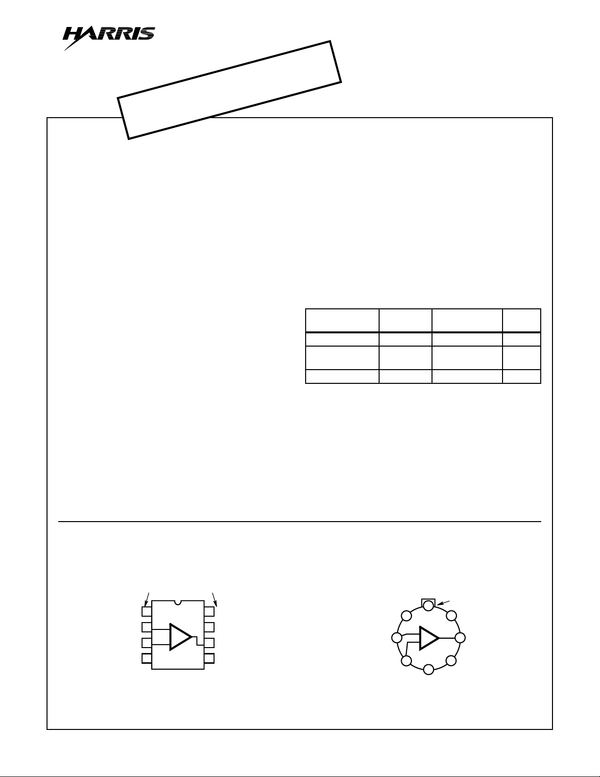
Pinouts
CA3100
(PDIP, SOIC)
TOP VIEW
PHASE COMPENSATION
OFFSET
NON-INV.
NULL
INV.
INPUT
INPUT
1
2
-
+
3
4
V-
8
7
6
5
V+
OUTPUT
OFFSET
NULL
Description
The CA3100 is a large signal wideband, high speed
operational amplifier which has a unity gain cross over
frequency (f
3dB corner frequency of approximately 110kHz. It can
operate at a total supply voltage of from 14V to 36V (±7V to
±18V when using split supplies) and can provide at least
18V
P-P
±15V supplies. The CA3100 can be compensated with a
single external capacitor and has DC offset adjust terminals
for those applications requiring offset null. (See Figure 1).
The CA3100 circuit contains both bipolar and PMOS transistors on a single monolithic chip.
) of approximately 38MHz and an open loop,
T
and 30mA
at the output when operating from
P-P
Part Number Information
PART NUMBER
(BRAND)
CA3100E -40 to 85 8 Ld PDIP E8.3
CA3100M
(3100)
CA3100T -55 to 125 8 Pin Metal Can T8.C
COMP AND
OFFSET NULL
TEMP.
RANGE (oC) PACKAGE
-40 to 85 8 Ld SOIC M8.15
CA3100
(METAL CAN)
TOP VIEW
PHASE
COMP
PHASE
INV.
INPUT
NON-INV.
INPUT
1
2
3
TAB
8
V+
7
-
+
4
V-
5
6
OFFSET
NULL
PKG.
NO.
OUTPUT
CAUTION: These devices are sensitive to electrostatic discharge. Users should follow proper IC Handling Procedures.
© Harris Corporation 1999
Copyright
3-1
File Number 625.4

CA3100
Absolute Maximum Ratings Thermal Information
Supply Voltage (Between V+ and V- Terminals). . . . . . . . . . . . . 36V
Differential Input Voltage. . . . . . . . . . . . . . . . . . . . . . . . . . . . . . . 12V
Input Voltage to Ground . . . . . . . . . . . . . . . . . . . . . . . . . . . . V+ to V-
Offset Terminal to V- Terminal Voltage . . . . . . . . . . . . . . . . . . ±0.5V
Output Current (Note 2) . . . . . . . . . . . . . . . . . . . . . . . . . . . . . .50mA
Operating Conditions
Temperature Range
CA3100E, CA3100M. . . . . . . . . . . . . . . . . . . . . . . -40oC to 85oC
CA3100T. . . . . . . . . . . . . . . . . . . . . . . . . . . . . . . -55oC to 125oC
CAUTION: Stresses above those listed in “Absolute Maximum Ratings” may cause permanent damage to the device. This is a stress only rating and operation
of the device at these or any other conditions above those indicated in the operational sections of this specification is not implied.
NOTES:
1. θJA is measured with the component mounted on an evaluation PC board in free air.
2. CA3100 does not contain circuitry to protect against short circuits in the output.
Thermal Resistance (Typical, Note 1) θJA (oC/W) θJC (oC/W)
PDIP Package. . . . . . . . . . . . . . . . . . . 100 N/A
SOIC Package. . . . . . . . . . . . . . . . . . . 165 N/A
Metal Can Package. . . . . . . . . . . . . . . 170 85
Maximum Junction Temperature (Metal Can) . . . . . . . . . . . . . 175oC
Maximum Junction Temperature (Plastic Package) . . . . . . . 150oC
Maximum Storage Temperature Range . . . . . . . . . -65oC to 150oC
Maximum Lead Temperature (Soldering 10s). . . . . . . . . . . . 300oC
(SOIC - Lead Tips Only)
Electrical Specifications T
= 25oC, V
A
= ±15V, Unless Otherwise Specified
SUPPLY
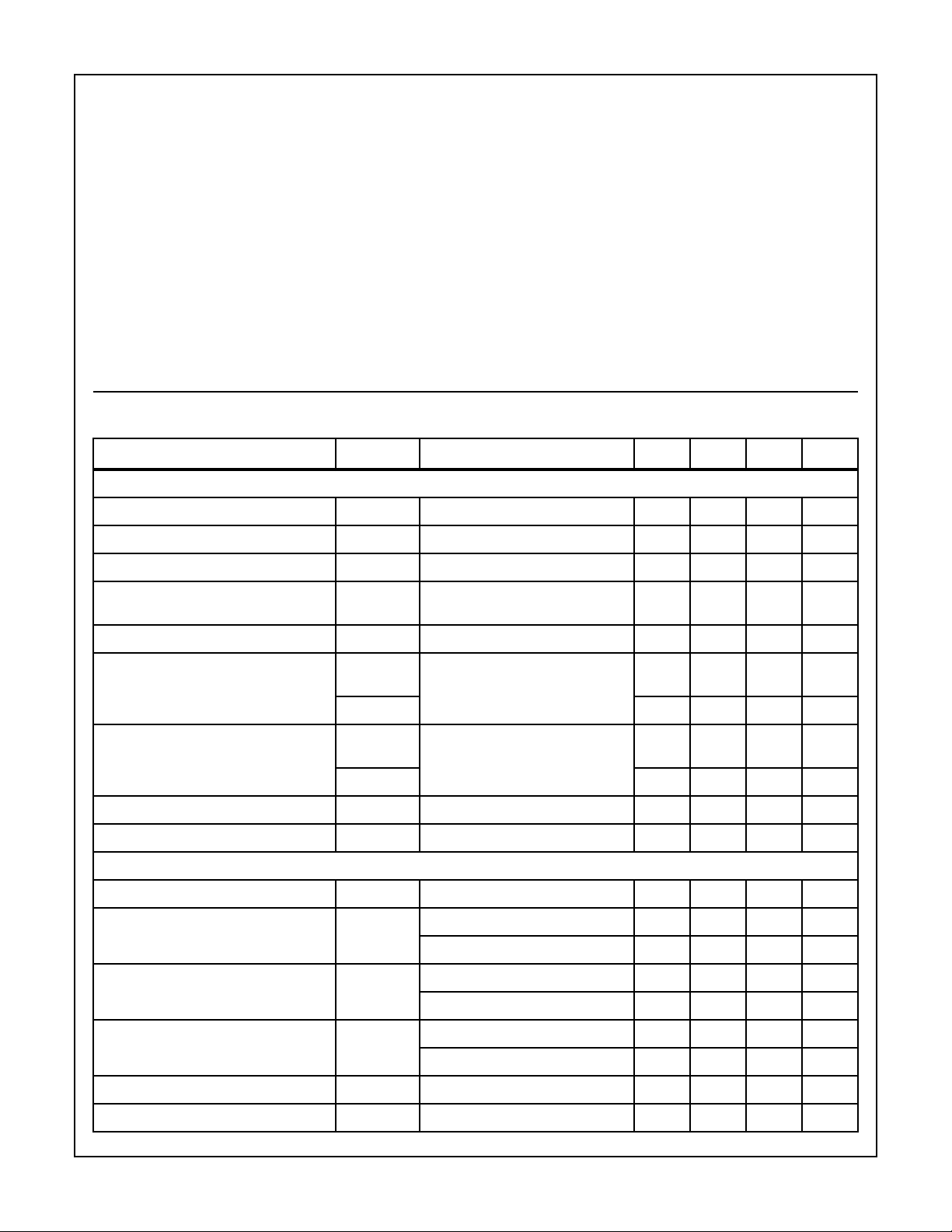
PARAMETER SYMBOL TEST CONDITIONS MIN TYP MAX UNITS
DC
Input Offset Voltage V
Input Bias Current I
Input Offset Current I
Common Mode Input Voltage Range V
IO
IB
IO
lCR
VO = 0 ±0.1V - ±1 ±5mV
VO = 0 ±1V - 0.7 2 µA
VO = 0 ±1V - ±0.05 ±0.4 µA
CMRR ≥ 76dB ±12 +14
-V
-13
Common Mode Rejection Ratio CMRR VCM = ±12V 76 90 - dB
Maximum Output Voltage VOM+ Differential Input Voltage = 0 ±0.1V,
+9 +11 - V
RL = 2kΩ
VOM- -9 -11 - V
Maximum Output Current IOM+ Differential Input Voltage = 0 + 0.1V,
+15 +30 - mA
RL = 250Ω
IOM- -15 -30 - mA
Supply Current I+ VO = 0 ±0.1V, RL≥ 10kΩ - 8.5 10.5 mA
Power Supply Rejection Ratio PSRR ∆V+ = ±1V, ∆V- = ±1V 60 70 - dB
DYNAMIC
Unity-Gain Crossover Frequency f
Open Loop Voltage Gain A
T
OL
CC = 0, VO = 0.3V
P-P
- 38 - MHz
f = 1kHz, VO = ±1V, (Note 3) 56 61 - dB
f = 1MHz, CC = 0, VO = 10V
P-P
36 42 - dB
Slew Rate SR AV = 10, CC = 0, VI = 1V (Pulse) 50 70 - V/µs
AV = 1, CC = 10pF, VI = 10V (Pulse) - 25 - V/µs
Full Power Bandwidth (Note 4) FPBW AV = 10, CC = 0, VO = 18V
AV = 1, CC = 10pF, VO = 18V
Open Loop Differential Input Impedance Z
Open Loop Output lmpedance Z
O
f = 1MHz - 30 - kΩ
I
f = 1MHz - 110 - Ω
P-P
P-P
0.8 1.2 - MHz
- 0.4 - MHz
3-2

CA3100
Electrical Specifications T
= 25oC, V
A
= ±15V, Unless Otherwise Specified (Continued)
SUPPLY
PARAMETER SYMBOL TEST CONDITIONS MIN TYP MAX UNITS
Wideband Noise Voltage (RTI) eN (Total) BW = 1MHz, RS = 1kΩ -8-µV
Settling Time (To Within ±50mV of 9V
Output Swing)
t
S
RL = 2kΩ, CL = 20pF - 0.6 - µs
NOTES:
3. Low frequency dynamic characteristic.
4. .
Full Power Bandwidth
Slew Rate
-------------------------- -=
πV
OP P–
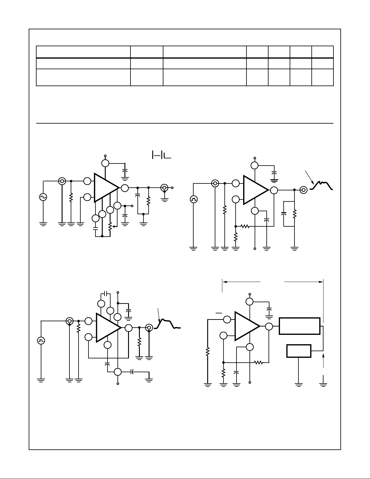
Test Circuits
V+
7
0.1µF
3
+
LEVEL
O
51Ω
V
I
HP606A
OR
EQUIV
SET V
TO GIVE
I
DESIRED V
AT TEST FREQUENCY
CA3100
-
2
1
8
C
C
NULL ADJUST
POTENTIOMETER
6
20pF
V-
4
5
0.1µF
R
X
10kΩ
AT FREQUENCY > 1MHz V
AND VOMEASURED WITH
HF8405A VECTOR
VOLTMETER
FIGURE 1. OPEN-LOOP VOLTAGE GAIN TEST CIRCUIT AND
OFFSET ADJUST CIRCUIT
V+
10pF
1
+10V
PULSE
t
≤ 10ns
R
t
WIDTH
≥ 1µs
V
I
3
51Ω
2
3
+
CA3100
-
5
500pF
0.1µF
7
6
2kΩ
0.1µF
4
AOL =
V
V
O
θ
V
I
2kΩ
WITH V
I
POTENTIOMETER (RX)
TO GIVE
= 0 ± 0.1V
V
O
SLOPE = SR
O
OL
V
O
= 0 ADJ
DC
I
V+
+1V
PULSE
t
≤ 10ns
R
t
WIDTH
≥ 1µs
7
+
CA3100
-
4
V-
0.1µF
0.1
µF
6
20
pF
V
I
3
2
51Ω
2kΩ
220Ω
SLOPE = SR
V
O
2kΩ
FIGURE 2. SLEW RATE IN 10X AMPLIFIER TEST CIRCUIT
AV = 100
+15V
INPUT REFERRED
NOISE VOLTAGE
e
NO
e
=
NI
100
3
2
R
S
47Ω
+
CA3100
-
0.1µF
7
4
0.1µF
420Ω
POST AMPL. AND
6
2 POLE 1MHz
FILTER
HP400EL
VTVM
RMS
e
NO
V-
FIGURE 3. FOLLOWER SLEW RATE TEST CIRCUIT
-15V
FIGURE 4. WIDEBAND INPUT NOISE VOLTAGE TEST CIRCUIT
3-3

CA3100
Test Circuits
9.1kΩ
±1V
(Continued)
+15V
3
+
CA3100
-
2
RL = 250Ω FOR IOM TEST
7
I
6
OM
=
V
250Ω
4
R
1kΩ
1kΩ
2kΩ
L
-15V
FIGURE 5. OUTPUT VOLTAGE SWING (VOM), OUTPUT
CURRENT SWING (I
) TEST CIRCUIT
OM
Schematic Diagram
R
12kΩ
NON-
INVERT
INPUT
3
R
4
6
750Ω
+
R
5
750Ω
1pF
2kΩ
O
V
= ±9V
I
V
OM
51Ω
2kΩ
1kΩ
2
3
-
CA3100
+
1
12pF
7
8
+15V
-15V
4
0.1µF
0.1
µF
VO = ±9V
6
20pF
2kΩ 2kΩ
SETTLING POINT TO SCOPE
FIGURE 6. SETTLING TIME TEST CIRCUIT
Q
Q
1
Q
5
Q
7
2
Q
6
Q
8
Q
R
2.5kΩ
3
1
7
V+
Q
4
INVERT
INPUT
2
R
10kΩ
Q
R
50Ω
V-
4
D
Q
Q
-
Q
11
Q
R
Q
20Ω
21
10
Q
22
7
23
Q
14
R
11
20Ω
12
15
Q
19
Q
20
9
D
4
Q
16
2
C
1
10pF
D
3
Q
R
200Ω
13
8
Q
10
Q
17
Q
D
5
R
9
200Ω
18
OUTPUT
6
8
PHASE
COMP
OFFSET
NULL
5
1
R
14
12
1.1kΩ
R
20Ω
13
R
1.1kΩ
R
15
150Ω
16
R
17
600Ω
R
19
600Ω
R
150Ω
18
OFFSET
NULL
AND PHASE
COMP
3-4

Typical Applications
+15V
INPUT
0.33µF
3kΩ
220Ω
3
+
CA3100
-
2
-15V
FIGURE 7. 20dB VIDEO AMPLIFIER FIGURE 8. 20dB VIDEO LINE DRIVER
7
4
2kΩ
3pF
CA3100
0.1µF
OUTPUT
6
0.1µF
-3dB BANDWIDTH≈ 20MHz
TOTAL INPUT NOISE
VOLTAGE REFERRED TO
INPUT
≈ 35µV
RMS
3dB BANDWIDTH = 15MHz
ACL = 20dB
INPUT
0.33µF
V
8V
5V
2V
1V
O
220Ω
GAIN = 20dB
3kΩ
DELIVERS FOLLOWING
PEAK VOLTAGES TO
50Ω LINE:
FREQ
1MHz
2MHz
4MHz
6MHz
+15V
6
2kΩ
0.1µF
4.7
kΩ
10Ω
10Ω
2N5320
OUTPUT TO
TERMINATED
50Ω TRANS-
MISSION LINE
2N5322
0.1µF
7
3
+
CA3100
-
2
1N5393
4
3pF
220Ω
-15V
+15V
0.1µF
6
1N914
0.1µF
VI(AC)
3kΩ
7
3
+
CA3100
-
2
4
1.2kΩ
-15V
FIGURE 9. FAST POSITIVE PEAK DETECTOR FIGURE 10. 1MHz METER-DRIVER AMPLIFIER
Typical Performance Curves
80
70
60
50
40
30
20
10
OPEN LOOP VOLTAGE GAIN (dB)
0
0.001 0.01 0.1 1 10 100
|AOL|
CC = 24pF
CC = 24pF
θ
0pF
12pF
FREQUENCY (MHz)
12pF
0pF
TA = 25oC
V
= ±15V
S
RL = 2kΩ
= 20pF
C
L
0pF
12pF
24pF
2N2102
V
(DC) =
O
+V
PEAK
I
1000pF
-270
-225
-180
-135
-90
-45
0
ZERO ADJ
200Ω
INPUT
IMPEDANCE
≈ 50kΩ
TEST
LEADS
70
60
50
40
30
20
10
OPEN LOOP VOLTAGE GAIN (dB)
OPEN LOOP PHASE SHIFT (DEGREES)
0
0.001 0.01 0.1 1 10 100
51kΩ
20kΩ
1
3
+
CA3100
-
2
-15V
FREQUENCY (MHz)
10pF
8
4
+15V
7
51kΩ
0.1
µF
250Ω POT.
25oC
125oC
0.1µF
6
330Ω
FULL SCALE
CALIBRATION
ADJUST
TA = -55oC
1V
FULL SCALE
1N914
+
-
VS = ±15V
= 2kΩ
R
L
CC = 0
RMS
1mA
FULL
SCALE
DC
METER
FIGURE 11. OPEN LOOP GAIN, OPEN LOOP PHASE SHIFT vs
FREQUENCY
FIGURE 12. OPEN LOOP GAIN vs FREQUENCY
3-5

CA3100
Typical Performance Curves
70
60
50
40
±12V
30
20
10
OPEN LOOP VOLTAGE GAIN (dB)
0
0.001 0.01 0.1 1 10 100
±10V
±7V
FREQUENCY (MHz)
(Continued)
TA = 25oC
R
C
C
VS = ±18V
= 2kΩ
L
= 20pF
L
= 0
C
25
20
15
10
COMP CAP PINS 1 TO 8 (pF)
5
0
0 6 (0) 10 (6) 20 (19.1)
±10V
NONINVERTING GAIN (dB), INVERTING GAIN (dB)
VS = ±15V
CLOSED LOOP GAIN (dB)
FIGURE 13. OPEN LOOP GAIN vs FREQUENCY FIGURE 14. REQUIRED COMPENSATION CAPACITANCE vs
CLOSED LOOP GAIN
350
TA = 25oC
VS = ±15V
300
+15V
+
CA3100
-
1
10
K
7
4
5
-15V
200
100
3
2
0 10203040
FREQUENCY (MHz)
80
60
40
SLEW RATE (V/µs)
20
0 5 10 15 20 25
VS = ±15V
±10V
COMP CAP PINS 1 TO 8 (pF)
TA = 25oC
= 2kΩ
R
L
= 20pF
C
L
OPEN LOOP OUTPUT IMPEDANCE (Ω)
6
V
O
TA = 25oC
R
= 2kΩ
L
C
= 20pF
L
HEWLETT
PACKARD
VECTOR
IMPEDANCE
METER4815A
FIGURE 15. SLEW RATE vs COMPENSATION CAPACITANCE FIGURE 16. TYPICAL OPEN LOOP OUTPUT IMPEDANCE vs
FREQUENCY
6
30
20
)
RMS
(µV
10
TOTAL INPUT REFERRED NOISE VOLTAGE
0
2
10
SOURCE RESISTANCE (Ω)
10
TA = 25oC
BW AT 6dB = 1MHz
3
FIGURE 17. WIDEBAND INPUT NOISE VOLTAGE vs SOURCE
RESISTANCE
4
10
10
5
10
4
10
IMPEDANCE (Ω)
OPEN LOOP DIFFERENTIAL INPUT
3
10
0.1 1 10 100
FREQUENCY (MHz)
TA = 25oC
VS = ±15V
FIGURE 18. TYPICAL OPEN LOOP DIFFERENTIAL INPUT
IMPEDANCE vs FREQUENCY
3-6

CA3100
Typical Performance Curves
25
20
)
P-P
15
10
OUTPUT VOLTAGE (V
5
0
0.01 0.1 1 10 100
CIRCUIT FIG. 3
(FOLLOWER)
FREQUENCY (MHz)
(Continued)
TA = 25oC
V
CIRCUIT FIG. 2
10X AMPL
S
FIGURE 19. MAXIMUM OUTPUT VOLTAGE SWING vs
FREQUENCY
15
12.5
10
VOM-
VOM+
= ±15V
TA = 25oC
TA = 25oC
15.0
12.5
10.0
+V
7.5
5.0
2.5
0
COMMON MODE INPUT VOLTAGE RANGE (V)
0 ±2.5 ±5 ±7.5 ±10 ±12.5 ±15 ±17.5 ±20
ICR
-V
ICR
SUPPLY VOLTAGE (V)
FIGURE 20. COMMON MODE INPUT VOLTAGE RANGE vs
SUPPLY VOLTAGE
TA = 25oC
15
12.5
10
7.5
5
2.5
MAXIMUM OUTPUT VOLTAGE (V)
0
0 ±2.5 ±5 ±7.5 ±10 ±12.5 ±15 ±17.5 ±20
SUPPLY VOLTAGE (V)
FIGURE 21. MAXIMUM OUTPUT VOLTAGE vs SUPPLY V OLTAGE
15.0
12.5
10.0
7.5
5.0
INPUT BIAS CURRENT (µA)
2.5
0
±2.5 ±5 ±7.5 ±10 ±12.5 ±15 ±17.5 ±20
0
SUPPLY VOLTAGE (V)
7.5
5
SUPPLY CURRENT (mA)
2.5
0
±2.5 ±5 ±7.5 ±10 ±12.5 ±15 ±17.5 ±20
0
SUPPLY VOLTAGE (V)
FIGURE 22. SUPPLY CURRENT vs SUPPLY VOLTAGE
TA = 25oC
FIGURE 23. INPUT BIAS CURRENT vs SUPPLY VOLTAGE
3-7
 Loading...