Intersil Corporation CA3098E Datasheet

T
C
U
D
O
TM
E
R
O
N
1
l
l
a
C
L
O
S
B
O
C
-
E
M
M
O
N
I
-
8
8
8
R
P
E
T
E
N
T
R
D
E
D
o
L
I
S
R
E
C
A
L
P
E
7
-
1
2
3
r
T
N
E
M
E
3
4
1
7
-
4
2
CA3098
January 1999 File Number 896.5
)
ma
itt
ith
,
ut
)
()
ds
duc
e,
tor,
t
ent,
Programmable Schmitt Trigger with
Memory, Dual Input Precision Level
Detector
The CA3098 Programmable Schm itt Trigge r is a monolithic
silicon integrated circuit desi gned to control high oper ating
current loads such as thyristors, lamps, relays, etc. The
CA3098 can be operated wit h eit her a single power supply
with maximum operating voltage of 16V, or a dual power
supply with maxi mu m operating voltage of ±8V. It can
directly control currents up to 150mA and operates with
microwatt st andby power dissipation when the current to be
controlled is less than 30mA. The CA3098 contains the
following major circuit function feat ures (see Block Diagram):
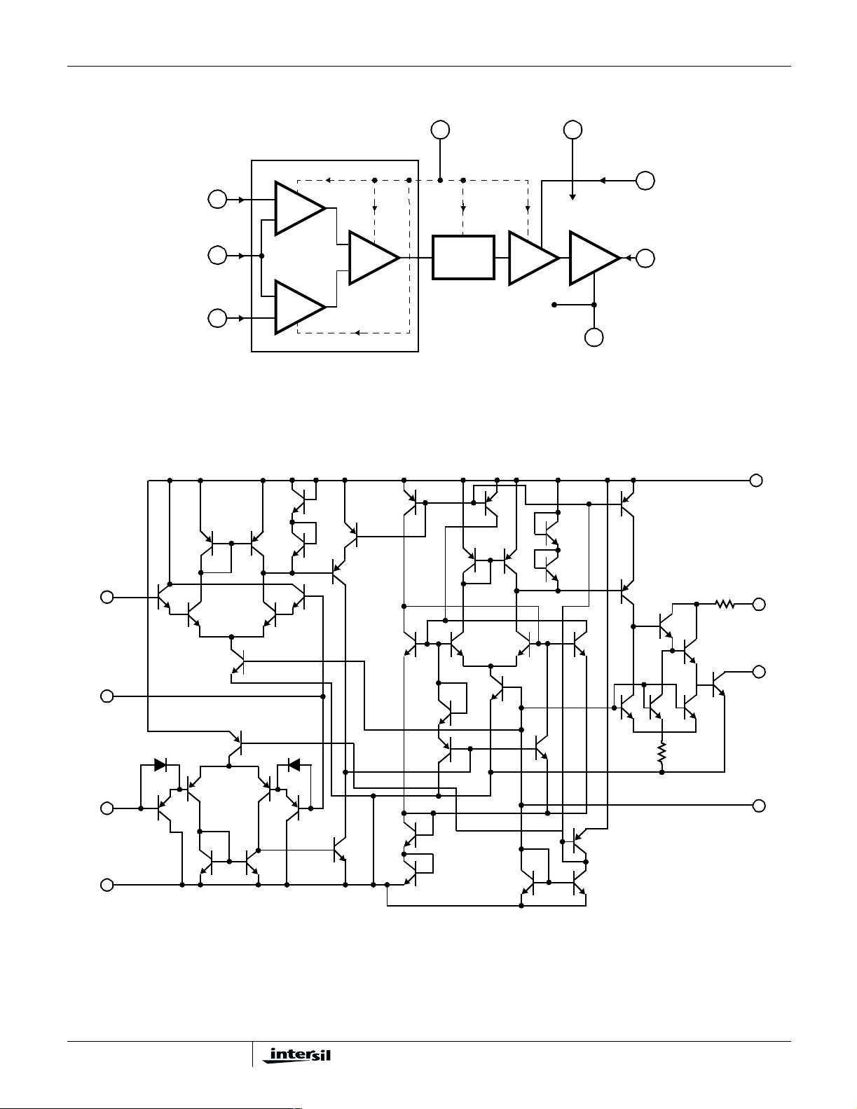
1. Differe nti al amplifiers and summer : the circuit uses two
differ ential amplifiers, one to compare the input voltage
with the “high” reference, and the other to compare the
input with the “ low” r eferenc e. The re sult ant output of the
differential amplifiers actuates a summer circuit which
delivers a trigger that initiat es a change in state of a flipflop.
2. Flip-flop: the flip-flop functions as a bistable “memory”
element that changes state in respon se to each trigger
command.
3. Driver and outpu t stag es: these stages per mit the circuit
to “sink” maximu m pea k load currents up to 150mA at
terminal 3.
4. Programmable operating current: the circuit incorporates
access at terminal 2 to permit programming the desired
quiescent operating current and performance parameters.
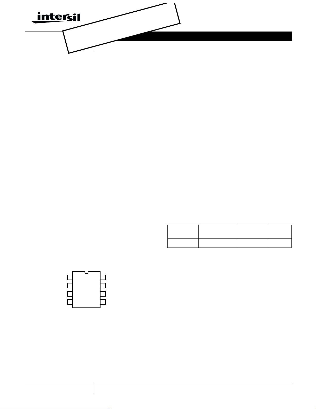
Pinout
CA3098
(PDIP)
TOP VIEW
Features
• Programmable Operati ng Current
• Micropower Standby Dissipation
• Direct Control of Currents Up to. . . . . . . . . . . . . . . 150mA
• Low Input On/Off Current of Less Than 1nA for
Programmable Bias Current of 1µA
• Built-in Hysteresis . . . . . . . . . . . . . . . . . . . . . 20mV (Max)
Applications
• Control of Relays, Heat ers, LEDs, Lamps, Photosensitive
Devices, Thyris tors, Solenoids, etc.
• Signal Reconditioning
• Phase and Frequency Modulators
• On/Off Motor Switching
• Schmitt Tri ggers, Level Detectors
•Time Delays
• Overvoltage, Overcurrent, Overtemperature Protection
• Battery-Opera ted Equi pm ent
• Square and Triangular-Wave Generators
Part Number Information
PART
NUMBER
CA3098E -55 to 125 8 Ld PDIP E8.3
TEMP
RANGE (
o
C) PACKAGE PKG. NO.
le
low
l
ut,
ure
itt
ilt
is,
put
LOW REF.
I
BIAS
OUT
1
2
3
4
V-
8
+IN
7
HIGH REF.
6
V+
5
CURRENT
CONTROL
1
CAUTION: These devices are sensitive to electrostatic discharge; follow proper IC Handling Procedures.
1-888-INTERSIL or 321-724-7143
| Intersil (and design) is a trademark of Intersil Americas Inc.
Copyright © Intersil Americas Inc. 2001. All Rights Reserved

Block Diagram
“HIGH”
REF. (HR )
SIGNAL
INPUT
“LOW”
REF. (LR )
Schemati c Diagram
CA3098
PROGRAMMABLE
2
BIAS CURRENT
INPUT (I
7
8
1
DIFF.
AMP
DIFF.
AMP
COMPARATOR
SUMMER
FLIP-FLOP
(MEMORY)
)
BIAS
DRIVER OUTPUT
SUBSTRATE
6
V+
OUTPUT
CURRENT
CONTROL
5
“SINK
OUTPUT”
3
4
V-
“HIGH”
REF. (HR)
7
SIGNAL
INPUT
8
“LOW”
REF. (LR)
1
V-
4
6
OUTPUT
CURRENT
CONTROL
R
14
500Ω
“SINK”
OUTPUT
Q
46
BIAS
V+
5
3
2
)
Q
8
Q
Q
6
Q
Q
7
9
10
Q
Q
1
Q
2
Q
5
Q
16
Q
Q
12
Q
4
Q
3
14
Q
15
Q
Q
17
Q
18
Q
20
Q
24
Q
11
Q
26
Q
34
19
Q
35
22
Q
27
Q
31
Q
32
Q
23
Q
25
Q
28
Q
30
Q
Q
33
Q
Q
36
Q
Q
39
Q
40
Q
41
29
Q
43
37
38
Q
Q
Q
44
R
3
50K
PROGRAMMABLE
BIAS CURRENT
42
45
INPUT (I
2

CA3098
Absolute Maximum Ratings Thermal Information
Supply Voltage Between V+ and V-. . . . . . . . . . . . . . . . . . . . . . .16V
Voltage Between High Reference or Sink Output and V-. . . . . . .16V
Differential Input Voltage Between Terminals 8 and 1 . . . . . . . . .10V
and Terminals 7 and 8
Load Current (Terminal 3) (Duty Cycle ≤25%). . . . . . . . . . . . 150mA
Input Current to Voltage Regulator (Terminal 5) . . . . . . . . . . . 25mA
Programmable Bias Current (Terminal 2) . . . . . . . . . . . . . . . . . 1mA
Output Current Control (Terminal 5). . . . . . . . . . . . . . . . . . . . . 15mA
Operating C o ndi t io ns
Temperature Range . . . . . . . . . . . . . . . . . . . . . . . . . -55oC to 125oC
Voltage Range
+IN . . . . . . . . . . . . . . . . . . . . . . . . . . . . . . . . . . . . . . . . . . V- to V+
HIGH REF . . . . . . . . . . . . . . . . . . . . . . . . . . . . . . (V- +2.0V) to V+
LOW REF. . . . . . . . . . . . . . . . . . . . . . . . . . . . . . (V-) to (V+ -2.0V)
CAUTION: Stresses abo ve thos e lis ted in “A bsolut e Ma xi mum Rati ngs” may c ause perma nent damag e to the dev ice. T hi s is a stress onl y rating and operation of the
device at these or any other conditions above those indicated in the operational sections of this specification is not implied.
Electrical Spec ifications TA = 25oC, Unless Otherwise Specified
PARAMETER SYMBOL TEST CONDITIONS
Input Offset Volta ge
“Low” Referenc e (Figures 2, 5) V
“High Reference (Figures 2, 6) V
IO(LR)VLR
IO(HR)VHR
Temperature Coe fficient
“Low” Reference (Figure 7) -55
“High” Reference (Figure 8) -55
Minimum Hysteresis
Voltage (Figure 9) V
IO(HR-
LR)
Temperature Coefficient (Figure 10) -55
Output Saturation Voltage
V
CE(SAT)VI
(Figur e s 11 , 12)
Total Supply Current I
TOTAL
“ON” (Figures 3, 13, 14) VI = 6V, V
“OFF” (Figures 3, 13, 14) V
Input Bias Current (Figures 3, 15) I
I
B(PNP)
I
B(NPN)
Outpu t Le ak ag e C urr e nt I
IB
CE(OFF)
Switching Times ( Figures 4, 16-27) I
Delay Time t
Fall Time t
Rise Time t
Storag e Time t
Outpu t Cur re nt (Note 2) I
D
F
R
S
O
NOTES:
1. For definition of V
see Figure 3.
REG
2. Continuous (DC) output current must be limited to ≤40 m A. For 100m A ou tpu t curren t, the dut y cycle mus t be ≤40%.
3. θ
is measured with the compon ent mounted on an evaluation PC boa rd in free air.
JA
= GND, VHR = V+ to (V- +2V),
I
= 100µA
BIAS
= GND, VLR = V- to (V+ -2V),
I
= 100µA
BIAS
o
C to 125oC-4.5-µV/oC
o
C to 125oC-±8.2 - µV/oC
V
= 0V (Note 1), V+ = 4V, V- = -4V,
REG
I
= 1µA
BIAS
o
C to 125oC-6.7-µV/oC
= 5V, V
= 100µA
= 100µA
= 10V, V
= 100µA
REG
REG
REG
BIAS
REG
BIAS
REG
I
BIAS
I
BIAS
I
V+ = 16V, I
VI = 16V, V
V+ = 16V, I
VI = 6V, V
I
BIAS
Current from Terminal 3 when Q46 is “OFF” - - 10 µA
= 100µA, V+ = 5V, V
BIAS
(Note 1)
Thermal Resistance (Typical, Note 3) θ
PDIP Package . . . . . . . . . . . . . . . . . . . . . . . . . . . . . . 125
Maximum Junction Temperature (Die). . . . . . . . . . . . . . . . . . .175
Maximum Junction Temperature (Plastic Package). . . . . . . . .150
Maximum Storage Temperature Range. . . . . . . . . . -65
Maximum Lead Temperature (Soldering 10s) . . . . . . . . . . . . 300
CA3098
-15 -3 6 mV
-10 -1 10 mV
-320mV
= 6V (Note 1), V+ = 12 V,
> 6V (Note 1), V+ = 16 V,
< 10V (Note 1),
- 0.72 1.2 V
500 710 800 µA
400 560 750 µA
= 100µA
< 16V (Note 1),
-42100nA
= 100µA
> 6V (Note 1), V+ = 16 V,
= 2.5V
REG
-28100nA
-900-ns
-30-ns
- 2000 - ns
-6.5-µs
100 - - mA
JA
o
C/W
o
C to 150oC
UNITSMIN TYP MAX
o
o
o
C
C
C
3

CA3098
General Description of Circuit Operation
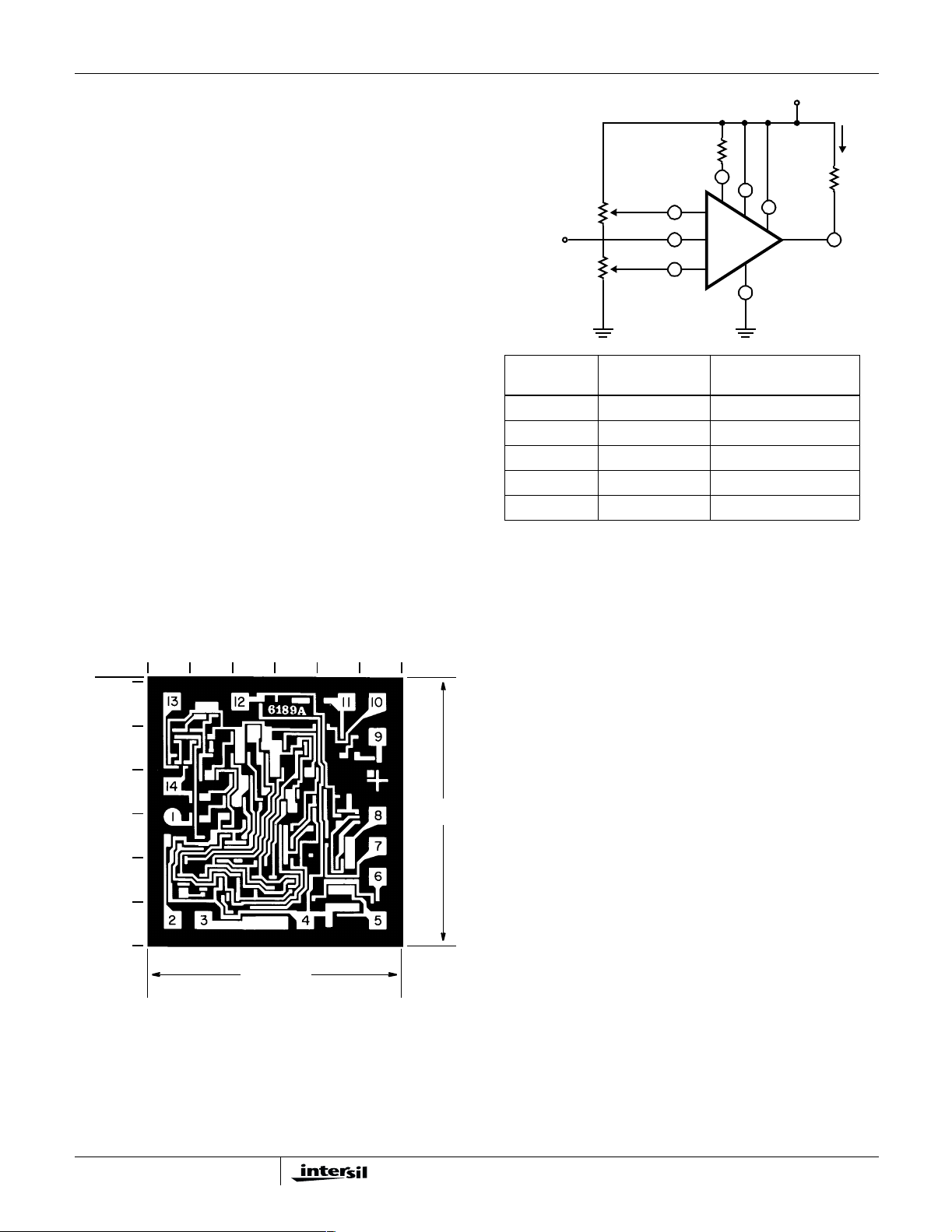
When the signal inpu t voltage of the CA3098 is equal to or
less than t he “low” refer ence vol tag e (LR), cur rent f lows f rom
an external power supply through a load connect ed to
Terminal 3 (“sink” output). This condition is maintained until
the signal inp ut vol tage rises to or exceeds the “high”
reference vol tage (HR), thereby ef fecting a change in the
state of the fli p-flop (memory) such that the output sta ge
interrupts current flow in the external load. This condition, in
turn, is maint ained u n til such time as the signal a g ain
becomes equal to or les s than the “low” reference vol tage.
The CA3098 comparator is unique in that it contains circuit
provisions to permit programmability. This feature provi des
flexibili ty to the designer to optimize quiescent power
consumption, input circuit characteristics, hysteresis, and
additionally permits independent control of the comparator,
namely, pulsin g, strobing, keyin g, squelching, etc.
Programmabili ty is accomplished by means of the bias
current (I
An auxiliary mean s of cont rolling the magnitude of load
current f low at Terminal 3 is pr ovided by “ sinki ng” c urrent i nto
Terminal 5. Figure 1 highlights the operation of the CA3098
when connected as a simple hysteresis switch (Schmitt
trigger).
) supplied to Terminal 2.
BIAS
120kΩ
R
B
2
“HIGH” REF. = 8V
7
INPUT
SIGNAL
E
IN
“LOW” REF. = 4V
INPUT SIGNAL
SEQUENCE
14 ≥ EIN > 0 0
28 ≥ E
3E
28 ≥ EIN > 4 12
14 ≥ E
FIGURE 1. BASIC HYSTERESIS SWITCH (SCHMITT
TRIGGER) AND RESULTANT OUTPUT STATES
8
1
LEVEL
> 4 0
IN
> 8 12
IN
> 0 0
IN
6
5
CA3098
4
OUTPUT VOLTAGE (V)
(TERMINAL 3)
V+ = 12V
3
DC
I
O
R
L
E
O
Metallization Mask Layout
0102030405058
61
60
50
40
30
20
10
0
63 (1.600)
66 (1.676)
Dimensions in parentheses are in millimeters and are derived
from the basic inch dimensions as indicated. Grid graduations
are in mils (10
-3
inch).
The layout repre sents a chip when it is part of the waf er. When
o
the wafer is cut into chips, the cleavage angles are 57
o
with respect to the face of the chip. Therefore, the
of 90
instead
isolated chip is actually 7mils (0.17mm) larger in both
dimensions.
4
 Loading...