

Page 1
查询CA3094供应商
CA3094, CA3094A, CA3094B
Data Sheet April 1999 File Number 598.7
30MHz, High Output Current Operational
Transconductance Amplifier (OTA)
The CA3094 is a differential input power control
switch/amplifier with auxiliary circuit features for ease of
programmability. For example, an error or unbalance signal
can be amplified by the CA3094 to provide an on-off signal or
proportional control output signal up to 100mA. This signal is
sufficient to directly drive high current thyristors, relays, DC
loads, or power transistors. The CA3094 has the generic
characteristics of the CA3080 operational amplifier directly
coupled to an integral Darlington power transistor capable of
sinking or driving currents up to 100mA.
The gain of the differential input stage is proportional to the
amplifier bias current (I
variation of the integrated circuit sensitivity with either digital
and/or analogprogramming signals.For example, at anI
of 100µA, a 1mV change at the input will change the output
from 0 to 100µA (typical).
The CA3094 is intended for operation up to 24V and is
especially useful for timing circuits, in automotive equipment,
and in other applications where operation up to 24V is a
primary design requirement (see Figures 28, 29 and 30 in
Typical Applications text). The CA3094A and CA3094B are
like the CA3094 but are intended for operation up to 36V and
44V, respectively (single or dual supply).
), permitting programmable
ABC
ABC
Features
• CA3094E, M for Operation Up to 24V
• CA3094AT, E, M for Operation Up to 36V
• CA3094BT, M for Operation Up to 44V
• Designed for Single or Dual Power Supply
• Programmable: Strobing, Gating, Squelching, AGC
Capabilities
• Can Deliver 3W (Average)or 10W (Peak) to External Load
(in Switching Mode)
• High Power, Single Ended Class A Amplifier will Deliver
Pow er Output of 0.6W (1.6W Device Dissipation)
• Total Harmonic Distortion (THD) at 0.6W in Class A
Operation 1.4% (Typ)
Applications
• Error Signal Detector: Temperature Control with
Thermistor Sensor; Speed Control for Shunt Wound DC
Motor
• Over Current, Over Voltage, Over Temperature Protectors
• Dual Tracking Power Supply with CA3085
• Wide Frequency Range Oscillator
• Analog Timer
Ordering Information
PART NUMBER
(BRAND)
CA3094AT, BT -55 to 125 8 Pin Metal Can T8.C
CA3094E, AE -55 to 125 8 Ld PDIP E8.3
CA3094M, BM -55 to 125 8 Ld SOIC M8.15
TEMP.
RANGE (oC) PACKAGE
PKG.
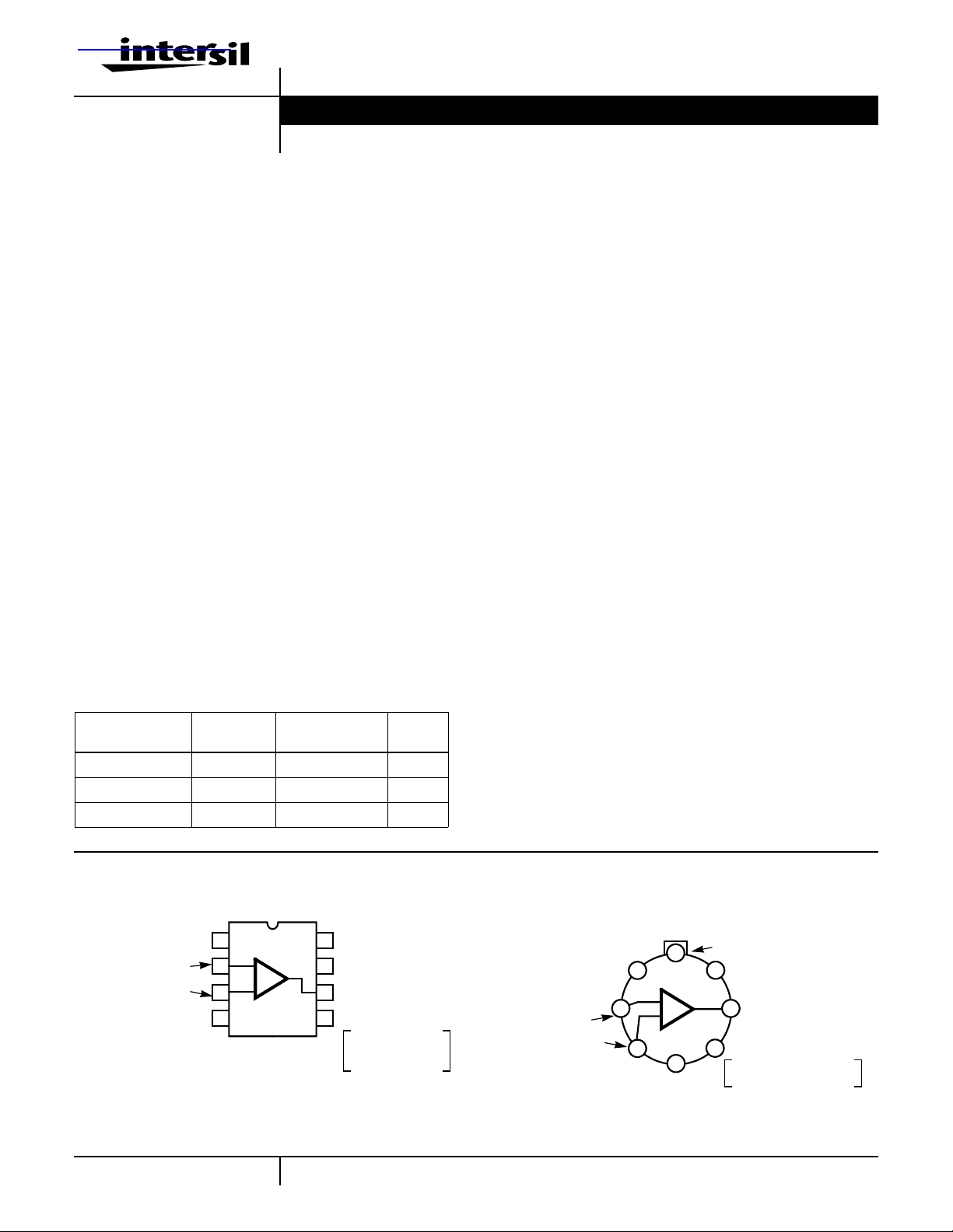
Pinouts
CA3094 (PDIP, SOIC)
TOP VIEW
EXT. FREQUENCY
COMPENSATION
OR INHIBIT INPUT
DIFFERENTIAL
VOLTAGE INPUTS
GND (V- IN DUAL
SUPPLY OPERATION)
1
2
3
4
SINK OUTPUT
8
(COLLECTOR)
V+
7
DRIVE OUTPUT
6
(EMITTER)
5
I
CURRENT
ABC
PROGRAMMABLE
INPUT
(STROBE OR AGC)
NO.
• Level Detector
• Alarm Systems
• Voltage Follower
• Ramp Voltage Generator
• High Power Comparator
• Ground Fault Interrupter (GFI) Circuits
CA3094 (METAL CAN)
TOP VIEW
SINK OUTPUT
(COLLECTOR)
EXT. FREQUENCY
COMPENSATION OR
INHIBIT INPUT
2
DIFFERENTIAL
VOLTAGE INPUTS
GND (V- IN DUAL
SUPPLY OPERATION)
NOTE: Pin 4 is connected to case.
8
1
3
4
TAB
7
V+
DRIVE OUTPUT
6
(EMITTER)
5
CURRENT
I
ABC
PROGRAMMABLE INPUT
(STROBE OR AGC)
3-12
CAUTION: These devices are sensitive to electrostatic discharge; follow proper IC Handling Procedures.
1-888-INTERSIL or 321-724-7143
| Copyright © Intersil Corporation 1999
Page 2
CA3094, CA3094A, CA3094B
Absolute Maximum Ratings Thermal Information
Supply Voltage (Between V+ and V- Terminals)
CA3094 . . . . . . . . . . . . . . . . . . . . . . . . . . . . . . . . . . . . . . . . . 24V
CA3094A . . . . . . . . . . . . . . . . . . . . . . . . . . . . . . . . . . . . . . . . 36V
CA3094B . . . . . . . . . . . . . . . . . . . . . . . . . . . . . . . . . . . . . . . . 44V
Differential Input Voltage (Terminals 2 and 3, Note 1) . . . . . . . . . 5V
DC Input Voltage . . . . . . . . . . . . . . . . . . . . . . . . . . . . . . . . . V+ to V-
Input Current (Terminals 2 and 3) . . . . . . . . . . . . . . . . . . . . . . ±1mA
Amplifier Bias Current (Terminal 5) . . . . . . . . . . . . . . . . . . . . . . 2mA
Average Output Current. . . . . . . . . . . . . . . . . . . . . . . . . . . . . 100mA
Peak Output Current . . . . . . . . . . . . . . . . . . . . . . . . . . . . . . . 300mA
Operating Conditions
Temperature Range. . . . . . . . . . . . . . . . . . . . . . . . . -55oC to 125oC
CAUTION: Stresses above those listed in “Absolute Maximum Ratings” may cause permanent damage to the device. This is a stress only rating and operation of the
device at these or any other conditions above those indicated in the operational sections of this specification is not implied.
NOTES:
1. Exceeding this voltage rating will not damage the device unless the peak input signal current (1mA) is also exceeded.
2. θJA is measured with the component mounted on an evaluation PC board in free air.
Thermal Resistance (Typical, Note 2) θJA (oC/W) θJC (oC/W)
PDIP Package . . . . . . . . . . . . . . . . . . . 130 N/A
SOIC Package . . . . . . . . . . . . . . . . . . . 170 N/A
Metal Can Package . . . . . . . . . . . . . . . 175 100
Maximum Junction Temperature (Metal Can Package) . . . . . . .175oC
Maximum Junction Temperature (Plastic Package) . . . . . . . .150oC
Maximum Storage Temperature Range. . . . . . . . . . -65oC to 150oC
Maximum Lead Temperature (Soldering 10s) . . . . . . . . . . . . 300oC
(SOIC - Lead Tips Only)
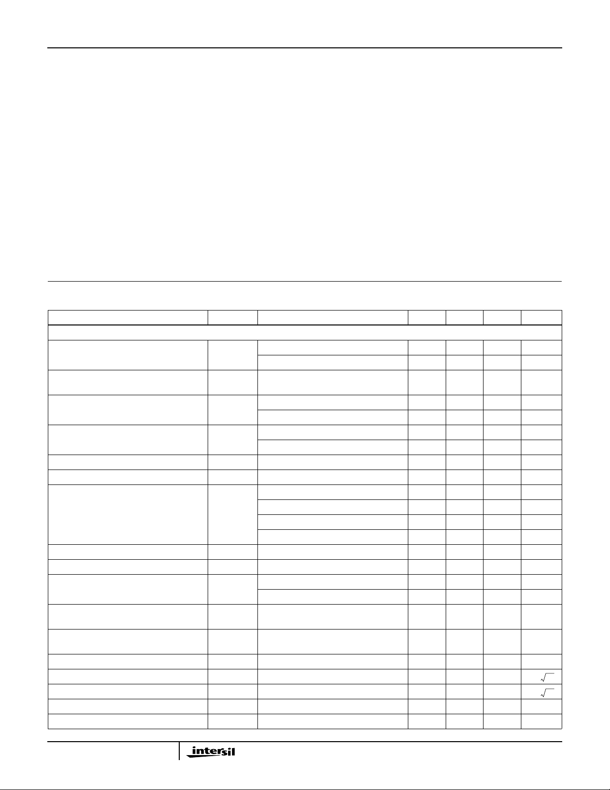
Electrical Specifications T
= 25oC for Equipment Design. Single Supply V+ = 30V, Dual Supply V
A
SUPPLY
= ±15V , I
= 100µA Unless
ABC
Otherwise Specified
PARAMETER SYMBOL TEST CONDITIONS MIN TYP MAX UNITS
INPUT PARAMETERS
Input Offset Voltage V
TA = 25oC - 0.4 5.0 mV
IO
TA = 0oC to 70oC - - 7.0 mV
Input Offset Voltage Change |∆VIO| Change in VIO between I
Input Offset Current I
and I
IO
TA = 25oC - 0.02 0.2 µA
ABC
= 5µA
ABC
= 100µA
- 1 8.0 mV
TA = 0oC to 70oC - - 0.3 µA
Input Bias Current I
TA = 25oC - 0.2 0.50 µA
I
TA = 0oC to 70oC - - 0.70 µA
Device Dissipation P
I
D
= 0mA 8 10 12 mW
OUT
Common Mode Rejection Ratio CMRR 70 110 - dB
Common Mode Input Voltage Range V
ICR
V+ = 30V (High) 27 28.8 - V
V- = 0V (Low) 1.0 0.5 - V
V+ = 15V 12 13.8 - V
V- = -15V -14 -14.5 - V
Unity Gain Bandwidth f
Open Loop Bandwidth at -3dB Point BW
Total Harmonic Distortion
THD PD = 220mW - 0.4 - %
(Class A Operation)
Amplifier Bias Voltage
V
ABC
IC = 7.5mA, VCE = 15V, I
T
OLIC
= 7.5mA, VCE = 15V, I
= 500µA - 30 - MHz
ABC
= 500µA - 4 - kHz
ABC
PD = 600mW - 1.4 - %
- 0.68 - V
(Terminal 5 to Terminal 4)
Input Offset Voltage Temperature
∆VIO/∆T-4-µV/oC
Coefficient
Power Supply Rejection ∆VIO/∆V - 15 150 µV/V
1/F Noise Voltage E
1/F Noise Current I
Differential Input Resistance R
Differential Input Capacitance C
f = 10Hz, I
N
f = 10Hz, I
N
I
I
I
= 20µA 0.50 1.0 - MΩ
ABC
f = 1MHz, V+ = 30V - 2.6 - pF
= 50µA - 18 -
ABC
= 50µA - 1.8 -
ABC
nV/ Hz
pA/ Hz
3-13
Page 3
CA3094, CA3094A, CA3094B
Electrical Specifications T
= 25oC for Equipment Design. Single Supply V+ = 30V, Dual Supply V
A
Otherwise Specified (Continued)
PARAMETER SYMBOL TEST CONDITIONS MIN TYP MAX UNITS
OUTPUT PARAMETERS (Differential Input Voltage = 1V)
Peak Output Voltage
(Terminal 6)
Peak Output Voltage
(Terminal 6)
Peak Output Voltage
(Terminal 8)
Peak Output Voltage
(Terminal 8)
Collector-to-Emitter Saturation Voltage
(Terminal 8)
Output Leakage Current
With Q13 “ON” VOM+ V+ = 30V, RL = 2kΩ to GND 26 27 - V
With Q13 “OFF” VOM- - 0.01 0.05 V
Positive VOM+ V+ = 15V, V- = -15V, RL = 2kΩ to -15V 11 12 - V
Negative VOM- - -14.99 -14.95 V
With Q13 “OFF” VOM+ V+ = 30V, RL = 2kΩ to 30V 29.95 29.99 - V
With Q13 “ON” VOM- - 0.040 - V
Positive VOM+ V+ = 15V, V- = -15V,
Negative VOM- - -14.96 - V
V
CE(
RL = 2kΩ to 15V
V+ = 30V, IC = 50mA, Terminal 6
)
SAT
Grounded
V+ = 30V - 2 10 µA
(Terminal 6 to Terminal 4)
Composite Small Signal Current Transfer
Ratio (Beta) (Q12 and Q13)
Output Capacitance Terminal 6 C
Terminal 8 - 17 - pF
h
FE
V+ = 30V, VCE = 5V, IC = 50mA 16,000 100,000 -
f = 1MHz, All Remaining Terminals Tied
O
to Terminal 4
TRANSFER PARAMETERS
Voltage Gain A V+ = 30V, I
RL = 2kΩ
Forward Transconductance to
Terminal 1
Slew Rate (Open
Loop)
Positive Slope SR I
Negative Slope - 50 - V/µs
Unity Gain (Non-Inverting Compensated) I
g
M
= 500µA, RL = 2kΩ - 500 - V/µs
ABC
= 500µA, RL = 2kΩ - 0.70 - V/µs
ABC
= 100µA, ∆V
ABC
OUT
= 20V,
SUPPLY
= ±15V , I
= 100µA Unless
ABC
14.95 14.99 - V
- 0.17 0.80 V
- 5.5 - pF
20,000 100,000 - V/V
86 100 - dB
1650 2200 2750 µS
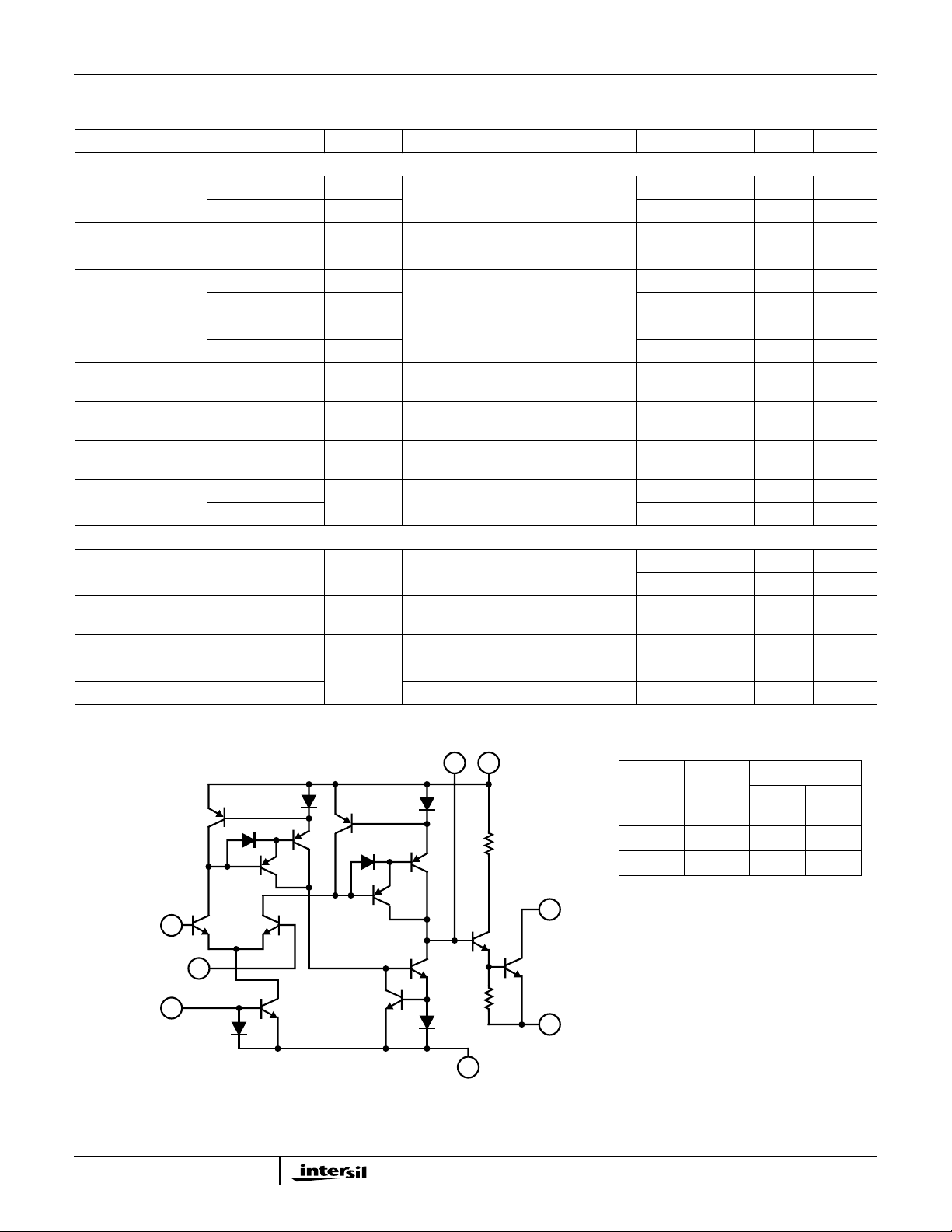
Schematic Diagram
Q
4
DIFFERENTIAL
VOLTAGE
DIFFERENTIAL
AMPLIFIER
BIAS INPUT
INPUT
VOLTAGE
INPUT
I
ABC
2
Q
1
3
5
D
1
COMPENSATION OR INHIBIT INPUT
D
2
Q
2
EXTERNAL FREQUENCY
D
3
Q
7
Q
6
Q
5
Q
3
D
4
Q
Q
11
3-14
V+
71
D
5
R
1
R
47kΩ
4
2kΩ
8
“SINK”
Q
OUTPUT
12
Q
13
2
6
“SOURCE”
(DRIVE)
V-
OUTPUT
Q
8
9
Q
10
D
6
OUTPUT
MODE
“Source” 6 2 3
“Sink” 8 3 2
OUTPUT
TERM
INPUTS
INV
NON-
INV
Page 4
CA3094, CA3094A, CA3094B
Operating Considerations
The “Sink” Output (Terminal 8) and the “Drive” Output
(Terminal 6) of the CA3094 are not inherently current (or
power) limited. Therefore, if a load is connected between
Terminal 6 and Terminal 4 (V- or Ground), it is important to
connect a current limiting resistor between Terminal 8 and
Terminal 7 (V+) to protect transistor Q13 under shorted load
conditions. Similarly,if a load is connected between Terminal
8 and Terminal 7 (V+), the current limiting resistor should be
connected between Terminal 6 and Terminal 4 or ground. In
circuit applications where the emitter of the output transistor
is not connected to the most negative potential in the
system, it is recommended that a 100Ω current limiting
resistor be inserted between Terminal 7 and the V+ supply.
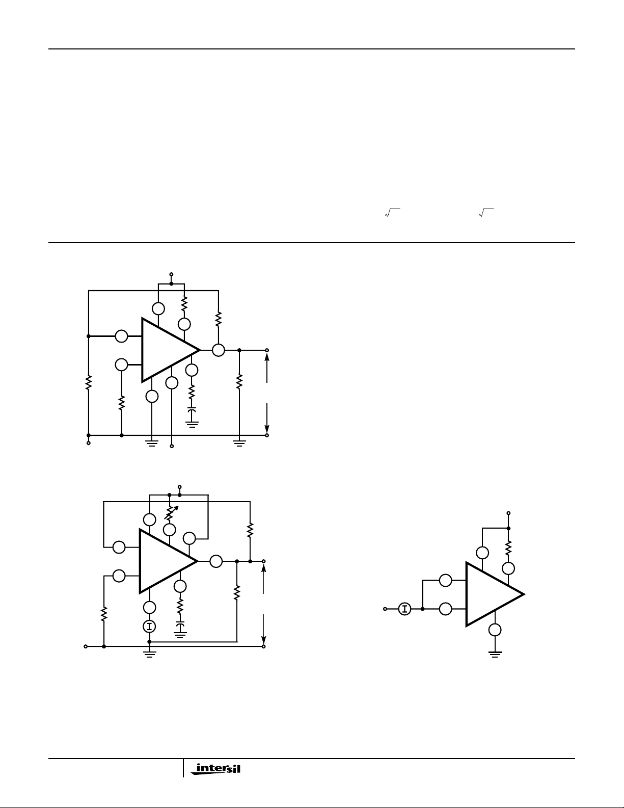
Test Circuits
30V
300kΩ
1kΩ
100pF
6
10kΩ
9.9kΩ
E
OUT
5
1
8
30V
100Ω
15V
100Ω
7
2
CA3094
3
4
1/F Noise Measurement Circuit
When using the CA3094, A, or B audio amplifier circuits, it is
frequently necessary to consider the noise performance of the
device.Noise measurements are made in the circuit shown in
Figure 20. This circuit is a 30dB, non-inverting amplifier with
emitter follower output and phase compensation from
Terminal 2 to ground. Source resistors (R
) are set to 0Ω or
S
1MΩ for E noise and I noise measurements, respectiv ely.
These measurements are made at frequencies of 10Hz,
100Hz and 1kHz with a 1Hz measurement bandwidth. Typical
values for 1/f noise at 10Hz and 50µA I
EN18nV Hz⁄= IN1.8pA Hz⁄=
NOTES:
3. Input Offset Voltage: .
4. For Power Supply Rejection Test: (1) vary V+ by -2V; then (2)
vary V- by +2V.
5. Equations:
(1)
V+ Rejection
(2)
V- Rejection
6. Power Supply Rejection: .
and .
E
IO
200
dB()20
200
-----------------=
OUT
100
V
E0OUT E1OUT–
------------------------------------------------ -=
E0OUT E2OUT–
------------------------------------------------ -=
are:
ABC
1
---------------------------------------------
log=
V
REJECTION
†
† Maximum Reading of Step 1 or Step 2
FIGURE 1. INPUT OFFSET VOLTAGE AND POWER SUPPLY REJECTION TEST CIRCUIT
30V
R
5
1
8. I
ABC
8
220Ω
0.001µF
OS
6
150kΩ
--------------------------------=
10
E
6
15V
NOTES:
7. P
DISSIPATION
2
3
1MΩ
= (V+)(I)
7
CA3094
4
FIGURE 2. INPUT OFFSET CURRENT TEST CIRCUIT
OUT
VOLTS
---------------------
AMPS
1MΩ
E
OUT
30V
300kΩ
5
4
15V
NOTE: I
7
2
-
CA3094A
+
3
I
-- -=
I
2
FIGURE 3. INPUT BIAS CURRENT TEST CIRCUIT
3-15
Page 5
Test Circuits (Continued)
30V
100Ω
100Ω
V
CMR
0.8V TO 27.2V
15V
2
3
9.9kΩ
200Ω
FIGURE 4. COMMON MODE RANGE AND REJECTION RATIO TEST CIRCUIT
7
-
CA3094
+
1
1kΩ
100pF
4.7kΩ
CA3094, CA3094A, CA3094B
10kΩ
8
6
4
10kΩ
E
OUT
NOTES:
9. .
CMRR
100 26V×
=
--------------------------------------------
E
–
2OUTE1OUT
10. Input Voltage Range for CMRR = 1V to 27V.
11. .
CMRR (dB) 20
100 26V×
log=
--------------------------------------------
E
2OUTE1OUT
–
3.6kΩ
120Ω
I
ABC
R
S
(NOTE)
3
R
S
(NOTE)
I
(µA)
ABC
C
COMP
(pF)
50
50 50
5
7
2
-
CA3094A
+
4
1
C
C
NOTE:
RS= 1MΩ
(1/F Noise Current Test).
RS= 0Ω
(1/F Noise Voltage Test).
500 500
FIGURE 5. 1/F NOISE TEST CIRCUIT
+15V
8
6
+15V
500Ω
3kΩ
-15V
OUTPUT
(RMS)
+15V
7
8
6
OUTPUT
R
= 2kΩ
L
-15V
10kΩ
91Ω
100Ω 10Ω
10kΩ
10Ω
R
(Ω)
+15V-15V
R
S
5
I
ABC
2
-
CA3094A
3
+
4
I
S
ABC
(µA)
56K 500
560K 50
56M 5
FIGURE 6. OPEN LOOP GAIN vs FREQUENCY TEST CIRCUIT
+15V
I
ABC
5
2V
0V
2
13kΩ
3
15kΩ
-15V
7
-
CA3094A
+
4
FIGURE 7. OPEN LOOP SLEW RATE vs I
3-16
8
6
2kΩ
TEST CIRCUIT
ABC
E
OUT
56kΩ
5
±10V
10kΩ
2
3
220Ω
0.001µF
-
CA3094A
+
1
7
8
4
-15V
10kΩ
6
2kΩ
FIGURE 8. SLEW RATEvs NON-INVERTING UNITY GAIN
TEST CIRCUIT
E
OUT
Page 6

Test Circuits (Continued)
CA3094, CA3094A, CA3094B
120VAC
51Ω
+15V
56kΩ
5
-
CA3094A
+
1
C
7
4
C
C
-15V
R
2
2
R
1
3
R
CLOSED
LOOP GAIN
(dB)
R
(kΩ)
1
(kΩ)
010
20 10 1 10
40 1 0.1 10
R
8
1
29V
0
27V
0
R
LOAD
R
1
R
2
R
3
R
4
3V
Time = 1 hr.
S2 Set to R
MT
MT
E
OUT
2
1
4
V+ = 30V
R
5
S
R
2kΩ
3
(NOTE 12)
R
OUTPUT
COMMON
8
6
1
R
6
D
1
7
C
NOTES:
7
+
3
CA3094A
-
2
4
1
S
2
8
5
6
S
12. C1 = 0.5µF
D1 = 1N914
R1 = 0.51MΩ = 3 min.
R2 = 5.1MΩ = 30 min.
R
2
R
3
(kΩ)
∞
10
R3 = 22MΩ = 2 hrs.
R4 = 44MΩ = 4 hrs.
R5 = 1.5kΩ
R6 = 50kΩ
R7 = 5.1kΩ
3
6
R8 = 1.5kΩ
13. Potentiometer required for initial time set to permit device interconnecting. Time variation with temperature <0.3%/oC.
FIGURE 9. PHASE COMPENSATION TEST CIRCUIT FIGURE 10. PRESETTABLE ANALOG TIMER
Application Information
For additional application information, refer to
Application Note AN6048, “Some Applications of a
Programmable Power/Switch Amplifier IC” and AN6077
“An IC Operational Transconductance Amplifier (OTA)
with Power Capability”.
Design Considerations
The selection of the optimum amplifier bias current (I
depends on:
1. The Desired Sensitivity - The higher the I
, the higher
ABC
thesensitivity, i.e., a greaterdrivecurrent capability at the
output for a specific voltage change at the input.
2. Required Input Resistance - The lower the I
ABC
er the input resistance.
)
ABC
,the high-
If the desired sensitivity and required input resistance are
not known and are to be experimentally determined, or the
anticipated equipment design is sufficiently flexible to
tolerate a wide range of these parameters, it is
recommended that the equipment designer begin his
calculations with an I
of 100µA, since the CA3094 is
ABC
characterized at this value of amplifier bias current.
The CA3094 is extremely versatile and can be used in a
wide variety of applications.
3-17
Page 7

Typical Applications
CA3094, CA3094A, CA3094B
Z
1
Z
2
-
E
IN
=
Z
------ -
Z
E
OUT
----------------- f
here depends on the characteristics of Z1and Z
E
IN
CA3094
+
2
1
NOTE: In single-ended output operation, the CA3094 may require a pull up or pull down resistor.
FIGURE 11A. INVERTING OP AMP FIGURE 11B. NON-INVERTING MODE, AS A FOLLOWER
FIGURE 11. APPLICA TION OF THE CA3094
V+ = 18V
S
VOLTAGE A
2/3V+
0
+18
0
VOLTAGE AT
TERMINAL 8
1
R
I
I
A
1N914
12V
C
TIME DELAY (s) = RC (APPROX.)
R
1
100kΩ
R
2
220kΩ
R
ABC
220kΩ
2
3
5
+
CA3094
-
4
E
OUT
(NOTE)
7
8
6
2
2kΩ
PULL UP
E
OUT
+
E
IN
Where E
CA3094
-
OUT=EIN
E
OUT
(NOTE)
Problem: To calculate the maximum value of R required to
switch a 100mA output current comparator
18V
Given:
I
ABC
II = 500nA at I
5µA,= R
ABC
= 100µA (from Figure 3)
ABC
3.6MΩ
≈=
-----------
5µA
II=5µA can be determined by drawing a line on Figure 3 through
I
= 100µA and IB= 500nA parallel to the typical TA=25oC
ABC
curve.
Then: II = 33nA at I
R
MAX
R
MAX
† Ratio of I
of I
18V 12V–
--------------------------- - 180MΩ at TA25oC== =
33nA
180MΩ 23†⁄× 120MΩ at T
at TA=25oCtoIIat TA= -55oC for any given value
I
ABC
ABC
= 5µA
55oC–===
A
INPUT
FIGURE 12. RC TIMER
V+
A
0
V+
R
100
kΩ
270
B
100
kΩ
1N914
100
kΩ
kΩ
100
kΩ
0.01µF
A
12V
DC
1
1MΩ
D
R
2
2.2MΩ
C
R
3
1MΩ
7
+
3
CA3094
-
2
4
220kΩ
C
8
5
6
1
0.5µF
E
R
2kΩ
E
LOAD
OUT
0
B
0
C
D
0
V+
E
0
3
/4V+
On a negative going transient at input (A), a negative
pulse at C will turn “on” the CA3094, and the output (E)
will go from a low to a high level.
At the end of the time constant determined by C1,R1,
R2,R3, the CA3094 will return to the “off” state and the
output will be pulled low by R
. This condition will
LOAD
be independent of the interval when input (A) returns
to a high level.
FIGURE 13. RC TIMER TRIGGERED BY EXTERNAL NEGATIVE PULSE
3-18
Page 8

Typical Applications (Continued)
+
10kΩ MIN
R
1MΩ MAX
2.7MΩ
5V
DC
C
330kΩ
C
-
0.01µF
PAPER OR
MYLAR™
7
3
-
CA3094
2
+
1
4
TYPE
1N914
5
8
6
CA3094, CA3094A, CA3094B
510Ω
47kΩ
20kΩ
E
OUT
1N914
47kΩ
100kΩ
2
3
C
7
+
CA3094
-
5
+15V
1kΩ
8
OUTPUT
6
4
NOTES:
14. R = 1MΩ, C = 1µF.
E
OUT
2ms
120s
15. Time Constant: t ≈ RC x 120.
LINE
16. Pulse Width: ω≈ K(C1/C).
FIGURE 14. FREE RUNNING PULSE GENERATOR
27kΩ
50kΩ
27kΩ
R
100kΩ
P
C
R
100kΩ
560pF
300kΩ
2
3
5
+
CA3094A
-
CURRENT INPUT
OR
VOLTAGE INPUT
R
FIGURE 15. CURRENT OR VOLTAGE CONTROLLED OSCILLA T OR
15V
7
6
-15V
1kΩ
OUTPUT
≈ 5kHz
f
OUT
8
R
2
30V
510Ω
LED
7
8
NOTE:
51kΩ
R
1
4.3kΩ
f
OUT
C 1000pF
---------------------------------------------------=
2RC()ln
6
4
If: R2 = 3.08R1,
300kΩ
R
100kΩ
2
3
1
2R
---------- - 1+
R
f
OUT
1
2
5
+
CA3094A
-
4
1
-------- -=
RC
FIGURE 16. SINGLE SUPPLY ASTABLE MULTIVIBRATOR FIGURE 17. DUAL SUPPLY ASTABLE MULTIVIBRATOR
3-19
Mylar™ is a trademark of E.I. Dupont de Nemours
Page 9

Typical Applications (Continued)
CA3094, CA3094A, CA3094B
+15V
150kΩ
300kΩ
5
7
-
CA3094A
+
6
4
INPUT
R
100kΩ
R (NOTE 17)
51kΩ
1
3
2
R
2
100kΩ
NOTES:
R1R
2
17. .
18. .
-------------------- -=
R
R1R2+
Threshold± Supply±[]
=
-------------------- -
R1R2+
R
1
FIGURE 18A. DUAL SUPPLY FIGURE 18B. SINGLE SUPPLY
FIGURE 18. COMPARATORS (THRESHOLD DETECTORS) DUAL AND SINGLE SUPPLY TYPES
+15V
2kΩ
8
-15V
OUTPUT
INPUT
NOTES:
19. .
20. .
51kΩ
R
A
200kΩ
R
B
200kΩ
100kΩ
Upper Threshold V+[]
Lower Threshold V+[]
5
7
6
R
R1R
---------------------
R1RA+
R1R
---------------------
R1RB+
R
1RB
---------------------
R1RB+
8
B
A
+
B
+
3
-
CA3094
2
+
4
R
1
----------------------------------------- -
=
----------------------------------------- -
=
2kΩ
OUTPUT
R
B
R
A
TYPE
D1201F
PTC TEMP.
50µF
50V
SENSOR
75kΩ
68kΩ
10kΩ
75kΩ
TEMP.
SET
R
75kΩ
+
10Ω
-
117V
60Hz
FOR NTC SENSOR, INTERCHANGE POSITION OF SENSOR AND .
26V
60Hz
FIGURE 19. TEMPERATURE CONTROLLER
1N914
R
1.5MΩ 1N914
330kΩ
7
2
CA3094
3
1.5kΩ
5
8
4
NOTE: All Resistors are 1/2W.
HEATER
MT
2
1kΩ
MT
6
G
0.01µF
1
3-20
Page 10

Typical Applications (Continued)
CA3094, CA3094A, CA3094B
V+ INPUT
(NOTE 21)
V- INPUT
(NOTE 22)
2
3
0.0056µF
5.1kΩ
CA3085A
VOLTAGE REG.
4
REF.
1.6V
200kΩ
100Ω
+
2
3
6 7
0.01µF
1
5
CA3094A
-
6
4
10kΩ
1.5kΩ
10kΩ
±1%
NOTE 23
1
5.6Ω
8
R
5kΩ
+15V REG.
OUTPUT
NOTES:
21. V+ Input Range = 19V to 30V for 15V output.
22. V- Input Range = -16V to -30V for -15V output.
COMMON
RETURN
23. Max I
= ±100mA.
OUT
24. Regulation:
∆V
OUT
∆V
OUT
OUT
OUT
Initial()[]∆V
Initial()
100× 0.075% V
100× 0.075% V⁄==
IN
OUT
from 1mA to 50mA)
(I
L
Max Line
7
0.03µF
Max Load
8
-15V REG.
OUTPUT
-----------------------------------------------------------
V
---------------------------------------
==
V
200mV
RANGE
R
47kΩ
(NOTE 27)
L
C
0.02µF
C
0.1µF
(NOTE 28)
10kΩ
±1%
FIGURE 20. DUAL VOLTAGE TRACKING REGULATOR
CIRCUIT TRIPS ON POSITIVE
36V
1mA
33kΩ
+3V
I
ABC
3
100kΩ
2
10µA
3.3MΩ
5
-
CA3094B
+
4
R
TRIP
200
Ω
3.3
kΩ
47kΩ
2
7
6
I
A
20µA
100Ω
8
CIRCUIT
BREAKER
CONTROL
SOLENOID
I
LOAD
3
VOLTS
NOTES:
25. Differential current sensor provides 60mV signal ≈ 5mA of
26. All Resistors are 1/2 Watt, ±10%.
27. RC selected for 3dB point at 200Hz.
PEAKS WILL SWITCH WITHIN
1.5 CYCLES
60mV
TYPICAL
GROUND FAULT
SIGNAL 60Hz
t
unbalance (Trip) current.
VOLTAGE BETWEEN
TERMINALS 2 AND 4
VOLTAGE BETWEEN
TERMINALS 3 AND 4
(ADJUSTABLE WITH
R
)
TRIP
28. C2 = AC bypass.
29. Offset adj. included in R
TRIP
.
30. Input impedance from 2 to 3 = 800kΩ.
1kΩ
0.001µF
31. With no input signal Terminal 8 (output) at 36V.
FIGURE 21. GROUND FAULT INTERRUPTER (GFI) AND WAVEFORMS PERTINENT TO GROUND FAULT DETECTOR
3-21
Page 11

Typical Applications (Continued)
CA3094, CA3094A, CA3094B
“BOOST”
0.12µF
68Ω
INPUT
25µF
+
(CW)
1800Ω
0.001µF
C
1
(NOTES
32, 33)
TREBLE
15kΩ
0.2µF
1kΩ
“BOOST”
“CUT”
(CCW)
0.001µF
R
1
(CW)
VOLUME
2
3
100kΩ
BASS
0.01µF
5600Ω
5µF
680
kΩ
“CUT”
(CCW)
+
7
+
CA3094B
-
4
5
0.02µF
820Ω
0.47
µF
10kΩ
1
6
6.8pF
8 LEAD
TO-5
1Ω
220Ω
1W
220Ω
1W
30Ω
27Ω
8
COMPENSATION
15µF
+
Q
2N6292
†
THERMAL
NETWORK†
2
Q
1
Q
3
C
2
0.47µF
JUMPER (NOTES 32, 33)
+
2N6292
0.47Ω
0.47Ω
2N6107
4700µF
+
D
- D4 1N5391
1
V+
V-
4700
µF
330Ω
47Ω
D
1
D
2
D
3
D
4
3µH
22Ω
R
2
1.8MΩ
(NOTES 32, 33)
†OPTIONAL THERMAL
COMPENSATION
NETWORK
STANCOR
NO. P-8609
OR EQUIVALENT
(120VAC TO
26.8VCT AT 1A)
R
L
8Ω
8.2Ω
1N5391
120V
60Hz
TYPICAL PERFORMANCE DATA FOR 12W AUDIO AMPLIFIER CIRCUIT
Power Output (8Ω load, Tone Control Set at “Flat”)
Music (at 5% THD, Regulated Supply). . . . . . . . . . . . . . . . . . 15W
Continuous (at 0.2% IMD, 60Hz and 2kHz
Mixed in a 4:1 Ratio, Unregulated Supply)
See Figure 8 in AN6048. . . . . . . . . . . . . . . . . . . . . . . . . . . . . 12W
Total Harmonic Distortion
At 1W, Unregulated Supply . . . . . . . . . . . . . . . . . . . . . . . . .0.05%
At 12W, Unregulated Supply . . . . . . . . . . . . . . . . . . . . . . . .0.57%
Input Resistance . . . . . . . . . . . . . . . . . . . . . . . . . . . . . . . . . . .250kΩ
Tone Control Range. . . . . . . . . . . . . . . . . . .See Figure 9 in AN6048
NOTES:
32. For standard input: Short C2;R1= 250kΩ,C1= 0.047µF; remove
R2.
33. For ceramic cartridge input: C1= 0.0047µF, R1= 2.5MΩ, remove
jumper from C2; leave R2.
Voltage Gain . . . . . . . . . . . . . . . . . . . . . . . . . . . . . . . . . . . . . . .40dB
Hum and Noise (Below Continuous Power Output). . . . . . . . . .83dB
FIGURE 22. 12W AUDIO AMPLIFIER CIRCUIT FEATURINGTRUE COMPLEMENTARY SYMMETRY OUTPUT STAGE WITH CA3094 IN
DRIVER STAGE
3-22
Page 12

Typical Performance Curves
5
V+ = +15V, V- = -15V
4
3
2
1
0
-1
-2
-3
-4
-5
INPUT OFFSET VOLTAGE (mV)
-6
-7
-8
0.1 1 10 100 1000
o
25
C
-55oC
o
70
C
o
90
C
125oC
AMPLIFIER BIAS CURRENT (µA)
CA3094, CA3094A, CA3094B
3
10
125
90oC
70oC
o
25
-55oC
o
C
C
V+ = +15V, V- = -15V
2
10
1
10
1
0.1
INPUT OFFSET CURRENT (nA)
0.01
0.1 1.0 10 100 1000
o
C
-55
o
C
25
125oC
AMPLIFIER BIAS CURRENT (µA)
FIGURE 23. INPUT OFFSET VOLTAGE vs AMPLIFIER BIAS
CURRENT (I
4
10
V+ = +15V, V- = -15V
3
10
2
10
1
10
3
1.0
INPUT BIAS CURRENT (nA)
0.1
0.1 1 10 100 1000
AMPLIFIER BIAS CURRENT (µA)
, TERMINAL 5)
ABC
0.88µA
125oC
25oC
o
-55
C
FIGURE 25. INPUT BIAS CURRENT vs AMPLIFIER BIAS
CURRENT (I
4
10
V+ = +15V, V- = -15V
3
10
2
10
1
10
125oC
1.0
AMPLIFIER SUPPLY CURRENT (µA)
0.1
0.1 1.0 10 100 1000
25oC
o
C
-55
AMPLIFIER BIAS CURRENT (µA)
, TERMINAL 5)
ABC
TA = 125oC
o
25
C
-55oC
FIGURE 27. AMPLIFIER SUPPLY CURRENT vs AMPLIFIER
BIAS CURRENT (I
, TERMINAL 5)
ABC
FIGURE 24. INPUT OFFSET CURRENT vs AMPLIFIER BIAS
CURRENT (I
5
10
TA = 25oC
4
10
3
10
2
10
1
DEVICE DISSIPATION (µW)
10
1
0.1 1.0 10 100 1000
AMPLIFIER BIAS CURRENT (µA)
, TERMINAL 5)
ABC
V+ = +15V, V- = -15V
V+ = +6V, V- = -6V
V+ = +3V, V- = -3V
FIGURE 26. DEVICE DISSIPATION vs AMPLIFIER BIAS
CURRENT (I
15.0
V+ = +15V, V- = -15V
14.5
= 25oC
T
A
14.0
13.5
13.0
0
-13.0
-13.5
-14.0
-14.5
COMMON MODE INPUT VOLTAGE (V)
-15.0
0.1 1.0 10 100 1000
AMPLIFIER BIAS CURRENT (µA)
, TERMINAL 5)
ABC
V+
CMR
V-
CMR
FIGURE 28. COMMON MODE INPUT VOLTAGEvs AMPLIFIER
BIAS CURRENT (I
, TERMINAL 5)
ABC
3-23
Page 13

CA3094, CA3094A, CA3094B
Typical Performance Curves (Continued)
50
V+ = +15V, V- = -15V
RS = 0Ω, TA = 25oC
45
FOR TEST CIRCUIT, SEE FIGURE 20
40
35
30
25
20
1/F NOISE VOLTAGE (nV/√Hz)
15
10
1
10
50µA
I
= 5µA
ABC
500µA
2
10
FREQUENCY (Hz)
3
10
100
V+ = +15V, V- = -15V
= 1MΩ, TA = 25oC
R
S
FOR TEST CIRCUIT, SEE FIGURE 20
10
1.0
1/F NOISE CURRENT (pA/√Hz)
0.1
1
10
5µA
I
= 500µA
ABC
50µA
2
10
FREQUENCY (Hz)
FIGURE 29. 1/F NOISE VOLTAGE vs FREQUENCY FIGURE 30. 1/F NOISE CURRENT vs FREQUENCY
10000
FORCED BETA = 10
T
A
1000
= 25oC
1000
V+ = 20V, VCE = 10V
T
= 25oC
A
100
3
10
100
COLLECTOR-TO-EMITTER
SATURATION VOLTAGE (mV)
10
1 10 100 1000
COLLECTOR CURRENT (mA)
FIGURE 31. COLLECTOREMITTER SATURATION VOLTAGE vs
COLLECTOR CURRENT OF OUTPUT
TRANSISTOR (Q13)
110
100
90
80
5µA
70
PHASE ANGLE
60
(I
50
40
30
20
V+ = +15V, V- = -15V, RL = 2kΩ
10
OPEN LOOP VOLTAGE GAIN (dB)
(TERMINAL 6 TO V-), T
0
FOR TEST CIRCUIT, SEE FIGURE 21
-10
110
ABC
10
1
50µA
= 500µA)
10210
FREQUENCY (Hz)
= 25oC
A
3
I
= 500µA
ABC
4
10510610
0
-50
-100
-150
-200
7
PHASE ANGLE (DEGREES)
10
COMPOSITE DC BETA (Q12, Q13)
1
1 10 100 1000
COLLECTOR CURRENT (mA)
FIGURE32. COMPOSITE DCBETAvs COLLECTORCURRENT
OF DARLINGTON CONNECTED OUTPUT
TRANSISTORS (Q12, Q13)
5
10
V+ = +15V, V- = -15V
4
10
3
10
2
10
1
10
FORWARD TRANSCONDUCTANCE (µS)
1
0.1 1.0 10 100 1000
AMPLIFIER BIAS CURRENT (µA)
-55oC
25oC
125oC
FIGURE 33. OPEN LOOP VOLTAGE GAIN vs FREQUENCY FIGURE 34. FORWARD TRANSCONDUCTANCE vs
AMPLIFIER BIAS CURRENT
3-24
Page 14

CA3094, CA3094A, CA3094B
Typical Performance Curves (Continued)
100
V+ = +15V, V- = -15V, TA = 25oC
FOR TEST CIRCUIT, SEE FIGURE 22
10
1.0
SLEW RATE (V/µs)
0.1
1 10 100 1000
AMPLIFIER BIAS CURRENT (µA)
100
V+ = +15V, V- = -15V, I
FOR TEST CIRCUIT, SEE FIGURE 23
10
1.0
SLEW RATE (V/µs)
0.1
0204060
CLOSED LOOP VOLTAGE GAIN (dB)
= 500µA, TA = 25oC
ABC
80 100
FIGURE 35. SLEW RATE vs AMPLIFIER BIAS CURRENT FIGURE 36. SLEW RATE vs CLOSED LOOP VOLTAGE GAIN
1000
100
80
60
40
20
10
8
6
4
2
PHASE COMPENSATION CAPACITANCE (pF)
1
0204050
V+ = +15V , V- = -15V, I
CLOSED LOOP VOLTAGE GAIN (dB)
100mV OUTPUT SIGNAL WITH
10% OVERSHOOT
FOR PHASE COMPENSATION
TEST CIRCUIT, SEE FIGURE 24
R
C
= 500mA, TA = 25oC
ABC
C
C
1000
800
600
400
200
PHASE COMPENSATION RESISTANCE (Ω)
60 703010
FIGURE 37. PHASE COMPENSATION CAPACITANCE AND RESISTANCE vs CLOSED LOOP VOLTAGE GAIN
3-25
 Loading...