Intersil Corporation CA3082M96, CA3082, CA3081M, CA3081F, CA3081 Datasheet

T
®
P
E
T
E
L
O
S
B
O
B
I
S
S
O
P
A
R
O
F
c
1
t
c
a
t
n
o
I
-
8
8
8
-
e
T
r
u
o
S
R
E
T
N
B
U
S
E
L
a
c
i
n
h
c
w
r
o
L
I
C
U
D
O
R
T
I
T
S
p
u
S
l
Data Sheet May 2001 File Numbe r 480.6
n
i
.
w
w
R
P
E
T
U
e
C
t
r
o
p
t
o
c
.
l
i
s
r
e
T
C
U
D
O
t
a
r
e
t
n
c
s
t
/
m
CA3081, CA3082
General Purpose High Current NPN
Transistor Arrays
CA3081 and CA3082 consist of seven high current (to
100mA) silico n NPN trans is tors on a common monolithic
substrate. The CA3081 is connected in a common emitter
configuration and the CA3082 is connected in a common
collector configuration.
The CA3081 and CA3082 are capable of dir ectly driving
seven segment displays, and light emi tt ing diode (LED)
displays. These types are also well suited for a variety of
other drive applications, inc luding relay control and thyristor
firing.
Part Number Information
PART NUMBER
(BRAND)
CA3081 -55 to 125 16 Ld PDIP E16.3
CA3081F -55 to 125 16 Ld CERDIP F16.3
CA3081M
(3081)
CA3082 -55 to 125 16 Ld PDIP E16.3
CA3082M
(3082)
CA3082M96
(3082)
TEMP.
RANGE (
o
C) PACKAGE
-55 to 125 16 Ld SOIC M16.15
-55 to 125 16 Ld SOIC M16.15
-55 to 125 16 Ld SOIC Tape
and Reel
PKG.
M16.15
NO.
Features
• CA3081 - Common Emitter Array
• CA3082 - Common Collector Array
• Directly Drive Seven Segment Incandescent Displays an d
Light Emitting Diode (LED) Display
• 7 Transistors Permit a Wide Range of Appl ications in
Either a Common Emitter ( C A3081) or Common Collector
(CA3082) Configurati on
•High I
• Low V
. . . . . . . . . . . . . . . . . . . . . . . . . . . . 100mA (Max)
C
(at 50mA) . . . . . . . . . . . . . . . . . . 0.4V (Typ)
CESAT
Applications
•Drivers for
- Incandescent Display Devices
- LED Displays
• Relay Control
• Thyristor Firing
Pinouts
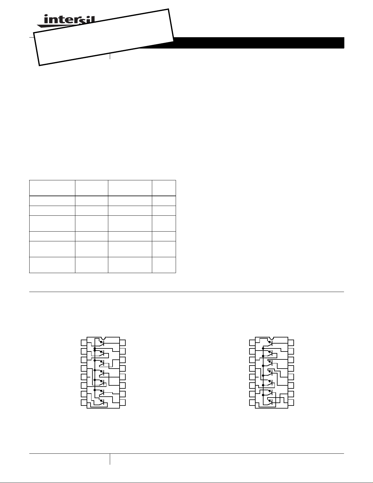
CA3081
COMMON EMITTER CONFIGURATION
SUBSTRATE
(PDIP, CERDIP, SOIC)
TOP VIEW
1
2
3
4
5
6
7
8
16
15
14
13
12
11
10
9
1
CA3082
COMMON COLLECTOR CONFIGURATION
SUBSTRATE
CAUTION: These devices are sensitive to electrostatic discharge; follow proper IC Handling Procedures.
1-888-INTE RSIL o r 321-724-7143
| Inter sil (and design) is a r egistered tr ademark of Intersi l Americas Inc.
(PDIP, SOIC)
TOP VIEW
1
2
3
4
5
6
7
8
Copyright © Intersil Americas Inc. 2002. All Rights Reserved
16
15
14
13
12
11
10
9

CA3081, CA3082
Absolute Maximum Ratings T
Collector-to-Emitter Voltage (V
Collector-to-Base Voltage (V
Collector- to-Substrate Voltage (V
Emitter-to-Base Voltage (V
Collector Current (I
Base Current (I
). . . . . . . . . . . . . . . . . . . . . . . . . . . . . . . 100mA
C
). . . . . . . . . . . . . . . . . . . . . . . . . . . . . . . . . . . 20mA
B
CEO
CBO
) . . . . . . . . . . . . . . . . . . . . . . . . . 5V
EBO
Operating C o ndi t io ns
Temperature Range. . . . . . . . . . . . . . . . . . . . . . . . . -55oC to 125oC
CAUTION: Stress es abov e thos e lis ted in “ A bsolute Max imum R a tings” ma y cause per manen t dam age to th e de vice. This is a s tress on ly rating and ope rat ion of th e
device at these or any other conditions above those indicated in the operational sections of this specification is not implied.
=25oC Thermal Informa t ion
A
) . . . . . . . . . . . . . . . . . . . . . .16V
). . . . . . . . . . . . . . . . . . . . . . . 20V
, Note 1) . . . . . . . . . . . . . 20V
CIO
Thermal Resistance (Typical, Note 2) θ
CERDIP Package. . . . . . . . . . . . . . . . . 115 45
PDIP Package . . . . . . . . . . . . . . . . . . . 100 N/A
SOIC Package . . . . . . . . . . . . . . . . . . . 190 N/A
Maximum Power Dissipation (Any One Transistor). . . . . . . 500mW
Maximum Junction Temper ature (Ceramic Package). . . . . . . . .175
Maximum Junction Temperature (Plastic Package) . . . . . . . .150
Maximum Storage Temperature Range . . . . . . . . . -65
Maximum Lead Temperature (Soldering 10s) . . . . . . . . . . . . 300
(SOIC - Lead Tips Only)
(oC/W) θJC (oC/W)
JA
o
C to 150oC
o
o
o
NOTES:
1. The collector of each transistor of the CA3081 and CA3082 is isolated from the substrate by an integral diode. The substrate must be connected
to a voltage which is more negative than any collector voltage in order to maintain isolation between transistors and provide normal transistor
action. To avoid undesired coupling between transistors, the substrate terminal (5) should be maintained at either DC or signal (AC) ground. A
suitable bypass capacitor can be used to establish a signal ground.
2. θ
is measured with t he component mounted on an evaluation PC board in free ai r.
JA
Electrical Specifications For Equipment Design at T
= 25oC
A
PARAMETER SYMBOL TEST CONDITIONS MIN TYP MAX UNITS
Collector-to-Base Breakdown Voltage V
Collec tor-to- Substrat e B rea k do w n Voltage V
Collector-to-Emitter Breakdown Voltage V
Emitter -to-Base Breakdown Voltage V
(BR)CBOIC
(BR)CIOIC
(BR)CEOIC
(BR)EBOIC
DC Forward Current Transfer Ratio h
Base-to-Emitter Saturation Voltage (Figure 4) V
Collector-to-Emitter Saturation Voltage V
FE
BESATIC
CESAT
= 500µA, IE = 0 20 60 - V
= 500µA, IB = 0 20 60 - V
= 1mA, IB = 0 16 24 - V
= 500µA5.06.9-V
VCE = 0.5V, IC = 30mA 30 68 - -
= 0.8V, IC = 50mA 40 70 - -
V
CE
= 30mA, IB = 1mA - 0.87 1.2 V
CA3081, CA3082 IC = 30mA, IB = 1mA - 0.27 0.5 V
CA3081 (Figure 5) I
CA3082 (Figure 5) I
Collector Cutoff Current I
Collector Cutoff Current I
CEO
CBO
= 50mA, IB = 5mA - 0.4 0.7 V
C
= 50mA, IB = 5mA - 0.4 0.8 V
C
VCE = 10V, IB = 0 - - 1 0 µA
VCB = 10V, IE = 0 - - 1.0 µA
C
C
C
Typical Read - Out Driver Applications
V+
1 SEGMENT OF INCANDESCENT DISPLAY
(DR2000 SERIES OR EQUIVALENT)
FROM
DECODER
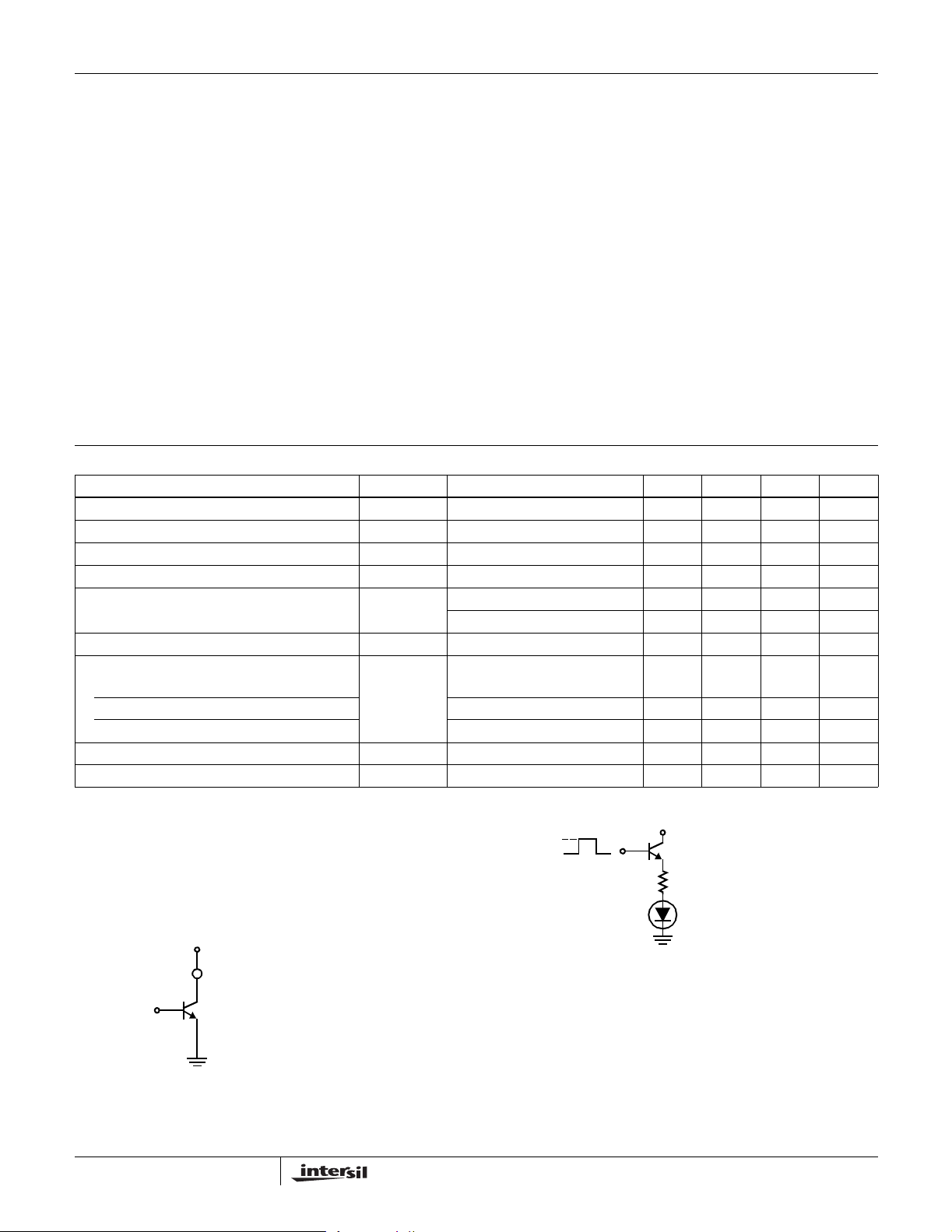
FIGURE 1. SCHEMATIC DIAGRAM SHOWING ONE
1/7 CA3081
(COMMON EMITTER)
TRANSISTOR OF THE CA3081 DRIVING ONE
SEGMENT OF AN INCANDESCENT DISPLAY
2
V
0V
P
V+
1/7 CA3082
(COMMON COLLECTOR)
R (NOTE)
LIGHT EMITTING DIODE (LED)
40736R
NOTE: The Resistance for R is determined by the relationship:
V
PVBEVF
R
----- ----------- ------------ ----------- ----------- ---- -=
ILED()
R0forV
Where: V
PVBEVF
= Input Pulse Voltage
P
V
= Forward Voltage Drop Across th e Diode
F
LED()––
LED()+==
FIGURE 2. SCHEMATIC DIAGRAM SHOWING ONE
TRANSISTOR OF THE CA3082 DRIVING A LIGHT
EMITTING DIODE (LED)
 Loading...