

CA3078, CA3078A
Data Sheet December 1998 File Number 535.5
2MHz, Micropower Operational Amplifier
The CA3078 and CA3078A are high gain monolithic
operational amplifiers which can deliver milliamperes of
current yetonlyconsumemicrowattsofstandbypower.Their
operating points are externally adjustable and frequency
compensation may be accomplished with one external
capacitor. The CA3078 and CA3078A provide the designer
with the opportunity to tailor the frequency response and
improve the slew rate without sacrificing power. Operation
with a single 1.5V battery is a practical reality with these
devices.
The CA3078A is a premium device having a supply voltage
range of V± = 0.75V to V± = 15V.The CA3078 has the same
lower supply voltage limit but the upper limit is V+ = +6V and
V- = -6V.
Ordering Information
PART NUMBER
(BRAND)
CA3078AE -55 to 125 8 Ld PDIP E8.3
CA3078AM
(3078A)
CA3078AM96
(3078A)
CA3078AT -55 to 125 8 Pin Metal Can T8.C
CA3078E 0 to 70 8 Ld PDIP E8.3
CA3078M
(3078)
CA3078T 0 to 70 8 Pin Metal Can T8.C
TEMP.
PKG.
RANGE (oC) PACKAGE
-55 to 125 8 Ld SOIC M8.15
-55 to 125 8 Ld SOIC Tape and Reel M8.15
0 to 70 8 Ld SOIC M8.15
NO.
Features
• Low Standby Power . . . . . . . . . . . . . . . As Low As 700nW
• Wide Supply Voltage Range. . . . . . . . . . . ±0.75V to ±15V
• High Peak Output Current . . . . . . . . . . . . . . . 6.5mA (Min)
• Adjustable Quiescent Current
• Output Short Circuit Protection
Applications
• Portable Electronics • Intrusion Alarms
• Telemetry • Instrumentation
• Medical Electronics
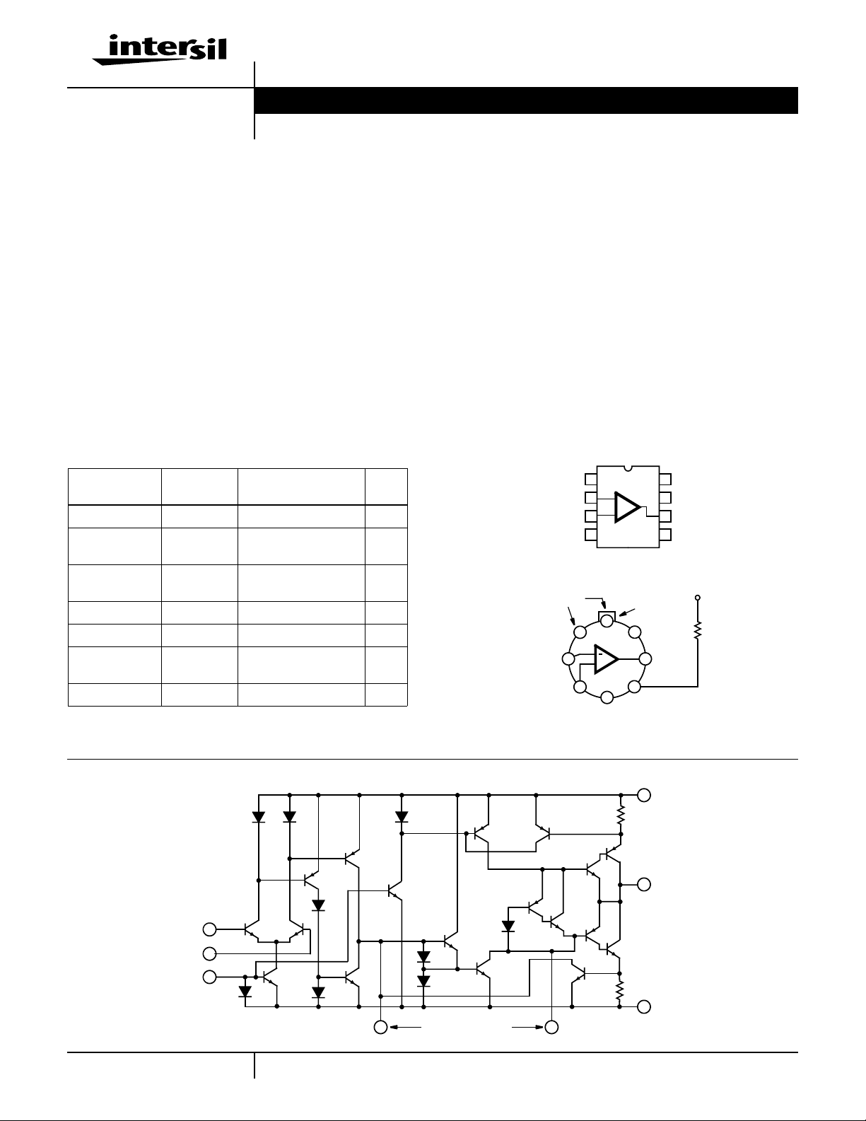
Pinouts
CA3078 (PDIP, SOIC)
TOP VIEW
COMP
1
INPUT
2
3
4
V-
INV. INPUT
NON-INV.
CA3078 (METAL CAN)
TOP VIEW
COMP
8
1
INV.
2
INPUT
NON-INV.
INPUT
+
3
4
V-
NOTE: Case Voltage = Floating
-
+
TAB
7
5
V+
6
OUTPUT
BIAS
8
COMP
7
V+
OUTPUT
6
5
BIAS
V+
R
SET
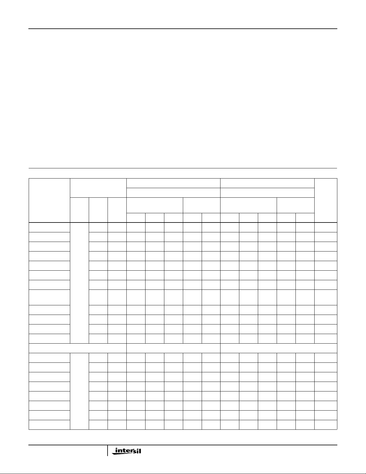
Schematic Diagram
NONINVERTING
3
INVERTING
2
BIAS
5
7
D
2
Q
D
1
1
D
3
Q
6
Q
4
D
9
Q
3
1
Q
2
D
4
Q
5
CAUTION: These devices are sensitive to electrostatic discharge; follow proper IC Handling Procedures.
D
5
Q
7
Q
8
D
6
D
7
1
COMPENSATION
1-888-INTERSIL or 321-724-7143
Q
Q
12
10
Q
11
D
8
Q
9
8
50Ω
Q
13
Q
14
50Ω
V+
Q
18
Q
OUTPUT
16
6
Q
15
Q
17
V-
4
| Copyright © Intersil Corporation 1999
CA3078, CA3078A
Absolute Maximum Ratings Thermal Information
Supply Voltage (Between V+ and V- Terminal)
CA3078 . . . . . . . . . . . . . . . . . . . . . . . . . . . . . . . . . . . . . . . . . .14V
CA3078A . . . . . . . . . . . . . . . . . . . . . . . . . . . . . . . . . . . . . . . . .36V
Differential Input Voltage . . . . . . . . . . . . . . . . . . . . . . . . . . . . . . . .6V
Input Voltage . . . . . . . . . . . . . . . . . . . . . . . . . . . . . . . . . . . . V+ to V-
Input Current . . . . . . . . . . . . . . . . . . . . . . . . . . . . . . . . . . . . . .0.1mA
Output Short Circuit Duration (Note 1). . . . . . . . . . . . . No Limitation
Operating Conditions
Temperature Range
CA3078 . . . . . . . . . . . . . . . . . . . . . . . . . . . . . . . . . . 0oC to 70oC
CA3078A . . . . . . . . . . . . . . . . . . . . . . . . . . . . . . . -55oC to 125oC
CAUTION: Stresses above those listed in “Absolute Maximum Ratings” may cause permanent damage to the device. This is a stress only rating and operation of the
device at these or any other conditions above those indicated in the operational sections of this specification is not implied.
NOTES:
1. Short circuit may be applied to ground or to either supply.
2. θJA is measured with the component mounted on an evaluation PC board in free air.
Electrical Specifications For Equipment Design
CA3078 LIMITS CA3078A LIMITS
TEST CONDITIONS
PARAMETER
V
IO
I
IO
I
IB
A
OL
I
Q
P
D
V
OM
V
ICR
V+
and V-
±6V ≤10 - - 1.3 4.5 - 5 - 0.70 3.5 - 4.5 mV
R
(kΩ)
R
S
(kΩ)
L
MIN TYP MAX MIN MAX MIN TYP MAX MIN MAX
- - - 6 32 - 40 - 0.50 2.5 - 5.0 nA
- - - 60 170 - 200 - 7 12 - 50 nA
- ≥10 88 92 - 86 - 92 100 - 90 - dB
- - - 100 130 - 150 - 20 25 - 45 µA
- - - 1200 1560 - 1800 - 240 300 - 540 µW
- ≥10 ±5.1 ±5.3 - ±5-±5.1 ±5.3 - ±5- V
≤10 - - -5.5 to
CMRR ≤10 - 80 110 - - - 80 115 - - - dB
IOM+ or IOM- - - - 12 - 6.5 30 - 12 - 6.5 30 mA
∆VIO/∆V+ ≤10 - 76 93 - - - 76 105 - - - µV/V
∆VIO/∆V- ≤10 - 76 93 - - - 76 105 - - - µV/V
V
IO
A
OL
I
Q
P
D
V
OM
±15V ≤10 - - - - - - - 1.4 3.5 - 4.5 mV
- ≥10 - - - - - 92 100 - 88 - dB
--------2030-50µA
- - - - - - - - 600 750 - 1350 µW
- ≥10-----±13.7 ±14.1 - ±13.5 - V
CMRR ≤10 - - - - - - 80 106 - - - dB
I
IB
I
IO
--------714-55nA
- - - - - - - - 0.50 2.7 - 5.5 nA
R
TA = 25oC
+5.8
= 1MΩ R
SET
- -5 to
Thermal Resistance (Typical, Note 2) θJA (oC/W) θJC (oC/W)
PDIP Package . . . . . . . . . . . . . . . . . . . 130 N/A
SOIC Package . . . . . . . . . . . . . . . . . . . 165 N/A
Metal Can Package . . . . . . . . . . . . . . . 175 100
Maximum Junction Temperature (Metal Can Package). . . . . . . .175oC
Maximum Junction Temperature (Plastic Package) . . . . . . . .150oC
Maximum Storage Temperature Range. . . . . . . . . . -65oC to 150oC
Maximum Lead Temperature (Soldering 10s) . . . . . . . . . . . . 300oC
(SOIC - Lead Tips Only)
= 5.1MΩ
SET
TA = 0oC to
70oCT
= 25oC
A
TA = -55oC to
125oC
UNITS
+5
- - -5.5 to
+5.8
- -5 to
R
= 13MΩ
SET
-V
+5
2
CA3078, CA3078A
Electrical Specifications T
= 25oC, Typical Values Intended Only for Design Guidance
A
CA3078 CA3078A
PARAMETER
V
IO
I
IO
I
IB
A
OL
I
Q
P
D
V
OP-P
V
ICR
V+ = +1.3V,
V- = -1.3V
R
= 2MΩ
SET
1.3 1.5 0.7 0.9 mV
1.7 0.5 0.3 0.054 nA
9 1.3 3.7 0.45 nA
80 60 84 65 dB
10 1 10 1 µA
26 1.5 26 1.5 µW
1.4 0.3 1.4 0.3 V
-0.8 to +1.1 -0.2 to +0.5 -0.8 to +1.1 -0.2 to +0.5 V
V+ = +0.75V,
V- = -0.75V
R
= 10MΩ
SET
V+ = +1.3V,
V- = -1.3V
R
= 2MΩ
SET
V+ = +0.75V,
V- = -0.75V
R
= 10MΩ
SET
CMRR 100 90 100 90 dB
IOM± 12 0.5 12 0.5 mA
∆VIO/∆V± 20 50 20 50 µV/V
Electrical Specifications T
= 25oC and V
A
SUPPLY
= ±6V, Typical Values Intended Only for Design Guidance
CA3078 CA3078A
PARAMETER TEST CONDITIONS
∆VIO/∆T
∆IIO/∆T
RS≤10kΩ 656µV/oC
A
RS≤10kΩ 70 6.3 70 pA/oC
A
= 1MΩ R
SET
= 5.1MΩ R
SET
SET
= 1MΩ
GBWP AV = 100, C1 = 10pF 2 0.3 2 MHz
SR See Figures 23, 24 0.04 0.027 0.04 V/µs
1.5 0.5 1.5 V/µs
t
R
R
I
R
O
10% to 90% Rise Time 2.5 3 2.5 µs
- 0.87 7.4 1.7 MΩ
- 0.8 1 0.8 kΩ
eN(10Hz) RS = 0 25 40 - nV/√Hz
iN(10Hz) RS = 1MΩ 1 0.25 - pA/√Hz
UNITS
UNITSR
3
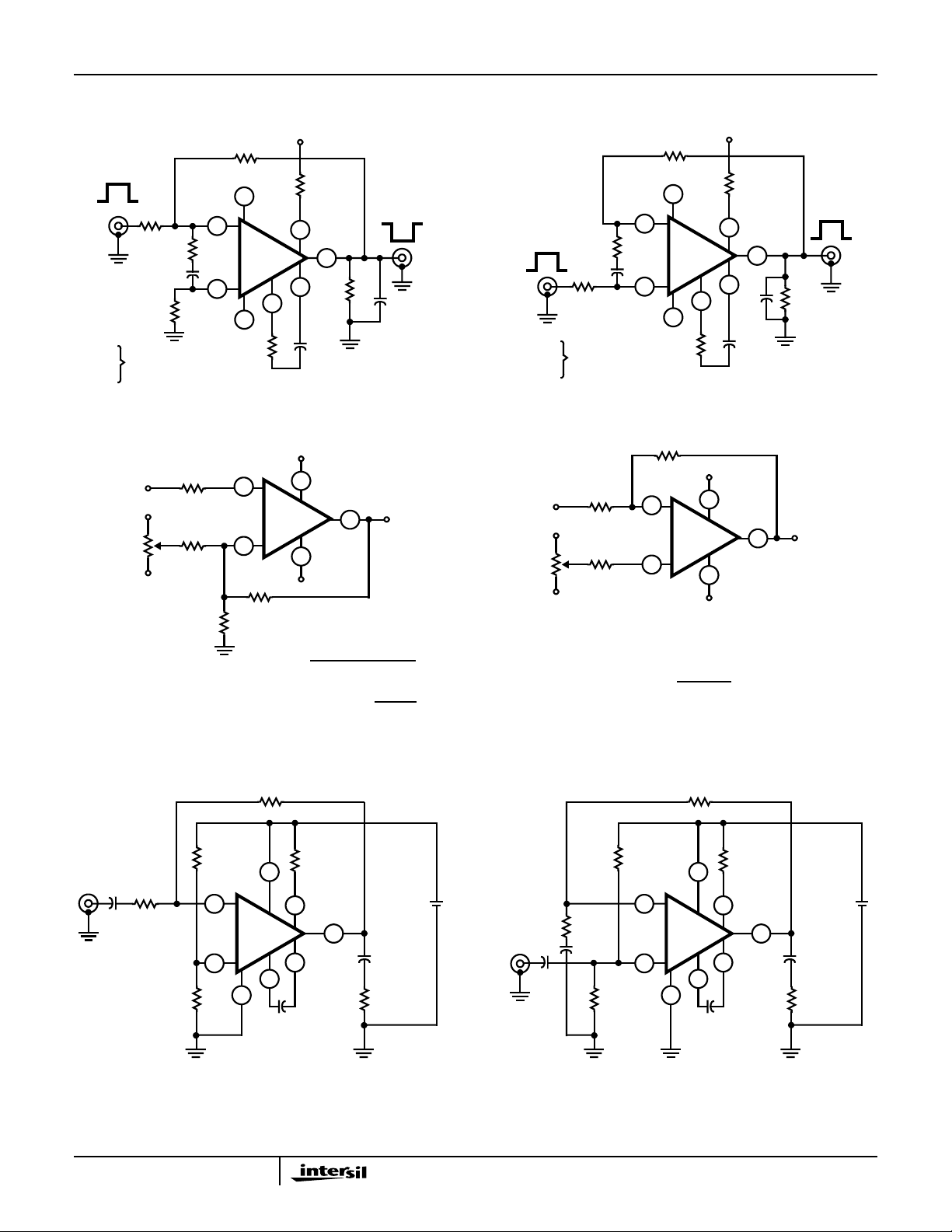
Test Circuits
100kΩ
V+
CA3078, CA3078A
V+
100kΩ
0V
V
IN
R2 - C
R
1
2
100kΩ
R
C
51kΩ
OPTIONAL
COMP.
V+
7
2
-
3
CA3078
CA3078A
+
4
V-
R
1
2
2
R
SET
5
6
8
1
10kΩ
C
1
C
L
FIGURE1. TRANSIENT RESPONSE ANDSLEWRATE,UNITY
GAIN (INVERTING) TEST CIRCUIT
NON-INVERTING
INPUT
V+
1M
V-
R
I
R
B
3
2
R
R
I
V+
7
+
CA3078
CA3078A
-
F
4
V-
6
OUTPUT
Value of RB required to have a
null adjustment range of ±7.5mV
R
B
assuming RB > >
RI RF V+
≈
(RI + RF) 7.5 x 10
RI R
RI + R
-3
F
F
V
0V
OUT
0V
V
IN
R2 - C
R
1
2
R
2
C
2
100kΩ
OPTIONAL
COMP.
2
3
V+
7
-
CA3078
CA3078A
+
4
V-
R
1
R
SET
5
6
8
C
1
C
10kΩ
L
1
FIGURE 2. SLEW RATE,UNITY GAIN (NON-INVERTING)
TEST CIRCUIT
INVERTING
R
INPUT
V+
1M
V-
F
R
I
R
B
2
3
7
-
CA3078
CA3078A
+
4
V+
V-
OUTPUT
6
Value of RB required to have a
null adjustment range of ±7.5mV
RI V+
R
≈
B
assuming RB > > R
7.5 x 10
-3
I
V
0V
OUT
FIGURE 3. OFFSET VOLTAGE NULL CIRCUITS
5.1MΩ
R
5
8
SET
30MΩ
=
6
1.5V
“AA” CELL
+
5µF
R
L
10MΩ
+
-
510kΩ
V
P-P
1µF
1µF
10MΩ
10MΩ
V
P-P
510kΩ
1µF
10MΩ
2
3
7
-
CA3078
CA3078A
+
1
4
7pF
2
3
5.1MΩ
7
-
CA3078
CA3078A
+
1
4
7pF
5
8
R
SET
30MΩ
=
6
FIGURE 4. INVERTING 20dB AMPLIFIER CIRCUIT FIGURE 5. NON-INVERTING 20dB AMPLIFIER CIRCUIT
4
1.5V
“AA” CELL
+
5µF
R
L
+
-

TABLE 1. UNITY GAIN SLEW RATE vs COMPENSATION - CA3078 AND CA3078A
V
Ambient Temperature (TA) = 25oC
CA3078 - IQ = 100µA
Single Capacitor 0 750
Resistor and Capacitor 3.5 350
Input
CA3078A - IQ = 20µA
Single Capacitor 0 300
Resistor and Capacitor 14 100
Input
= ±6V, Output Voltage (VO)=±5V, Load Resistance (RL) = 10kΩ, Transient Response: 10% overshoot for an output voltage of 100mV,
SUPPLY
R
COMPENSATION
TECHNIQUE
1
kΩ pF kΩµFV/µskΩ pF kΩµFV/µs
∞
∞
CA3078, CA3078A
UNITY GAIN (INVERTING)
FIGURE 1
C
1
0 0.25 0.306 0.67
0 0.644 0.156 0.29
R
2
∞
∞
∞
∞
C
SLEW RA TE R
2
0 0.0085 0 1500
0 0.04 5.3 500
0 0.0095 0 800
0 0.027 34 125
UNITY GAIN (NON-INVERTING)
FIGURE 2
1
C
1
R
∞
∞
∞
0 0.311 0.45 0.67
∞
∞
∞
0 0.77 0.4 0.4
C
2
SLEW RA TE
2
0 0.0095
0 0.024
0 0.003
0 0.02
Application Information
Compensation Techniques
The CA3078A and CA3078 can be phase compensated with
one or two external components depending upon the closed
loop gain, power consumption, and speed desired. The
recommended compensation is a resistor in series with a
capacitor connected from Terminal 1 to Terminal 8. Values of
the resistor and capacitor required for compensation as a
function of closed loop gain are shown in Figures 25 and 26.
These curves represent the compensation necessary at
quiescent currents of 100µA and 20µA, respectively, for a
transient response with 10% overshoot. Figures 23 and 24
show the slew rates that can be obtained with the two different
compensation techniques. Higher speeds can be achieved
Typical Performance Curves
VS = ±6
T
= 25oC
A
≤ 10kΩ
R
S
3.0
2.4
1.8
1.2
0.6
INPUT OFFSET VOLTAGE (mV)
0
1 10 100
TOTAL QUIESCENT CURRENT (µA)
CA3078
CA3078A
1000
with input compensation, but this increases noise output.
Compensation can also be accomplished with a single
capacitor connectedfrom Terminal1 to Terminal8, with speed
being sacrificed for simplicity. Tab le 1 gives an indication of
slew rates that can be obtained with various compensation
techniques at quiescent currents of 100µA and 20µA.
Single Supply Operation
The CA3078A and CA3078 can operate from a single supply
with a minimum total supply voltage of 1.5V. Figures 4 and 5
show the CA3078A or CA3078 in inverting and non-inverting
20dB amplifier configurations utilizing a 1.5V type “AA” cell
for a supply. The total consumption for either circuit is
approximately 675nW. The output voltage swing in this
configuration is 300mV
= ±6
V
S
TA = 25oC
10
CA3078
1
0.1
INPUT OFFSET CURRENT (nA)
0.01
1 10 1000
TOTAL QUIESCENT CURRENT (µA)
with a 20kΩ load.
P-P
CA3078A
100
10000
FIGURE 6. INPUT OFFSET VOLTAGEvs TOTAL QUIESCENT
CURRENT
5
FIGURE 7. INPUTOFFSET CURRENT vs TOTAL QUIESCENT
CURRENT

Typical Performance Curves (Continued)
CA3078, CA3078A
VS = ±6
= 25oC
T
A
100
10
INPUT BIAS CURRENT (nA)
0.1
CA3078
CA3078A
1
1 10 1000
TOTAL QUIESCENT CURRENT (µA)
10000100
FIGURE 8. INPUT BIAS CURRENT vs TOTALQUIESCENT
CURRENT
1000
= ±15
V
100
10
1
0.1
BIAS SETTING RESISTANCE (MΩ)
0.01
1000 100 10 1 0.1 0.01 0.001
S
+6
-6
+3
-3
+1
-1
TA = 25oC
R
CONNECTED BETWEEN
SET
TERMINAL 5 AND V+
TOTAL QUIESCENT CURRENT (µA)
TA = 25oC
CA3078A
126
RL = 1MΩ
108
90
72
54
36
18
OPEN LOOP VOLTAGE GAIN (dB)
0
1 10 100
10kΩ
2kΩ
TOTAL QUIESCENT CURRENT (µA)
FIGURE 9. OPEN LOOP VOLTAGEGAIN vs TOTAL
QUIESCENT CURRENT
100
VS = ±6 TO VS = ±15
T
= 25oC
A
10
1
MAXIMUM OUTPUT CURRENT (mA)
0.1
1 10 100
TOTAL QUIESCENT CURRENT (µA)
1000
CA3078
126
108
90
72
54
36
18
0
1000
FIGURE 10. BIAS SETTING RESISTANCEvs TOTAL
QUIESCENT CURRENT
VS = ±1.3V
TA = 25oC
1.5
1.0
0.5
OUTPUT VOLTAGE SWING (V)
0
0 0.5 1.0 1.5 2.0
TOTAL QUIESCENT CURRENT (µA)
RL = 50kΩ
10kΩ
5kΩ
2kΩ
1kΩ
500Ω
FIGURE12. OUTPUT VOLTAGE SWING vs TOTAL QUIESCENT
CURRENT
6
FIGURE 11. MAXIMUM OUTPUT CURRENT vs TOTAL
QUIESCENT CURRENT
VS = ±6
= 100µA
I
120
Q
100
80
100
300
60
1000
40
20
0
= 10kΩ, TA = 25oC
R
L
OPEN LOOP VOLTAGE GAIN (dB)
C1- BETWEEN TERMINALS 1 AND 8
-20
0.1 1 10
1
FREQUENCY (Hz)
10210310410510
C1 = 0pF
C
= 10pF
1
C
= 30pF
1
0
100
φ
200
300
400
6
FIGURE 13. OPEN LOOP VOLTAGE GAIN vs FREQUENCY
PHASE ANGLE (DEGREES)

Typical Performance Curves (Continued)
CA3078, CA3078A
100
IQ = 20µA
TA = 25oC
10
1
0.1
+0.1
-0.1
-0.1
-1
PEAK OUTPUT VOLTAGE (V), COMMON MODE V OLTAGE RANGE (V)
V
ICR
V
OM
+100+10+1
-1 -10 -100
SUPPLY VOLTS (V+, V-)
-V
ICR
-V
OM
VS = ±6
120
= 20µA
I
Q
100
80
60
100
300
40
1000
20
OPEN LOOP VOLTAGE GAIN (dB)
= 10kΩ
R
0
L
TA = 25oC
- BETWEEN TERMINALS 1 AND 8
C
1
-20
0.1 1 10
1
10210310410510
FREQUENCY (Hz)
C1 = 0pF
C
C
= 10pF
1
= 30pF
1
φ
0
100
200
300
400
6
FIGURE 15. OPEN LOOP VOLTAGE GAIN vs FREQUENCY
1.75
VS = ±6
1.50
CA3078
I
= 100µA
1.25
1.00
0.75
Q
CA3078A
I
= 20µA
Q
PHASE ANGLE (DEGREES)
-10
FIGURE 14. OUTPUT AND COMMON MODE VOLTAGE vs
SUPPLY VOLTAGE
VS = ±6
2.5
2.0
1.5
CA3078A
I
1.0
0.5
INPUT OFFSET CURRENT (nA) - CA3078AT
0
= 20µA
Q
TEMPERATURE (
CA3078
I
= 100µA
Q
o
C)
1251007550250-25-50-75
0.50
INPUT OFFSET VOLTAGE (mV)
0.25
0
FIGURE 16. INPUT OFFSET VOLTAGE vs TEMPERATURE
VS = ±6
15.0
10
8
6
4
2
INPUT OFFSET CURRENT (nA) - CA3078T
0
12.5
10.0
7.5
5.0
2.5
INPUT BIAS CURRENT (nA) - CA3078AT
00
TEMPERATURE (oC)
CA3078A
I
= 20µA
Q
CA3078
I
= 100µA
Q
TEMPERATURE (
125
1007550250-25-50-75
100
75
50
25
INPUT BIAS CURRENT (nA) - CA3078T
o
C)
1251007550250-25-50-75
FIGURE 17. INPUT OFFSET CURRENT vs TEMPERATURE FIGURE 18. INPUT BIAS CURRENT vs TEMPERATURE
7

Typical Performance Curves (Continued)
CA3078, CA3078A
VS = ±6
110
105
100
95
90
85
OPEN LOOP VOLTAGE GAIN (dB)
80
CA3078A
I
= 20µA
Q
CA3078
I
= 100µA
Q
TEMPERATURE (
125
1007550250-25-50-75
o
C)
VS = ±6
50
40
30
20
10
0
TOTAL QUIESCENT CURRENT (µA) - CA3078AT
TEMPERATURE (
CA3078
CA3078A
o
C)
1251007550250-25-50-75
200
150
100
50
0
TOTAL QUIESCENT CURRENT (µA) - CA3078T
FIGURE 19. OPEN LOOP VOLTAGE GAIN vs TEMPERATURE FIGURE 20. TOTAL QUIESCENT CURRENT vs TEMPERATURE
100
10
VS = ±6
= 25oC
T
A
CA3078AT
IQ = 20µA
IQ = 100µA
0.1
1
IQ = 20µA
IQ = 100µA
VS = ±6
T
= 25oC
A
CA3078AT
EQUIVALENT INPUT NOISE VOLT A GE (nV/√Hz)
0
1
10
2
10
FREQUENCY (Hz)
3
10
4
10
FIGURE 21. EQUIVALENT INPUT NOISE VOLTAGE vs
FREQUENCY
EQUIVALENT INPUT NOISE CURRENT (pA/√Hz)
5
10
0.01
1
10
2
10
3
10
FREQUENCY (Hz)
4
10
5
10
FIGURE 22. EQUIVALENT INPUT NOISE CURRENT vs
FREQUENCY
8

Typical Performance Curves (Continued)
RESISTOR-CAPACITOR
1.5
1.25
0.75
0.5
SLEW RATE (V/µs)
0.25
COMPENSATION
- C1 BETWEEN
(R
1
TERMINALS 1 AND 8)
1
CAP A CIT OR
COMPENSATION
(BETWEEN
TERMINALS 1 AND 8)
CA3078, CA3078A
0.6
0.5
0.4
0.3
0.2
SLEW RATE (V/µs)
0.1
RESISTOR-CAPACITOR
COMPENSATION
- C1 BETWEEN
(R
1
TERMINALS 1 AND 8)
CAP A CIT OR
COMPENSATION
(BETWEEN
TERMINALS 1 AND 8)
0
CLOSED LOOP NON-INVERTING VOLTAGE GAIN (dB)
CLOSED LOOP INVERTING VOLTAGE GAIN (dB)
6050403020100
908070
90807060504029.719.16
Supply Volts: V+ = +6, V- = -6
Quiescent Current (IQ) = 100µA
Ambient Temperature (TA) = 25oC
Load Impedance: RL = 10kΩ, CL = 100pF
Feedback Resistance (RF) = 0.1MΩ
Output Voltage (V
OP-P
) = 10V
R1determined for transient response with 10% overshoot on a
100mV output signal (R1 x C1 = 2.5 x 10⁻⁶)
FIGURE 23. SLEW RATE vs CLOSED LOOP GAIN FOR
IQ = 100mA - CA3078
1000
100
CAP A CIT OR
COMPENSATION
(BETWEEN
TERMINALS 1 AND 8)
RESISTOR-CAPACITOR
COMPENSATION
- C1 BETWEEN
(R
1
TERMINALS 1 AND 8)
0
CLOSED LOOP NON-INVERTING VOLTAGE GAIN (dB)
CLOSED LOOP INVERTING VOLTAGE GAIN (dB)
6050403020100
908070
90807060504029.719.16
Supply Volts: V+ = +6, V- = -6
Quiescent Current (IQ) = 20µA
Ambient Temperature (TA) = 25oC
Load Impedance: RL = 10kΩ, CL = 100pF
Feedback Resistance (RF) = 0.1MΩ
Output Voltage (V
OP-P
) = 10V
R1determined for transient response with 10% overshoot on a
100mV output signal (R1 x C1 = 2 x 10⁻⁶)
FIGURE 24. SLEW RATE vs CLOSED LOOP GAIN FOR
IQ = 20mA - CA3078A
1000
100
CAP A CIT OR
COMPENSATION
(BETWEEN
TERMINALS 1 AND 8)
RESISTOR-CAPACITOR
COMPENSATION
- C1 BETWEEN
(R
1
TERMINALS 1 AND 8)
10
1
PHASE COMPENSATION CAPACITOR (pF)
CLOSED LOOP NON-INVERTING VOLTAGE GAIN (dB)
6050403020100
CLOSED LOOP INVERTING VOLTAGE GAIN (dB)
908070
90807060504029.719.16
Supply Volts: V+ = +6, V- = -6
Quiescent Current (IQ) = 100µA
Ambient Temperature (TA) = 25oC
Load Impedance: RL = 10kΩ, CL = 100pF
Feedback Resistance (RF) = 0.1MΩ
Output Voltage (V
OP-P
) = 100mV
R1determined for transient response with 10% overshoot on a
100mV output signal (R1 x C1 = 2.5 x 10⁻⁶)
FIGURE 25. PHASECOMPENSATIONCAPACITANCE vs
CLOSED LOOP GAIN - CA3078
9
10
1
PHASE COMPENSATION CAPACITOR (pF)
CLOSED LOOP NON-INVERTING VOLTAGE GAIN (dB)
6050403020100
CLOSED LOOP INVERTING VOLTAGE GAIN (dB)
908070
90807060504029.719.16
Supply Volts: V+ = +6, V- = -6
Quiescent Current (IQ) = 20µA
Ambient Temperature (TA) = 25oC
Load Impedance: RL = 10kΩ, CL = 100pF
Feedback Resistance (RF) = 0.1MΩ
Output Voltage (V
OP-P
) = 100mV
R1determined for transient response with 10% overshoot on a
100mV output signal (R1 x C1 = 2 x 10⁻⁶)
FIGURE 26. PHASECOMPENSATIONCAPACITANCE vs
CLOSED LOOP GAIN - CA3078A

Dual-In-Line Plastic Packages (PDIP)
CA3078, CA3078A
N
D1
-C-
E1
-B-
A1
A2
A
L
e
C
S
INDEX
AREA
BASE
PLANE
SEATING
PLANE
D1
B1
1 2 3 N/2
-AD
e
B
0.010 (0.25) C AMB
NOTES:
1. Controlling Dimensions: INCH. In case of conflict between
English and Metric dimensions, the inch dimensions control.
2. Dimensioning and tolerancing per ANSI Y14.5M-1982.
3. Symbols are defined in the “MO Series Symbol List” in Section
2.2 of Publication No. 95.
4. Dimensions A, A1 and L are measured with the package seated
in JEDEC seating plane gauge GS-3.
5. D, D1, and E1 dimensions do not include mold flash or protrusions. Mold flash or protrusions shall not exceed 0.010 inch
(0.25mm).
6. E and are measured with the leads constrained to be per-
e
pendicular to datum .
A
-C-
7. eB and eC are measured at the lead tips with the leads unconstrained. eC must be zero or greater.
8. B1 maximum dimensions do not include dambar protrusions.
Dambar protrusions shall not exceed 0.010 inch (0.25mm).
9. N is the maximum number of terminal positions.
10. Corner leads (1, N, N/2 and N/2 + 1) for E8.3, E16.3, E18.3,
E28.3, E42.6 will have a B1 dimension of 0.030 - 0.045 inch
(0.76 - 1.14mm).
E8.3 (JEDEC MS-001-BA ISSUE D)
8 LEAD DUAL-IN-LINE PLASTIC PACKAGE
INCHES MILLIMETERS
SYMBOL
A - 0.210 - 5.33 4
E
A1 0.015 - 0.39 - 4
A2 0.115 0.195 2.93 4.95 -
B 0.014 0.022 0.356 0.558 -
C
L
e
A
C
e
B
B1 0.045 0.070 1.15 1.77 8, 10
C 0.008 0.014 0.204 0.355 D 0.355 0.400 9.01 10.16 5
D1 0.005 - 0.13 - 5
E 0.300 0.325 7.62 8.25 6
E1 0.240 0.280 6.10 7.11 5
e 0.100 BSC 2.54 BSC -
e
A
e
B
0.300 BSC 7.62 BSC 6
- 0.430 - 10.92 7
L 0.115 0.150 2.93 3.81 4
N8 89
NOTESMIN MAX MIN MAX
Rev. 0 12/93
10

CA3078, CA3078A
Small Outline Plastic Packages (SOIC)
N
INDEX
AREA
123
-A-
0.25(0.010) B
H
E
-B-
SEATING PLANE
D
A
-C-
M
L
h x 45
M
o
α
e
B
0.25(0.010) C AMB
M
NOTES:
11. Symbols are defined in the “MO Series Symbol List” in Section 2.2 of
Publication Number 95.
12. Dimensioning and tolerancing per ANSI Y14.5M-1982.
13. Dimension “D” does not include mold flash, protrusions or gate burrs.
Mold flash, protrusion and gate burrs shall not exceed 0.15mm(0.006
inch) per side.
14. Dimension “E” does not include interlead flash or protrusions. Interlead flash and protrusions shall not exceed 0.25mm (0.010 inch) per
side.
15. The chamfer on the body is optional. If it is not present, a visual index
feature must be located within the crosshatched area.
16. “L” is the length of terminal for soldering to a substrate.
17. “N” is the number of terminal positions.
18. Terminal numbers are shown for reference only.
19. The lead width “B”, as measured 0.36mm (0.014 inch) or greater
above the seating plane, shall not exceed a maximum value of
0.61mm (0.024 inch).
20. Controlling dimension: MILLIMETER. Converted inch dimensions
are not necessarily exact.
A1
0.10(0.004)
S
C
M8.15 (JEDEC MS-012-AA ISSUE C)
8 LEAD NARROW BODY SMALL OUTLINE PLASTIC
PACKAGE
INCHES MILLIMETERS
SYMBOL
A 0.0532 0.0688 1.35 1.75 -
A1 0.0040 0.0098 0.10 0.25 -
B 0.013 0.020 0.33 0.51 9
C 0.0075 0.0098 0.19 0.25 D 0.1890 0.1968 4.80 5.00 3
E 0.1497 0.1574 3.80 4.00 4
e 0.050 BSC 1.27 BSC -
H 0.2284 0.2440 5.80 6.20 -
h 0.0099 0.0196 0.25 0.50 5
L 0.016 0.050 0.40 1.27 6
N8 87
o
α
0
o
8
o
0
o
8
Rev. 0 12/93
NOTESMIN MAX MIN MAX
-
11

Metal Can Packages (Can)
CA3078, CA3078A
REFERENCE PLANE
ØD ØD1
A
F
Q
Øb1
L
L2
L1
A
A
Øe
Øb1
Øb
BASE AND
SEATING PLANE
BASE METAL LEAD FINISH
SECTION A-A
Øb2
e1
ØD2
2
β
N
1
α
k
NOTES:
1. (All leads) Øb applies between L1 and L2. Øb1 applies between
L2 and 0.500 from the reference plane. Diameter is uncontrolled
in L1 and beyond 0.500 from the reference plane.
2. Measured from maximum diameter of the product.
3. α is the basic spacing from the centerline of the tab to terminal 1
and β is the basic spacing of each lead or lead position (N -1
places) from α, looking at the bottom of the package.
4. N is the maximum number of terminal positions.
5. Dimensioning and tolerancing per ANSI Y14.5M - 1982.
6. Controlling dimension: INCH.
T8.C MIL-STD-1835 MACY1-X8 (A1)
8 LEAD METAL CAN PACKAGE
INCHES MILLIMETERS
SYMBOL
A 0.165 0.185 4.19 4.70 -
Øb 0.016 0.019 0.41 0.48 1
k1
Øb1 0.016 0.021 0.41 0.53 1
Øb2 0.016 0.024 0.41 0.61 -
ØD 0.335 0.375 8.51 9.40 -
ØD1 0.305 0.335 7.75 8.51 -
C
L
ØD2 0.110 0.160 2.79 4.06 -
e 0.200 BSC 5.08 BSC -
e1 0.100 BSC 2.54 BSC -
F - 0.040 - 1.02 k 0.027 0.034 0.69 0.86 -
k1 0.027 0.045 0.69 1.14 2
L 0.500 0.750 12.70 19.05 1
L1 - 0.050 - 1.27 1
L2 0.250 - 6.35 - 1
Q 0.010 0.045 0.25 1.14 -
α
45o BSC 45o BSC 3
β 45o BSC 45o BSC 3
N8 84
NOTESMIN MAX MIN MAX
Rev. 0 5/18/94
All Intersil semiconductor products are manufactured, assembled and tested under ISO9000 quality systems certification.
Intersil semiconductor products are sold by description only. Intersil Corporationreserves the rightto make changes in circuit design and/or specifications at any time without notice. Accordingly, the reader is cautioned to verify that data sheets are current before placing orders. Information furnished by Intersil is believed to be accurate and
reliable. However, no responsibility is assumed by Intersil or its subsidiaries for its use; nor for any infringements of patents or other rights of third parties which may result
from its use. No license is granted by implication or otherwise under any patent or patent rights of Intersil or its subsidiaries.
For information regarding Intersil Corporation and its products, see web site www.intersil.com
Sales Office Headquarters
NORTH AMERICA
Intersil Corporation
P. O. Box 883, Mail Stop 53-204
Melbourne, FL 32902
TEL: (321) 724-7000
FAX: (321) 724-7240
12
EUROPE
Intersil SA
Mercure Center
100, Rue de la Fusee
1130 Brussels, Belgium
TEL: (32) 2.724.2111
FAX: (32) 2.724.22.05
ASIA
Intersil (Taiwan) Ltd.
7F-6, No. 101 Fu Hsing North Road
Taipei, Taiwan
Republic of China
TEL: (886) 2 2716 9310
FAX: (886) 2 2715 3029
 Loading...