Intersil Corporation CA3054 Datasheet

CA3054
Data Sheet September 1998 File Number 388.4
Dual Independent Differential Amp for
Low Power Applications from DC to
120MHz
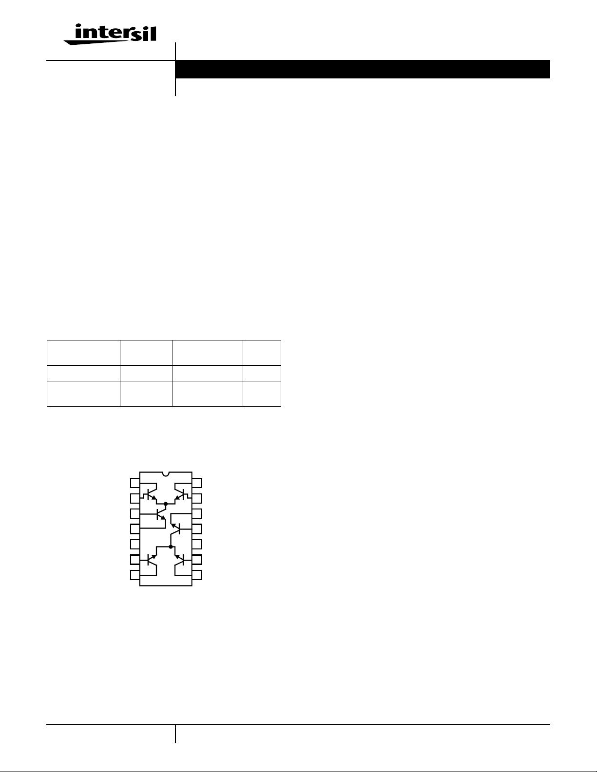
The CA3054 consists of two independent differential
amplifiers with associated constant current transistors on a
common monolithic substrate.ThesixNPNtransistorswhich
comprise the amplifiers are general purpose devices which
exhibit low 1/f noise and a value of f
in excess of 300MHz.
T
These feature make the CA3054 useful from DC to 120MHz.
Bias and load resistors have been omitted to provide
maximum application flexibility.
The monolithic construction of the CA3054 provides close
electrical and thermal matching of the amplifiers. This
feature makes these devices particularly useful in dual
channel applications where matched performance of the two
channels is required.
Ordering Information
PART NUMBER
(BRAND)
CA3054 0 to 85 14 Ld PDIP E14.3
CA3054M96
(3054)
TEMP.
RANGE (oC) PACKAGE
0 to 85 14 Ld SOIC Tape
and Reel
PKG.
NO.
M14.15
Features
• Two Differential Amplifiers on a Common Substrate
• Independently Accessible Inputs and Outputs
• Maximum Input Offset Voltage . . . . . . . . . . . . . . . . . ±5mV
o
• Temperature Range . . . . . . . . . . . . . . . . . . . 0
C to 85oC
Applications
• Dual Sense Amplifiers
• Dual Schmitt Triggers
• Multifunction Combinations
- RF/Mixer/Oscillator; Converter/IF
• IF Amplifiers (Differential and/or Cascode)
• Product Detectors
• Doubly Balanced Modulators and Demodulators
• Balanced Quadrature Detectors
• Cascade Limiters
• Synchronous Detectors
• Pairs of Balanced Mixers
• Synthesizer Mixers
Pinout
SUBSTRATE
CA3054
(PDIP, SOIC)
TOP VIEW
1
Q
2
2
3
Q
3
4
5
6
Q
5
7
• Balanced (Push-Pull) Cascode Amplifiers
14
Q
1
13
12
11
Q
4
NC
10
9
Q
6
8
1
CAUTION: These devices are sensitive to electrostatic discharge; follow proper IC Handling Procedures.
1-888-INTERSIL or 321-724-7143
| Copyright © Intersil Corporation 1999

CA3054
Absolute Maximum Ratings T
Collector-to-Emitter Voltage, V
Collector-to-Base Voltage, V
Collector-to-Substrate Voltage, V
Emitter-to-Base Voltage, V
Collector Current, IC . . . . . . . . . . . . . . . . . . . . . . . . . . . . . . . . 50mA
CEO
. . . . . . . . . . . . . . . . . . . . . . . . 20V
CBO
CIO
. . . . . . . . . . . . . . . . . . . . . . . . . . 5V
EBO
=25oC Thermal Information
A
. . . . . . . . . . . . . . . . . . . . . . 15V
Thermal Resistance (Typical, Note 2) θJA (oC/W)
PDIP Package . . . . . . . . . . . . . . . . . . . . . . . . . . . . . 130
(Note 1). . . . . . . . . . . . . . 20V
SOIC Package . . . . . . . . . . . . . . . . . . . . . . . . . . . . . 140
Maximum Junction Temperature (Die) . . . . . . . . . . . . . . . . . . . .175oC
Maximum Junction Temperature (Plastic Package) . . . . . . . .150oC
Maximum Storage Temperature Range. . . . . . . . . . -65oC to 150oC
Operating Conditions
Temperature Range. . . . . . . . . . . . . . . . . . . . . . . . . . . 0oC to 85oC
CAUTION: Stresses above those listed in “Absolute Maximum Ratings” may cause permanent damage to the device. This is a stress only rating and operation of the
device at these or any other conditions above those indicated in the operational sections of this specification is not implied.
Maximum Lead Temperature (Soldering 10s) . . . . . . . . . . . . 300oC
(SOIC - Lead Tips Only)
Maximum Power Dissipation (Any One Transistor) . . . . . . . 300mW
NOTES:
1. The collector of each transistor of the CA3054 is isolated from the substrate by an integral diode. The substrate must be connected to a voltage
which is more negative than any collector voltage in order to maintain isolation between transistors and provide for normal transistor action. The
substrate shouldbe maintained at signal (AC) groundby means of a suitable groundingcapacitor, to avoidundesired coupling between transistors.
2. θJA is measured with the component mounted on an evaluation PC board in free air.
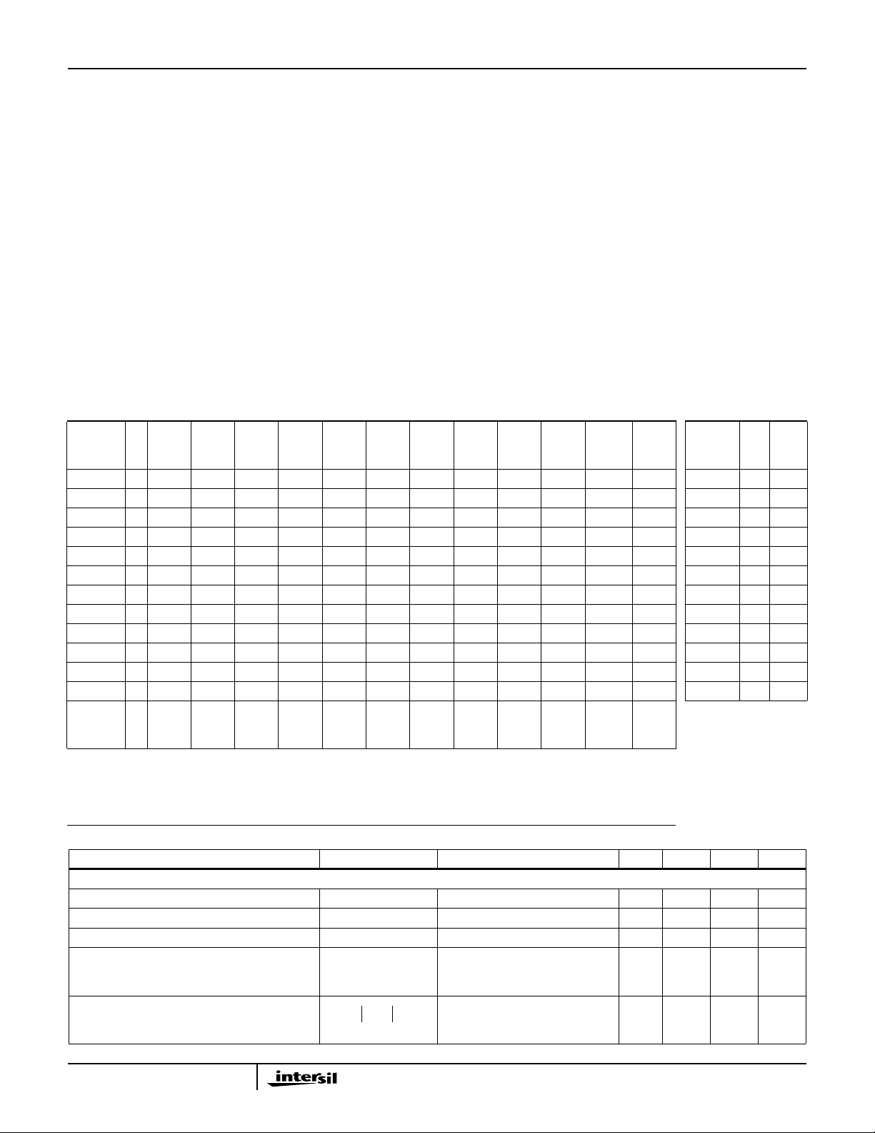
Maximum Voltage Ratings
The followingchart givesthe range of voltages which can be applied to the terminals listed verticallywith respect to the terminals listed horizontally . For example, the voltage range of the vertical Terminal 2 with respect to T erminal 4 is +15V to -5V.
(NOTE 4)
TERM
NO. 13 14 1 2 3 4 6 7 8 9 11 12 5
13 0, -20 Note 3 +5, -5 Note 3 +15, -5 Note 3 Note 3 Note 3 Note 3 Note 3 Note 3 Note 3 13 5 0.1
14 Note 3 Note 3 Note 3 +20, 0 Note 3 Note 3 Note 3 Note 3 Note 3 Note 3 +20, 0 14 50 0.1
1 +20, 0 Note 3 +20, 0 Note 3 Note 3 Note 3 Note 3 Note 3 Note 3 +20, 0 1 50 0.1
2 Note 3 +15,-5 Note 3 Note 3 Note 3 Note 3 Note 3 Note 3 Note 3 2 5 0.1
3 +1, -5 Note 3 Note 3 Note 3 Note 3 Note 3 Note 3 Note 3 3 5 0.1
4 Note 3 Note 3 Note 3 Note 3 Note 3 Note 3 Note 3 4 0.1 50
6 0, -20 Note 3 +5, -5 Note 3 +15, -5 Note 3 6 5 0.1
7 Note 3 Note 3 Note 3 Note 3 +20, 0 7 50 0.1
8 +20, 0 Note 3 Note 3 +20, 0 8 50 0.1
9 Note 3 +15, -5 Note 3 9 5 0.1
11 -1, -5 Note 3 11 5 0.1
12 Note 3 12 0.1 50
5 Ref.
Sub-
strate
NOTES:
3. Voltages are not normally applied between these terminals. Voltages appearing between these terminals will be safe
if the specified limits between all other terminals are not exceeded.
4. Terminal No. 10 of CA3054 is not used.
Maximum
Current Ratings
(NOTE 4)
TERM
NO.
I
IN
mA
I
OUT
mA
Electrical Specifications T
= 25oC
A
PARAMETER SYMBOL TEST CONDITIONS MIN TYP MAX UNIT
DC CHARACTERISTICS For Each Differential Amplifier
Input Offset Voltage (Figure 8) V
Input Offset Current (Figure 9) I
Input Bias Current (Figure 5) I
Quiescent Operating Current Ratio
(Figure 5)
I
C(Q1)
----------------- -
I
C(Q2)
Temperature Coefficient Magnitude of
Input Offset Voltage (Figure 7)
2
IO
IO
I
or
∆V
IO
-----------------
∆T
I
C(Q5)
----------------- -
I
C(Q6)
VCB = 3V, I
VCB = 3V, I
VCB = 3V, I
= 3V, I
V
CB
= 3V, I
V
CB
E(Q3)
E(Q3)
E(Q3)
E(Q3)
E(Q3)
= I
= I
= I
= I
= I
= 2mA - 0.45 5 mV
E(Q4)
= 2mA - 0.3 2 µA
E(Q4)
= 2mA - 10 24 µA
E(Q4)
= 2mA - 0.98 to
E(Q4)
1.02
= 2mA - 1.1 - µV/oC
E(Q4)
--

CA3054
Electrical Specifications T
= 25oC (Continued)
A
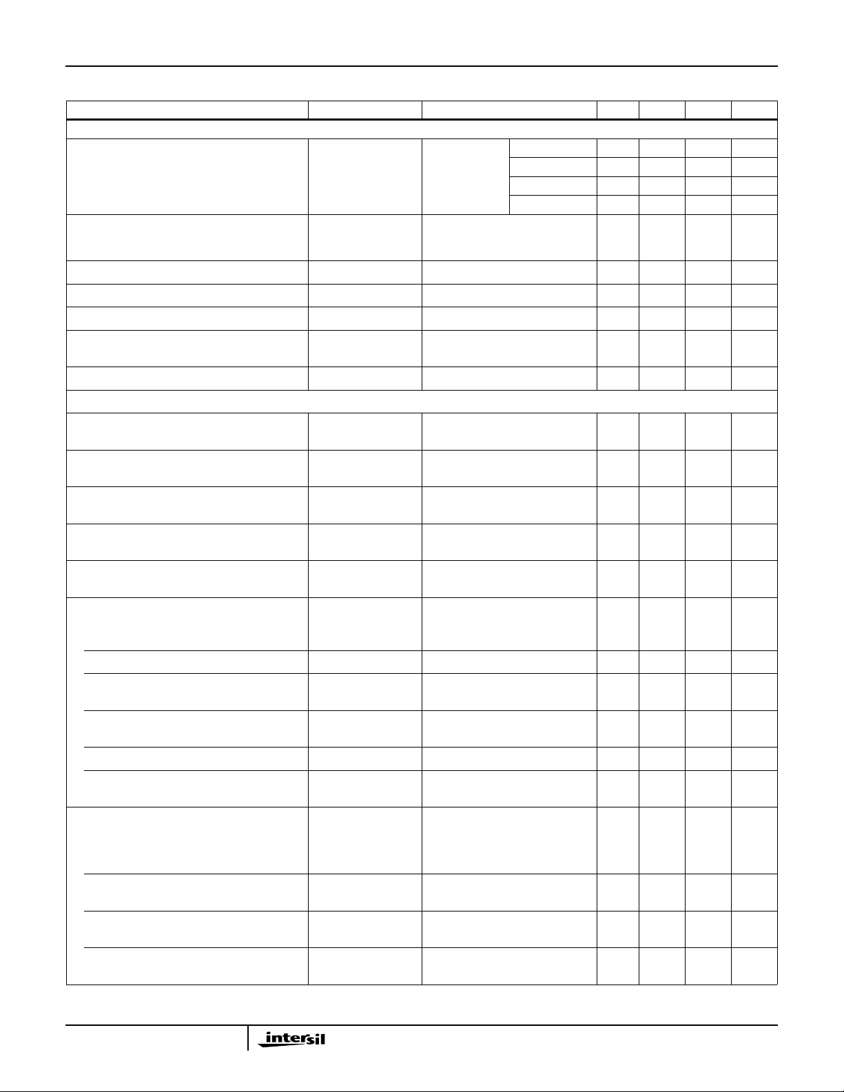
PARAMETER SYMBOL TEST CONDITIONS MIN TYP MAX UNIT
FOR EACH TRANSISTOR
DC Forward Base-to-Emitter Voltage
V
BE
(Figure 8)
Temperature Coefficient of Base-to-Emitter
Voltage (Figure 6)
Collector Cutoff Current (Figure 4) I
Collector-to-Emitter Breakdown Voltage V
Collector-to-Base Breakdown Voltage V
Collector-to-Substrate Breakdown
Voltage
Emitter-to-Base Breakdown Voltage V
∆V
BE
--------------- -
∆T
CBO
(BR)CEO
(BR)CBO
V
(BR)CIO
(BR)EBO
DYNAMIC CHARACTERISTICS
Common Mode Rejection Ratio for each
CMRR V
Amplifier (Figures 1, 10)
AGC Range, One Stage (Figures 2, 11) AGC V
Voltage Gain, Single Stage Double-Ended
AV
Output (Figures 2, 11)
AGC Range, Two Stage (Figures 3, 12) AGC V
Voltage Gain, Two Stage Double-Ended Output
AV
(Figures 3, 12)
LowFrequency ,SmallSignal EquivalentCircuitChar-
acteristics (For Single Transistor)
Forward Current Transfer Ratio (Figure 13) h
Short Circuit Input Impedance (Figure 13) h
Open Circuit Output Impedance
FE
IE
h
OE
(Figure 13)
Open Circuit Reverse Voltage Transfer
Ratio (Figure 13)
h
RE
1/f Noise Figure for Single Transistor NF f = 1kHz, V
Gain Bandwidth Product for Single
f
T
Transistor (Figure 14)
Admittance Characteristics; Differential
Circuit Configuration (For Each Amplifier)
Forward Transfer Admittance (Figure 15) Y
Input Admittance (Figure 16) Y
Output Admittance (Figure 17) Y
Reverse Transfer Admittance (Figure 18) Y
21
11
22
12
VCB = 3V IC = 50µA - 0.630 0.700 V
= 1mA - 0.715 0.800 V
I
C
I
= 3mA - 0.750 0.850 V
C
= 10mA - 0.800 0.900 V
I
C
= 3V, IC = 1mA - -1.9 - µV/oC
V
CB
VCB = 10V, IE = 0 - 0.002 100 nA
IC = 1mA, IB = 0 15 24 - V
IC = 10µA, IE = 0 20 60 - V
IC = 10µA, ICI = 0 20 60 - V
IE = 10µA, IC = 0 5 7 - V
= 12V, VEE = -6V,
CC
- 100 - dB
VX = -3.3V, f = 1kHz
= 12V, VEE = -6V,
CC
-75-dB
VX = -3.3V, f = 1kHz
= 12V, VEE = -6V,
CC
-32-dB
VX = -3.3V, f = 1kHz
= 12V, VEE = -6V,
CC
- 105 - dB
VX = -3.3V, f = 1kHz
= 12V, VEE = -6V,
CC
-60-dB
VX = -3.3V, f = 1kHz
f = 1kHz, VCE = 3V, IC = 1mA - 110 - f = 1kHz, VCE = 3V, IC = 1mA - 3.5 - kΩ
f = 1kHz, VCE = 3V, IC = 1mA - 15.6 - µS
f = 1kHz, VCE = 3V, IC = 1mA - 1.8 x
10
= 3V - 3.25 - dB
CE
-4
--
VCE = 3V, IC = 3mA - 550 - MHz
VCB = 3V, f = 1MHz
Each Collector I
C
VCB = 3V, f = 1MHz
Each Collector I
C
VCB = 3V, f = 1MHz
Each Collector I
C
VCB = 3V, f = 1MHz
Each Collector I
C
≈ 1.25mA
≈ 1.25mA
≈ 1.25mA
≈ 1.25mA
- -20 + j0 - mS
- 0.22 +
-mS
j0.1
- 0.01 +
-mS
j0
- -0.003
-mS
+ j0
3
 Loading...