Intersil Corporation CA3045 Datasheet

CA3045, CA3046
Data Sheet September 1998 File Number 341.4
General Purpose NPN Transistor Arrays
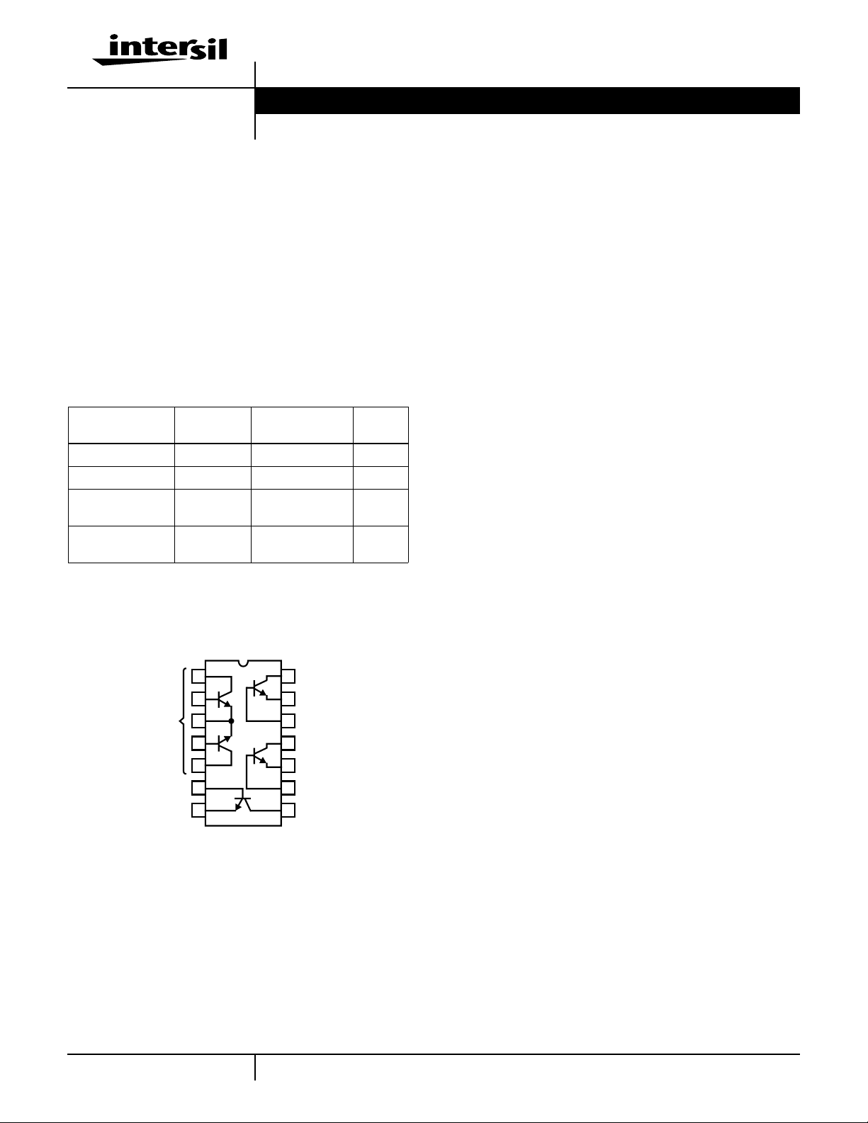
The CA3045 and CA3046 each consist of five general
purpose silicon NPN transistors on a common monolithic
substrate. Two of the transistors are internally connected to
form a differentially connected pair.
The transistors of the CA3045 and CA3046 are wellsuitedto
a wide variety ofapplicationsinlowpowersystems in the DC
through VHF range. They may be used as discrete
transistors in conventional circuits. However,in addition, they
provide the very significant inherent integrated circuit
advantages of close electrical and thermal matching.
Ordering Information
PART NUMBER
(BRAND)
CA3045F -55 to 125 14 Ld CERDIP F14.3
CA3046 -55 to 125 14 Ld PDIP E14.3
CA3046M
(3046)
CA3046M96
(3046)
TEMP.
RANGE (oC) PACKAGE
-55 to 125 14 Ld SOIC M14.15
-55 to 125 14 Ld SOIC Tape
and Reel
PKG.
M14.15
NO.
Features
• Two Matched Transistors
-V
Match . . . . . . . . . . . . . . . . . . . . . . . . . . . . . . ±5mV
BE
-I
Match. . . . . . . . . . . . . . . . . . . . . . . . . . . . 2µA (Max)
IO
• Low Noise Figure . . . . . . . . . . . . . . . . 3.2dB (Typ) at 1kHz
• 5 General Purpose Monolithic Transistors
• Operation From DC to 120MHz
• Wide Operating Current Range
• Full Military Temperature Range
Applications
• Three Isolated Transistors and One Differentially
Connected Transistor Pair for Low Power Applications at
Frequencies from DC Through the VHF Range
• Custom Designed Differential Amplifiers
• Temperature Compensated Amplifiers
• See Application Note, AN5296 “Application of the CA3018
Integrated-Circuit Transistor Array” for Suggested
Applications
Pinout
DIFFERENTIAL
CA3045, (CERDIP)
CA3046 (PDIP, SOIC)
TOP VIEW
1
2
PAIR
3
4
5
6
7
14
Q
5
13
Q
4
SUBSTRATE
12
11
10
9
8
Q
1
Q
2
Q
3
1
CAUTION: These devices are sensitive to electrostatic discharge; follow proper IC Handling Procedures.
1-888-INTERSIL or 321-724-7143
| Copyright © Intersil Corporation 1999

CA3045, CA3046
Absolute Maximum Ratings Thermal Information
Collector-to-Emitter Voltage (V
Collector-to-Base Voltage (V
Collector-to-Substrate Voltage (V
Emitter-to-Base Voltage (V
Collector Current (IC). . . . . . . . . . . . . . . . . . . . . . . . . . . . . . . . 50mA
Operating Conditions
Temperature Range. . . . . . . . . . . . . . . . . . . . . . . . . -55oC to 125oC
CAUTION: Stresses above those listed in “Absolute Maximum Ratings” may cause permanent damage to the device. This is a stress only rating and operation of the
device at these or any other conditions above those indicated in the operational sections of this specification is not implied.
NOTES:
1. Thecollector of each transistor of the CA3045 and CA3046 is isolated from the substrate by an integral diode. The substrate (Terminal13) must
be connected to the most negative point in the external circuit to maintain isolation between transistors and to provide for normal transistor action.
2. θJA is measured with the component mounted on an evaluation PC board in free air.
) . . . . . . . . . . . . . . . . . . . . . 15V
CEO
) . . . . . . . . . . . . . . . . . . . . . . . 20V
CBO
, Note 1). . . . . . . . . . . . . . 20V
CIO
) . . . . . . . . . . . . . . . . . . . . . . . . . 5V
EBO
Thermal Resistance (Typical, Note 2) θJA (oC/W) θJC (oC/W)
PDIP Package . . . . . . . . . . . . . . . . . . . 180 N/A
CERDIP Package. . . . . . . . . . . . . . . . . 150 75
SOIC Package . . . . . . . . . . . . . . . . . . . 220 N/A
Maximum Power Dissipation (Any One Transistor) . . . . . . . 300mW
Maximum Junction Temperature (Hermetic Packages). . . . . . . .175oC
Maximum Junction Temperature (Plastic Package) . . . . . . . .150oC
Maximum Storage Temperature Range. . . . . . . . . . -65oC to 150oC
Maximum Lead Temperature (Soldering 10s) . . . . . . . . . . . . 300oC
(SOIC - Lead Tips Only)
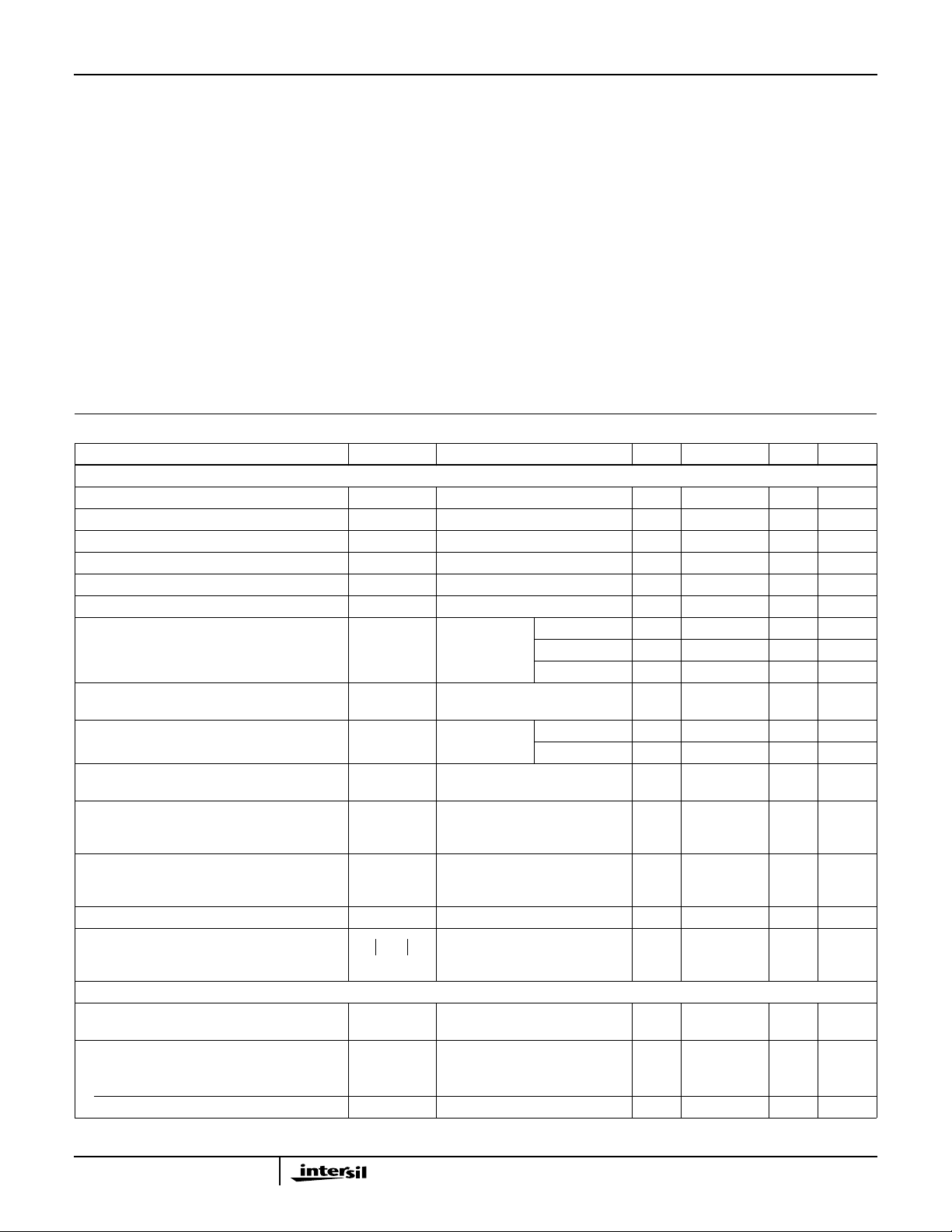
Electrical Specifications T
= 25oC, characteristics apply for each transistor in CA3045 and CA3046 as specified
A
PARAMETER SYMBOL TEST CONDITIONS MIN TYP MAX UNITS
DC CHARACTERISTICS
Collector-to-Base Breakdown Voltage V
Collector-to-Emitter Breakdown Voltage V
Collector-to-Substrate Breakdown Voltage V
Emitter-to-Base Breakdown Voltage V
Collector Cutoff Current (Figure 1) I
Collector Cutoff Current (Figure 2) I
Forward Current Transfer Ratio (Static Beta)
(Note 3) (Figure 3)
InputOffset Current for Matched PairQ1andQ2.
|I
- I
IO1
| (Note 3) (Figure 4)
IO2
Base-to-Emitter Voltage (Note 3) (Figure 5) V
MagnitudeofInputOffetVoltageforDifferentialPair
|V
- V
BE1
| (Note 3) (Figures 5, 7)
BE2
Magnitude of Input Offset Voltage for Isolated
Transistors |V
|V
- V
BE5
- V
BE4
|, |V
BE3
| (Note 3) (Figures 5, 7)
BE3
BE4
- V
BE5
|,
Temperature Coefficient of Base-to-Emitter
Voltage (Figure 6)
(BR)CBOIC
(BR)CEOIC
(BR)CIOIC
(BR)EBOIE
CBO
CEO
h
FE
BE
∆V
BE
-------------- -
∆T
= 10µA, IE = 0 20 60 - V
= 1mA, IB = 0 15 24 - V
= 10µA, ICI = 0 20 60 - V
= 10µA, IC = 0 5 7 - V
VCB = 10V, IE = 0 - 0.002 40 nA
VCE = 10V, IB = 0 - See Fig. 2 0.5 µA
VCE = 3V IC = 10mA - 100 - -
IC = 1mA 40 100 - IC = 10µA-54--
VCE = 3V, IC = 1mA - 0.3 2 µA
VCE = 3V IE = 1mA - 0.715 - V
IE = 10mA - 0.800 - V
VCE = 3V, IC = 1mA - 0.45 5 mV
VCE = 3V, IC = 1mA - 0.45 5 mV
VCE = 3V, IC = 1mA - -1.9 - mV/oC
Collector-to-Emitter Saturation Voltage V
Temperature Coefficient: Magnitude of Input Off-
set Voltage (Figure 7)
CES
∆V
----------------
∆T
IB = 1mA, IC = 10mA - 0.23 - V
VCE = 3V, IC = 1mA - 1.1 - µV/oC
IO
DYNAMIC CHARACTERISTICS
Low Frequency Noise Figure (Figure 9) NF f = 1kHz, VCE = 3V, IC = 100µA,
Source Resistance = 1kΩ
Low Frequency, Small Signal Equivalent
Circuit Characteristics
Forward Current Transf er Ratio (Figure 11) h
Short Circuit Input Impedance (Figure 11) h
FE
IE
f = 1kHz, VCE = 3V, IC = 1mA - 110 - f = 1kHz, VCE = 3V, IC = 1mA - 3.5 - kΩ
2
- 3.25 - dB
 Loading...