CA3039
November 1996
Features
• Six Matched Diodes on a Common Substrate
• Excellent Reverse Recovery Time . . . . . . . . . 1ns (Typ)
Match . . . . . . . . . . . . . . . . . . . . . . . . . . . . 5mV (Max)
•V
F
• Low Capacitance . . . . . . C
= 0.65pF (Typ) at VR = -2V
D
Applications
• Ultra-Fast Low Capacitance Matched Diodes for
Applications in Communications and Switching
Systems
• Balanced Modulators or Demodulators
• Ring Modulators
• High Speed Diode Gates
• Analog Switches
Diode Array
Description
The CA3039 consists of six ultra-fast, low capacitance
diodes on a common monolithic substrate. Integrated circuit
construction assures excellent static and dynamic matching
of the diodes, making the array extremely useful for a wide
variety of applications in communication and switching
systems.
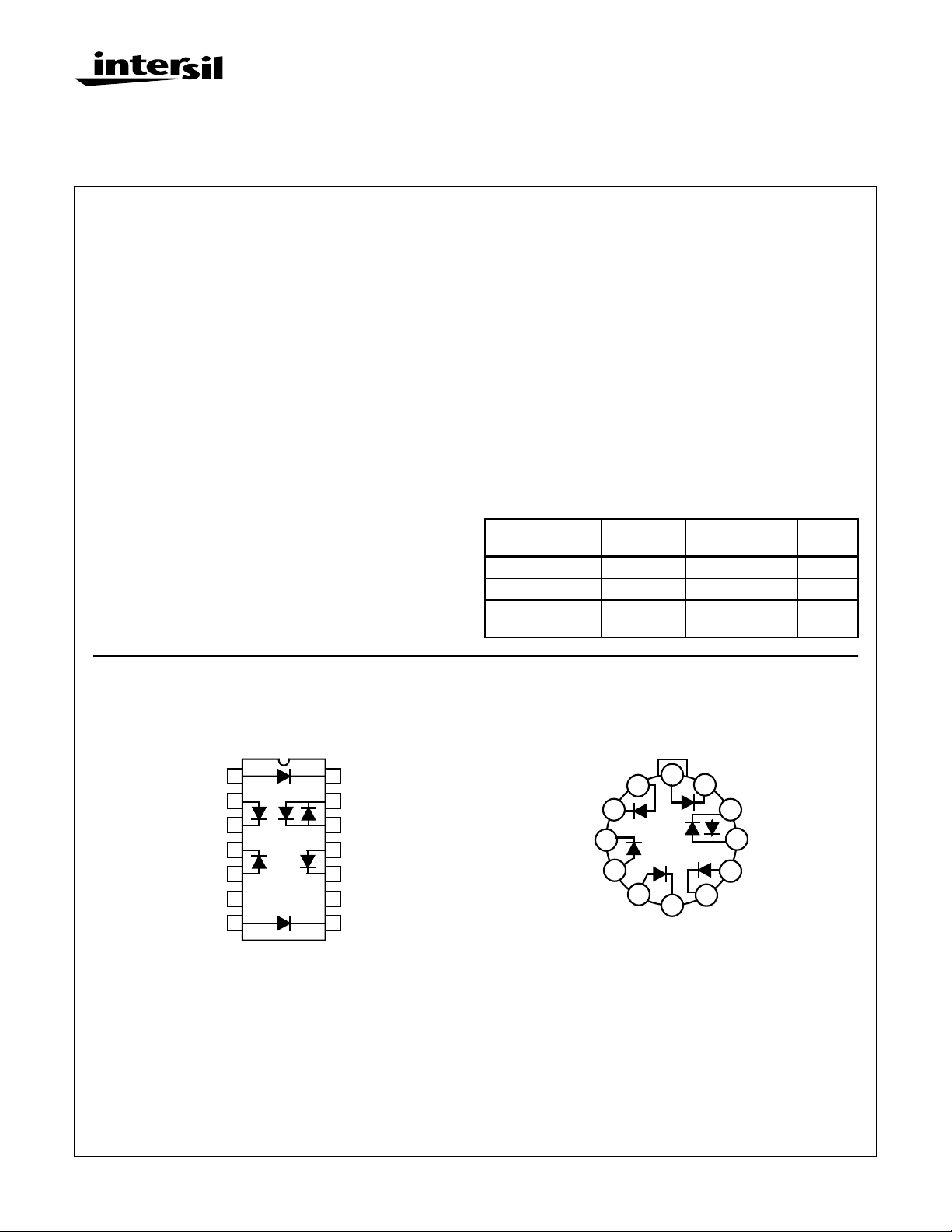
Five of the diodes are independently accessible, the sixth
shares a common terminal with the substrate.
For applications such as balanced modulators or ring
modulators where capacitive balance is important, the
substrate should be returned to a DC potential which is
significantly more negative (with respect to the active diodes)
than the peak signal applied.
Ordering Information
TEMP.
PART NUMBER
CA3039 -55 to 125 12 Pin Metal Can T12.B
CA3039M -55 to 125 14 Ld SOIC M14.15
CA3039M96 -55 to 125 14 Ld SOIC Tape
RANGE (oC) PACKAGE
and Reel
PKG.
NO.
M14.15
Pinouts
NC
CA3039
(SOIC)
TOP VIEW
1
2
3
D
4
4
5
D
3
6
7
CA3039
(METAL CAN)
TOP VIEW
D
D
14
5
13
SUBSTRATE
12
D
6DS
11
10
D
1
NC
9
2
8
2
3
4
12
1
D
4
D
3
D
5
11
D
5
D
2
6
10
6
D
9
D
S
1
8
7
CAUTION: These devices are sensitive to electrostatic discharge; follow proper IC Handling Procedures.
1-888-INTERSIL or 321-724-7143
| Copyright © Intersil Corporation 1999
7-18
File Number 343.3

CA3039
Absolute Maximum Ratings Thermal Information
Inverse Voltage (PIV) for: D1 - D5 . . . . . . . . . . . . . . . . . . . . . . . . 5V
D6. . . . . . . . . . . . . . . . . . . . . . .0.5V
Diode-to-Substrate Voltage (VDI) for D1 - D5. . . . . . . . . . . .20V, -1V
(Terminal 1, 4, 5, 8 or 12 to Terminal 10)
DC Forward Current (IF). . . . . . . . . . . . . . . . . . . . . . . . . . . . . .25mA
Recurrent Forward Current (IF) . . . . . . . . . . . . . . . . . . . . . . .100mA
Forward Surge Current (I
(SURGE)
F
). . . . . . . . . . . . . . . . . . . .100mA
Operating Conditions
Temperature Range . . . . . . . . . . . . . . . . . . . . . . . . -55oC to 125oC
CAUTION: Stresses above those listed in “Absolute Maximum Ratings” may cause permanent damage to the device. This is a stress only rating and operation
of the device at these or any other conditions above those indicated in the operational sections of this specification is not implied.
NOTE:
1. θJA is measured with the component mounted on an evaluation PC board in free air.
Thermal Resistance (Typical, Note 1) θJA (oC/W) θJC (oC/W)
Metal Can Package. . . . . . . . . . . . . . . 200 120
SOIC Package. . . . . . . . . . . . . . . . . . . 220 N/A
Maximum Power Dissipation (Any One Diode) . . . . . . . . . . .100mW
Maximum Junction Temperature (Metal Can Package) . . . . . . . 175oC
Maximum Junction Temperature (Plastic Package) . . . . . . . . 150oC
Maximum Storage Temperature Range . . . . . . . . . -65oC to 150oC
Maximum Lead Temperature (Soldering 10s) . . . . . . . . . . . . 300oC
(SOIC - Lead Tips Only)
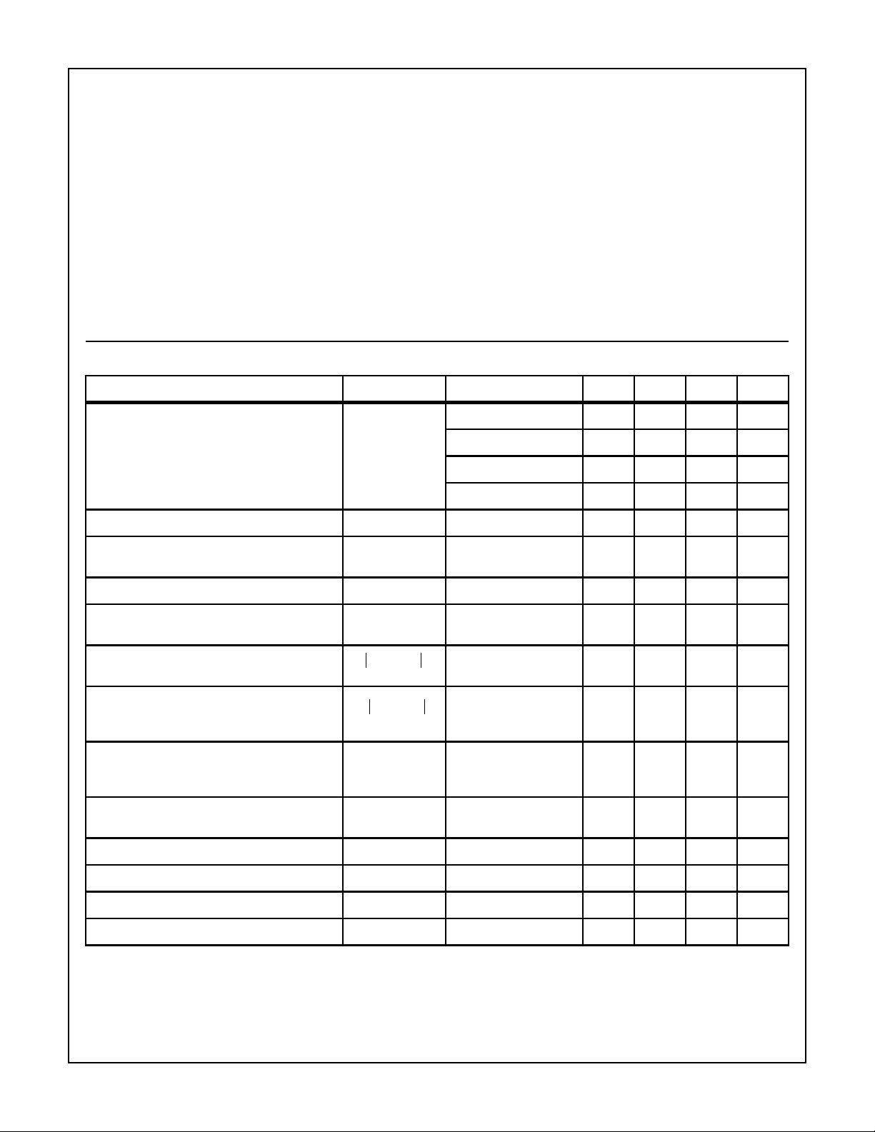
Electrical Specifications T
= 25oC; Characteristics apply for each diode unit, Unless Otherwise Specified
A
PARAMETER SYMBOL TEST CONDITIONS MIN TYP MAX UNITS
DC Forward Voltage Drop (Figure 1) V
DC Reverse Breakdown Voltage V
DC Reverse Breakdown Voltage Between Any
Diode Unit and Substrate
DC Reverse (Leakage) Current (Figure 2) I
DC Reverse (Leakage) Current Between Any
Diode Unit and Substrate (Figure 3)
Magnitude of Diode Offset Voltage (Note 2)
VF1VF2–
(Figure 1)
Temperature Coefficient of |V
- VF2| (Figure 4) IF = 1mA - 1.0 - µV/oC
F1
∆ VF1VF2–
----------------------------------
Temperature Coefficient of Forward Drop
(Figure 5)
(BR)R
V
(BR)R
∆T
∆V
-----------
∆T
F
IF = 50µA - 0.65 0.69 V
= 1mA - 0.73 0.78 V
I
F
I
= 3mA - 0.76 0.80 V
F
= 10mA - 0.81 0.90 V
I
F
IR = -10µA57-V
IR = -10µA20--V
R
I
R
F
VR = -4V - 0.016 100 nA
VR = -10V - 0.022 100 nA
I
= 1mA - 0.5 5.0 mV
F
= 1mA - -1.9 - mV/oC
I
F
DC Forward Voltage Drop for Anode-toSubstrate Diode (D
)
S
Reverse Recovery Time t
Diode Resistance (Figure 6) R
Diode Capacitance (Figure 7) C
Diode-to-Substrate Capacitance (Figure 8) C
V
RR
F
D
D
DI
IF = 1mA - 0.65 - V
IF = 10mA, IR = -10mA - 1.0 - ns
f = 1kHz, IF = 1mA 25 30 45 Ω
VR = -2V, IF = 0 - 0.65 - pF
VDI = 4V, IF = 0 - 3.2 - pF
NOTE:
2. Magnitude of Diode Offset Voltage is the difference in DC Forward Voltage Drops of any two diode units.
7-19
 Loading...