Intersil Corporation CA3020A, CA3020 Datasheet

April 1997
CA3020, CA3020A
8MHz Po wer Amps For Military,
Industrial and Commercial Equipment
[ /Title
(CA30
20,
CA302
0A)
/Subject
(8MHz
Power
Amps
For
Military,
Industrial
and
Commercial
Equipment)
/Autho
r ()
/Keywords
(Intersil
Corporation,
Semiconductor,
single,
power
amplifier,
class b
amplifier,
military
Features
• High Power Output Class B Amplifier
- CA3020 . . . . . . . . . . . . . . . . . . . . 0.5W (Typ) at V
- CA3020A . . . . . . . . . . . . . . . . . . 1.0W (Typ) at V
• Wide Frequency Range . . Up to 8MHz with Resistive Loads
• High Power Gain. . . . . . . . . . . . . . . . . . . . . . . . . 75dB (Typ)
• Single Power Supply For Class B Operation With
T ransf ormer
- CA3020 . . . . . . . . . . . . . . . . . . . . . . . . . . . . . . . . 3V to 9V
- CA3020A . . . . . . . . . . . . . . . . . . . . . . . . . . . . . . 3V to 12V
• Built-In Temperature-Tracking Voltage Regulator Provides
Stable Operation Over -55
o
C to 125oC Temperature Range
CC
CC
= 9V
= 12V
Applications
• AF Power Amplifiers For Portable and Fixed Sound and
Communications Systems
• Servo-Control Amplifiers
• Wide-Band Linear Mixers
• Video Power Amplifiers
• Transmission-Line Driver Amplifiers (Balanced and
Unbalanced)
• Fan-In and Fan-Out Amplifiers For Computer Logic Circuits
• Lamp-Control Amplifiers
• Motor-Control Amplifiers
• Power Multivibrators
• Power Switches
Pinout
CA3020
(METAL CAN)
TOP VIEW
V-
BUFFER AMP
DIFF IN3
OUTPUT 4
CAUTION: These devices are sensitive to electrostatic discharge; follow proper IC Handling Procedures.
1-888-INTERSIL or 321-724-7143 | Copyright © Intersil Corporation 1999
OUT
DIFF IN2
3
4
OUTPUT 5
2
12
1
5
6
OUTPUT 6
RB11
11
10
7
OUTPUT 7
AMP IN
9
8
BUFFER
V
CC1
RB8
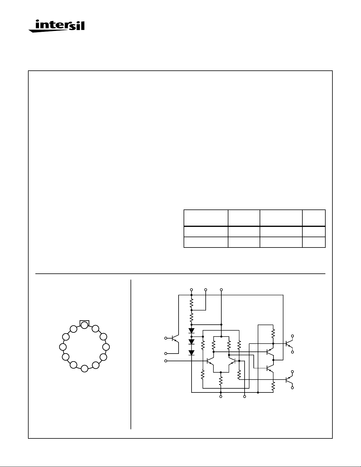
Schematic Diagram
10
1
3
The resistance values included on the schematic diagram have been supplied as a con venience to assist
Equipment Manufacturers in optimizing the selection of “outboard” components of equipment designs.
The values shown may vary as much as 30%.
Intersil reserves the right to make any changes in the Resistance Values provided such changes do not
adversely affect the published performance characteristics of the device.
Description
The CA3020 and CA3020A are integrated-circuit, multistage, multipurpose, wide-band power amplifiers on a single
monolithic silicon chip. They employ a highly versatile and
stable direct coupled circuit configuration featuring wide
frequency range, high voltage and power gain, and high
power output. These features plus inherent stability over a
wide temperature range make the CA3020 and CA3020A
extremely useful for a wide var iety of applications in militar y,
industrial, and commercial equipment.
The CA3020 and CA3020A are particularly suited for service
as class B power amplifiers. The CA3020A can provide a
maximum power output of 1W from a 12V
typical power gain of 75dB. The CA3020 provides 0.5W
power output from a 9V supply with the same power gain.
Refer to AN5766 for application inf ormation.
Ordering Information
PART NUMBER
CA3020 -55 to 125 12 Pin Metal Can T12.B
CA3020A -55 to 125 12 Pin Metal Can T12.B
98 11
R
1.5K
10
R
1.5K
11
D
1
Q
1
D
2
R4R
1
D
3
Q
R
5
10K
3-1
TEMP.
RANGE (oC) PACKAGE
R
R
3
6
Q
3
2
R
5
12K
R
2
0.47K
12 2
0.3K
supply with a
DC
PKG.
4
R
9
Q
6
Q
4
5
5
R
0.3K
6
Q
7
8
7
Q
File Number 339.5
NO.

CA3020, CA3020A
Absolute Maximum Ratings Operating Conditions
Maximum Pin 9 Supply Voltage, V
CA3020. . . . . . . . . . . . . . . . . . . . . . . . . . . . . . . . . . . . . . . . . . 10V
CA3020A. . . . . . . . . . . . . . . . . . . . . . . . . . . . . . . . . . . . . . . . . 12V
Maximum Pin 9 Supply Current, I
Maximum Pin 11 Sink Current, I11. . . . . . . . . . . . . . . . . . . . . 20mA
Output Voltage, V4 and V7 (Note 1)
CA3020. . . . . . . . . . . . . . . . . . . . . . . . . . . . . . . . . . . . . . . . . . 25V
CA3020A. . . . . . . . . . . . . . . . . . . . . . . . . . . . . . . . . . . . . . . . . 18V
Output Current, IO . . . . . . . . . . . . . . . . . . . . . . . . . . . . . . . . 300mA
Input Voltage Range, V2, V3. . . . . . . . . . . . . . . . . . . . . . . -2V to 2V
Maximum Input Voltage, V10 (Ref to Pin 1) . . . . . . . . . . . . . . . . -3V
Maximum Source Current, V1 . . . . . . . . . . . . . . . . . . . . . . . . . 1mA
CAUTION: Stresses above those listed in “Absolute Maximum Ratings” may cause permanent damage to the device. This is a stress only rating and operation
of the device at these or any other conditions above those indicated in the operational sections of this specification is not implied.
NOTES:
1. The voltage ratings for Pin 9, Pin 4 and Pin 7 are referenced to the V- (Pin 12). A normal bias configuration for Pin 8 and Pin 11 is shown
in Figure 1B. Refer to Application Note AN5766 for other options.
2. θJA is measured with the component mounted on an evaluation PC board in free air.
(Note 1)
CC1
. . . . . . . . . . . . . . . . . . 20mA
CC1
Temperature Range . . . . . . . . . . . . . . . . . . . . . . . . -55oC to 125oC
Thermal Information
Thermal Resistance (Typical, Note 2) θJA (oC/W) θJC (oC/W)
Metal Can Package. . . . . . . . . . . . . . . 165 80
Maximum Junction Temperature (Metal CanPackage). . . . . . . . 175oC
Maximum Storage Temperature Range . . . . . . . . . -65oC to 150oC
Maximum Lead Temperature (Soldering 10s). . . . . . . . . . . . 300oC
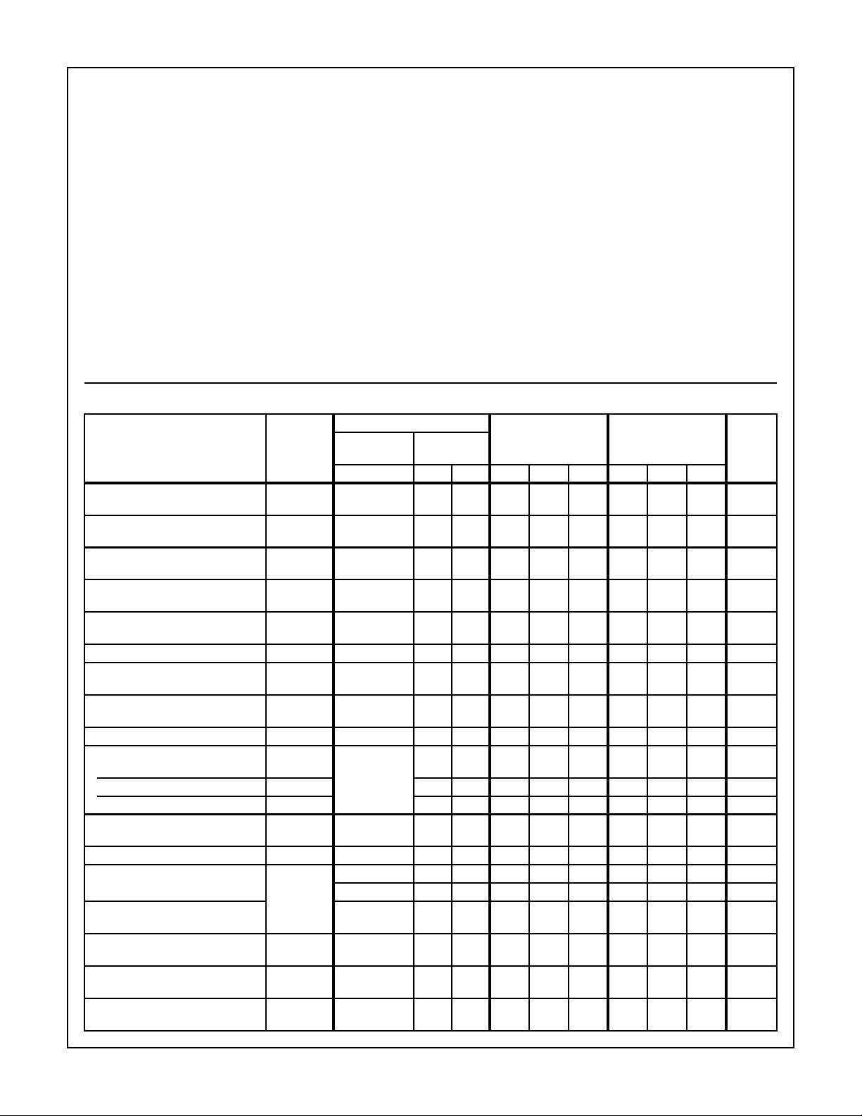
Electrical Specifications T
= 25oC
A
TEST CONDITIONS
PARAMETER SYMBOL
Collector-to-Emitter Breakdown
Voltage, Q
and Q7 at 10mA
6
Collector-to-Emitter Breakdown
Voltage, Q
Idle Currents, Q
at 0.1mA
1
and Q
6
7
V
(BR)CER
V
(BR)CEO
I4 IDLE
CIRCUIT AND
PROCEDURE
FIGURE V
1A - - 18 - - 25 - - V
- - -10- -10- - V
7 9.0 2.0 - 5.5 - - 5.5 - mA
DC SUPPLY
VOLTAGE
CC1VCC2
CA3020 CA3020A
MIN TYP MAX MIN TYP MAX
UNITS
I7 IDLE
Peak Output Currents, Q
and Q
6
7
I4PK
7 9.0 2.0 140 - - 180 - - mA
I7PK
Cutoff Currents, Q
and Q
6
7
I4 CUTOFF
7 9.0 2.0 - - 1.0 - - 1.0 mA
I7 CUTOFF
Differential Amplifier Current Drain I
Total Current Drain I
Differential Amplifier Input
Terminal Voltages
Regulator Terminal Voltage V
Cutoff (Leakage) Currents:
Q
1
Collector-to-Emitter I
Emitter-to-Base I
Collector-to-Base I
Forward Current Transfer Ratio,
Q
at 3mA
1
CC1
CC1
I
CC2
V
V
CEO
EBO
CBO
h
FE1
+
2
3
11
7 9.0 9.0 6.3 9.4 12.5 6.3 9.4 12.5 mA
7 9.0 9.0 8.0 21.5 35.0 14.0 21.5 30.0 mA
7 9.0 2.0 - 1.11 - - 1.11 - V
7 9.0 2.0 - 2.35 - - 2.35 - V
-
10.0 - - - 100 - - 100 µA
3.0 - - - 0.1 - - 0.1 µA
3.0 - - - 0.1 - - 0.1 µA
- 6.0 - 30 75 - 30 75 -
Bandwidth at -3dB Point BW 8 6.0 6.0 - 8 - - 8 - MHz
Maximum Power Output for
R
= 130Ω
CC
Maximum Power Output for
P
O(MAX)
9 6.0 6.0 200 300 - 200 300 - mW
9 9.0 9.0 400 550 - 400 550 - mW
9 9.0 12.0 - - - 800 1000 - mW
RCC = 200Ω
Sensitivity for P
OUT
= 400mW,
e
IN
9 9.0 9.0 - 35 55 - - - mV
RCC = 130Ω
Sensitivity for P
= 800mW,
OUT
e
IN
9 9.0 12.0 ----50100mV
RCC = 200Ω
Input Resistance -
Terminal 3 to Ground
R
IN3
10 6.0 6.0 - 1000 - - 1000 - Ω
3-2

CA3020, CA3020A
Typical Performance Data (Note 3) A heat sink is recommended for high ambient temperature operation.
PARAMETER SYMBOL CA3020 CA3020A UNITS
Power Supply Voltage V
Zero Signal Current Differential Amplifier I
Output Amplifier I
Maximum Signal Current Differential Amplifier I
Output Amplifier I
V
CC1
CC2
CC1
CC2
CC1
CC2
Maximum Power Output at THD = 10% PO 550 1000 mW
Sensitivity e
Power Gain G
Input Resistance R
IN
P
IN
Efficiency η 45 55 %
Signal-to-Noise Ratio S/N 70 66 dB
THD at 150mW Level 3.1 3.3 %
Test Signal Frequency from 600Ω Generator 1000 1000 Hz
Equivalent Collector-to-Collector Load Resistance R
CC
NOTE:
3. Refer to Figures 7 through 11 for measurement and symbol information.
9.0 9.0 V
9.0 12.0 V
15 15 mA
24 24 mA
16 16.6 mA
125 140 mA
35 45 mV
75 75 dB
55 55 kΩ
130 200 Ω
Test Circuits and Waveforms
V
CC
10mA
10mA
8
9
11
4
10
CA3020
CA3020A
1
2
3
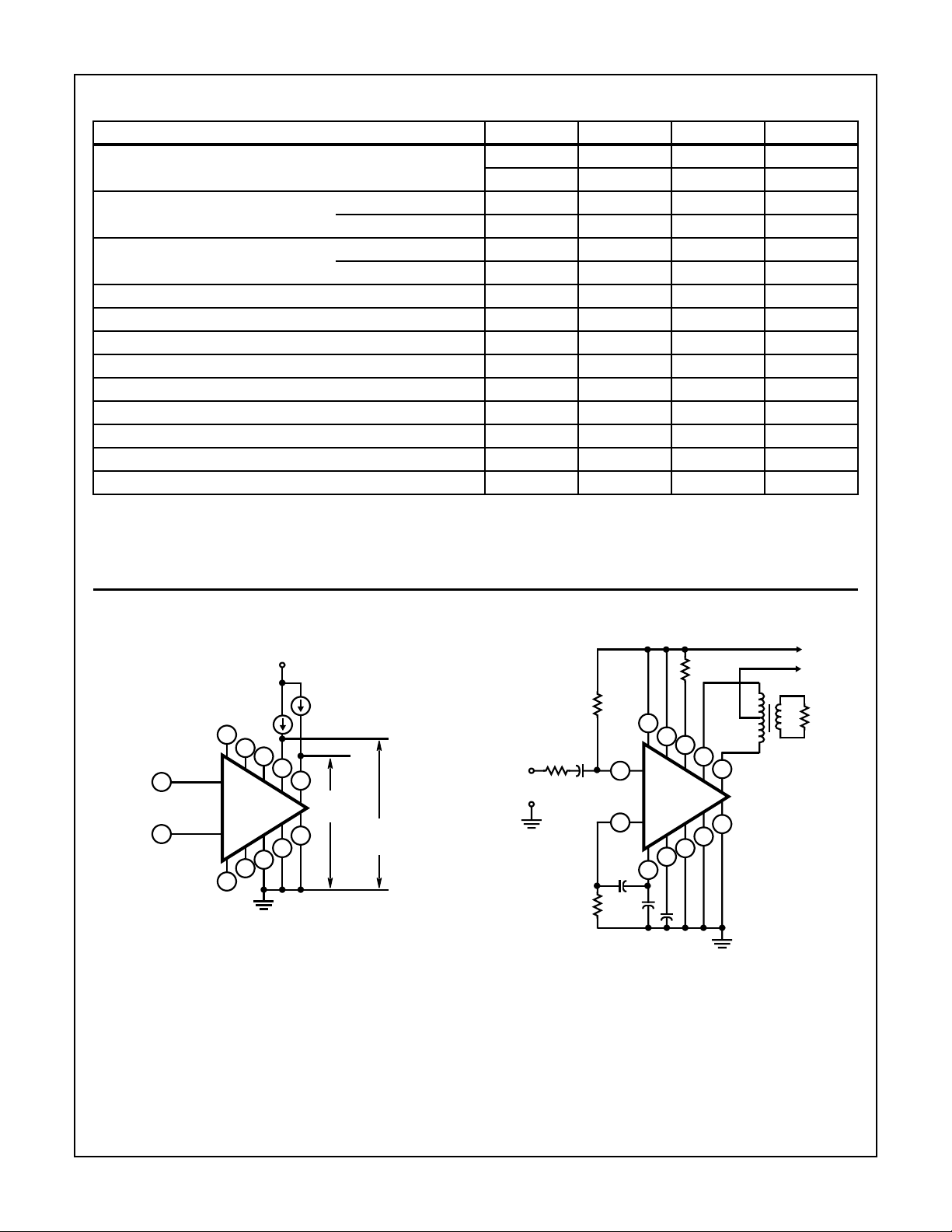
FIGURE 1A. COLLECTOR-TO-EMITTER BREAKDOWN
VOLTAGE (Q6 AND Q7) CIRCUIT
7
VBR(CER)
Q
7
(CER)
V
12
6
5
BR
Q
6
1K
510K
8
9
CA3020
CA3020A
2
3
5µF
3V
11
4
7
12
6
5
+
-
3K
+-
e
IN
~
5.1K
5µF
6V
+
10
1
5µF
3V
0.01
-
µF
FIGURE 1B. TYPICAL AUDIO AMPLIFIER CIRCUIT UTILIZING
THE CA3020 OR CA3020A AS AN AUDIO
PREAMPLIFIER AND CLASS B POWER AMPLIFIER
FIGURE 1.
V
V
CC1
CC2
3-3
 Loading...