Intersil Corporation CA2111A Datasheet

OBSOLETE PRODUCT
CA2111A
[ /Title
(CA21
11A)
/Subject
(FM
IF
AmplifierLimiter
and
Quadra
ture
Detector)
/Autho
r ()
/Keywords
(Harris
Semiconductor,
FM IF
amplifier,
quadrat
ure
detector,
limiter,
TV
audio
IF,
high
AM
rejection,
NO RECOMMENDED REPLACEMENT
May 1999
Call Central Applications 1-800-442-7747
or email: centapp@harris.com
Features
• Input Limiting Voltage At 10.7MHz . . . . . . . . . . . 400µV
• Input Limiting Voltage At 4.5, 5.5MHz . . . . . . . . 250µV
• Typical AM Rejection At 10.7MHz. . . . . . . . . . . . . 45dB
• Provision for Output fr om 3-Stage IF Amplifier Section
• Low Harmonic Distortion
• Quadrature Detection Permits Simplified Single-Coil
Tuning
• Extremely Low AFC Voltage Drift Over Full Operating
Temperature Range
• Minimum Number of External Components Required
Applications
• FM IF Sound
• TV Sound IF
Pinout
CA2111A
(PDIP)
TOP VIEW
AUDIO OUT
REF BIAS
DC FB BYPASS
INPUT BYPASS
GROUND
NC
IF IN
1
2
3
4
5
6
7
14
DE-EMPHASIS
13
V+
12
QUADRATURE INPUT
11
QUADRATURE IN BUF
10
HIGH IF OUTPUT
9
LOW IF OUTPUT
8
NC
FM IF Amplifier-Limiter
and Quadrature Detector
Description
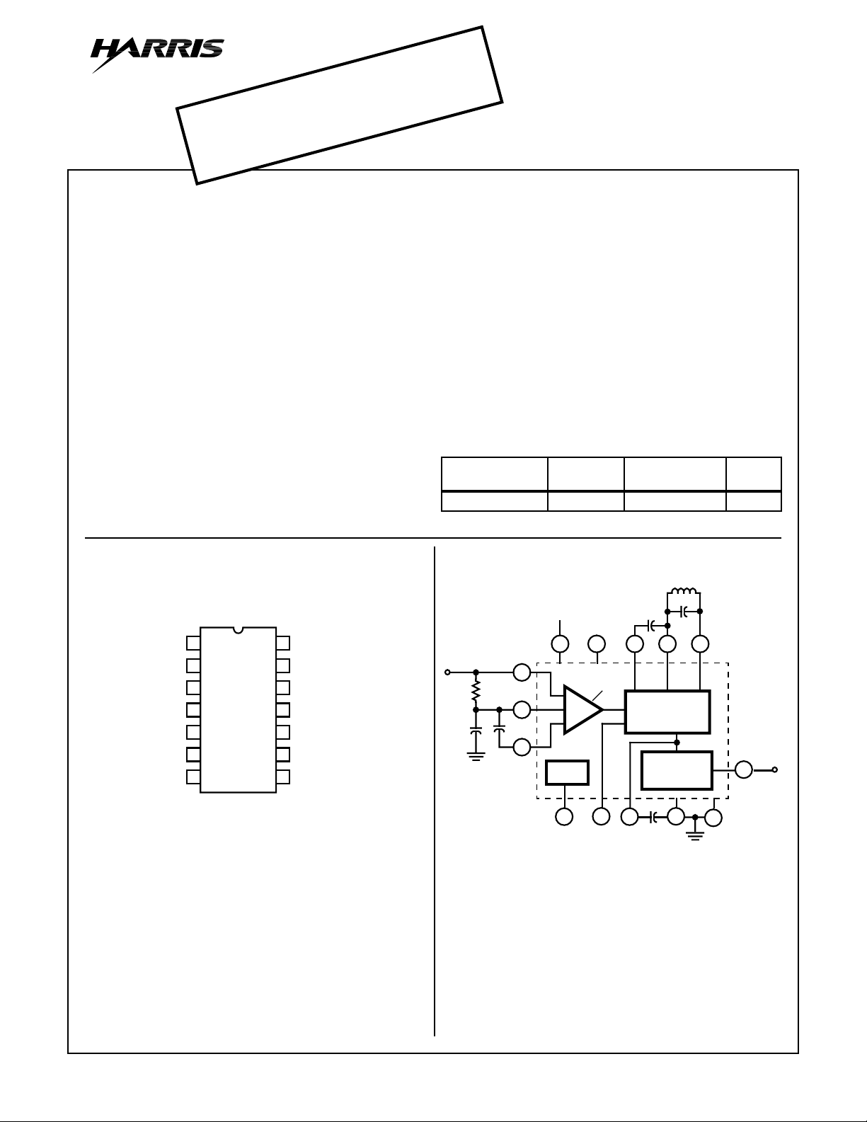
The CA2111A provides a multistage wideband amplifierlimiter, a quadrature detector, and an emitter-follower output
stage. This device is designed f or use in FM receivers and in
the sound IF sections of TV receivers. In addition, an output
terminal is provided which allows the use of the amplifierlimiter as a straight 60dB wideband amplifier.
The amplifier-limiter features the excellent limiting characteristic of 3 cascaded differential amplifiers. The quadrature
detector requires only one coil in the associated outboard
circuit and therefore, tuning is a simple procedure.
A unique feature of the CA2111A is its exceptionally low
AFC voltage drift over the full operating-temperature range.
Part Number Information
TEMP.
PART NUMBER
CA2111AE -40 to 85 14 Ld PDIP E14.3
RANGE (oC) PACKAGE
Block Diagram
L
1
0.1µF
51Ω
4
6
0.1µF
5
V+
+12V
13
AMPLIFIER-
BIAS
10
LIMITER
11
3pF
12
9
QUADRATURE
DETECTOR
EMITTER
FOLLOWER
14
0.003µF
C
1
8
PKG.
NO.
14µH
120pF
23
1
7
CAUTION: These devices are sensitive to electrostatic discharge. Users should follow proper IC Handling Procedures.
Copyright
© Harris Corporation 1999
8-13
File Number 612.2

CA2111A
Absolute Maximum Ratings T
Supply Voltage (V+ to V-). . . . . . . . . . . . . . . . . . . . . . . . . . . . . . 16V
=25oC Thermal Information
A
Thermal Resistance (Typical, Note 1) θJA (oC/W)
PDIP Package. . . . . . . . . . . . . . . . . . . . . . . . . . . . . 150
Operating Conditions
Temperature Range . . . . . . . . . . . . . . . . . . . . . . . . . . -40oC to 85oC
Supply Voltage Range (Typical) . . . . . . . . . . . . . . . . . . . . 8V to 12V
CAUTION: Stresses above those listed in “Absolute Maximum Ratings” may cause permanent damage to the device. This is a stress only rating and operation
of the device at these or any other conditions above those indicated in the operational sections of this specification is not implied.
Maximum Junction Temperature (Plastic Package) . . . . . . . . 150oC
Maximum Storage Temperature Range . . . . . . . . . -65oC to 150oC
Maximum Lead Temperature (Soldering 10s). . . . . . . . . . . . . 300oC
NOTES:
1. θJA is measured with the component mounted on an evaluation PC board in free air.
Electrical Specifications T
= 25oC Unless Otherwise Specified
A
PARAMETER SYMBOL TEST CONDITIONS MIN TYP MAX UNITS
Terminal 1 DC Voltage
Terminals 4, 5, 6, 10 DC Voltage
Terminals 2, 12 DC Voltage
Supply Current, Pin 13
Amplifier Input Resistance
Amplifier Input Capacitance
Detector Input Resistance
Detector Input Capacitance
Amplifier Output Resistance
Detector Output Resistance
De-emphasis Resistance
V
V
4, 5, 6, 10
V
2, 12
I
13
R
C
R
C
R
R
R
V+ = 12V
1
V+ = 8V
- 5.4 - V
- 3.7 - V
V+ = 8V - 1.35 - V
V+ = 8V - 3.5 - V
4
4
12
12
10
1
14
V+ = 8V
V+ = 12V
fO = 10.7MHz
-14- mA
-16- mA
-7-kΩ
-11- pF
-70- kΩ
- 2.7 - pF
-60- Ω
- 200 - Ω
- 8.8 - kΩ
DYNAMIC CHARACTERISTICS fO = 10.7MHz, ∆f = ±75kHz, V+ = 8V, FM Modulation Frequency = 400Hz, Source Resistance = 50Ω
Input Limiting Threshold Voltage
AM Rejection
Amplifier Voltage Gain
Detector Recovered Audio Output
Total Harmonic Distortion
V
I(LIM)
AMR
V
O(AF)
THD
- 400 600 µV
VI= 10mV
V
VI= 50µV
A
VI= 10mV
VI= 10mV
, 100% FM, 30% AM
RMS
RMS -55- dB
RMS - 0.3 - V
RMS -1- %
-37- dB
RMS
RMS
DYNAMIC CHARACTERISTICS fO = 10.7MHz, ∆f = ±75kHz, V+ = 12V, FM Modulation Frequency = 400Hz, Source Resistance = 50Ω
Input Limiting Threshold Voltage
AM Rejection
Amplifier Voltage Gain
Detector Recovered Audio Output
Total Harmonic Distortion
V
I(LIM)
AMR
V
O(AF)
THD
- 400 600 µV
VI= 10mV
V
VI= 50µV
A
VI= 10mV
VI= 10mV
, 100% FM, 30% AM
RMS
RMS -55- dB
RMS - 0.48 - V
RMS -1- %
-45- dB
RMS
RMS
DYNAMIC CHARACTERISTICS fO = 4.5MHz, ∆f = ±25kHz, V+ = 12V, FM Modulation Frequency = 400Hz, Source Resistance = 50Ω
Input Limiting Threshold Voltage
AM Rejection
V
I(LIM)
AMR
VI= 10mV
, 100% FM, 30% AM
RMS
- 250 400 µV
RMS
-36- dB
8-14
 Loading...