Intersil Corporation CA3524F, CA1524F, CA1524E Datasheet
CA1524, CA2524
CA2524 IS AN OBSOLETE
ODUCT
PR
October 2000
Features
• Complete PWM Power Control Circuitry
• Separate Outputs for Single-Ended or Push-Pull
Operation
• Line and Load Regulation. . . . . . . . . . . . . . . 0.2%(Typ)
• Internal Reference Supply with 1% (Max) Oscillator
and Reference Voltage Variation Over Full
Temperature Range
• Standby Current of Less Than 10mA
• Frequency of Operation Beyond 100kHz
• Variable-Output Dead Time of 0.5µs to 5µs
•Low V
Over the Temperature Range
CE(sat)
Applications
• Positive and Negative Regulated Supplies
• Dual-Output Regulators
• Flyback Converters
• DC-DC Transformer-Coupled Regulating Converters
• Single-Ended DC-DC Converters
• Variable Power Supplies
CA3524
Regulating Pulse Width Modulator
Description
The CA1524 and CA3524 are silicon monolithic integrated
circuits designed to provide all the control circuitry for use in
a broad range of switching regulator circuits.
The CA1524 and CA3524 have all the features of the industry types SG1524, SG2524, and SG3524, respectively. A
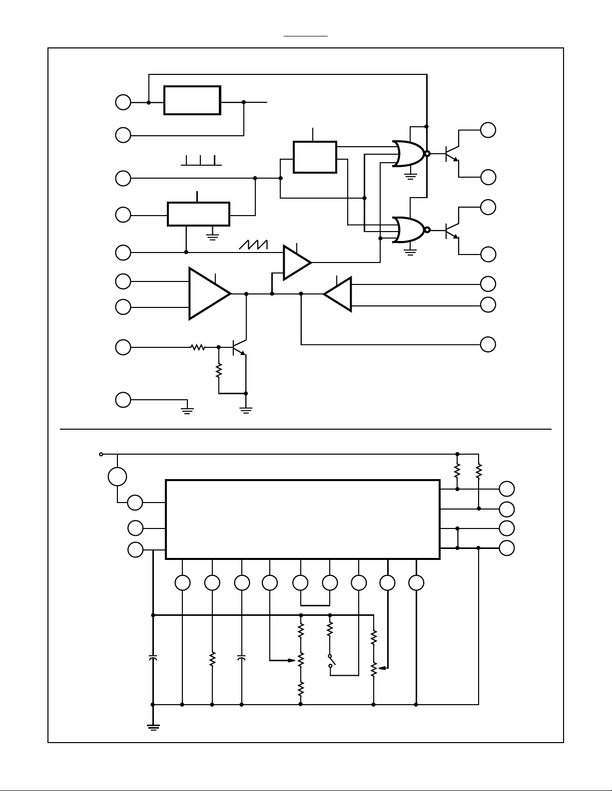
block diagram of the CA1524 series is shown in Figure 1.
The circuit includes a zener voltage reference, transconductance error amplifier, precision R-C oscillator, pulse-width
modulator, pulse-steering flip-flop, dual alternating output
switches, and current-limiting and shutdown circuitry. This
device can be used for switching regulators of either polarity,
transformer-coupled dc-dc converter, transformerless voltage doublers, dc-ac power inverters, highly efficient variable
power supplies, and polarity converter, as well as other
power-control applications.
Ordering Information
PART
NUMBER
CA1524E -55oC to +125oC 16 Lead Plastic DIP
CA1524F -55oC to +125oC 16 Lead CerDIP
CA2524E 0oC to +70oC 16 Lead Plastic DIP
CA2524F 0oC to +70oC 16 Lead CerDIP
CA3524E 0oC to +70oC 16 Lead Plastic DIP
CA3524F 0oC to +70oC 16 Lead CerDIP
TEMPERATURE
RANGE PACKAGE
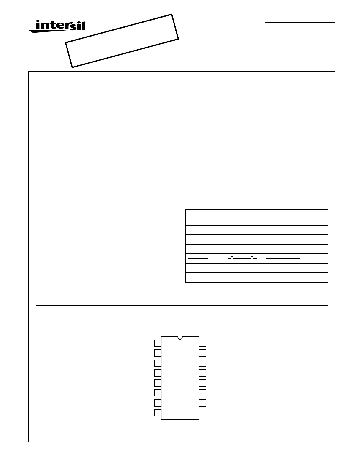
Pinout
CA1524, CA3524
(PDIP, CERDIP)
TOP VIEW
V
16
REF
15
V+
14
EMITTER B
COLLECTOR B
13
12
COLLECTOR A
EMITTER A
11
10
SHUTDOWN
COMPENSATION
9
AND COMPARATOR
NON-
R
C
GND
1
2
3
4
5
6
T
7
T
8
1
INV. INPUT
INV. INPUT
OSC OUT
(+) C.L.
SENSE
(-) C.L.
SENSE
CAUTION: These devices are sensitive to electrostatic discharge; follow proper IC Handling Procedures.
1-888-INTERSIL or 321-724-7143
| Copyright © Intersil Corporation 2000
File Number
1239.4
Functional Block Diagram
CA1524, CA2524, CA3524
15
16
3
6
7
1
2
10
V+
V
OSC OUT
R
C
INV. INPUT
NON-INV.
INPUT
REF
T
T
SHUTDOWN
REFERENCE
REGULATOR
5V
+5V
OSCILLATOR
-
ERROR
AMP
+
1kΩ
10kΩ
COMPARATOR
+5V
+5V TO ALL
INTERNAL CIRCUITS
+5V
FLIP
FLOP
+5V
+5V
C.L.
+
-
COMPENSATION AND COMPARATOR
+ SENSE
- SENSE
C
A
12
S
A
11
E
A
C
B
13
S
B
14
E
B
4
5
9
Test Circuit
8 - 40V
ls
8
0.1µF
V+
15
16
3
GND
2kΩ
1W
2kΩ
1W
OUT A
12
OUT B
13
CA1524
11
14
5410912768
2kΩ
2kΩ
R
C
T
T
10kΩ
2kΩ
10
kΩ
1kΩ
2
Specifications CA1524, CA2524, CA3524
Absolute Maximum Ratings Thermal Information
Input Voltage (Between VIN and GND Terminals). . . . . . . . . . . . 40V
Operating Voltage Range (VIN to GND) . . . . . . . . . . . . . . . .8 to 40V
Output Current Each Output:
(Terminal 11, 12 or 13, 14) . . . . . . . . . . . . . . . . . . . . . . . . .100mA
Output Current (Reference Regulator). . . . . . . . . . . . . . . . . . .50mA
Oscillator Charging Current . . . . . . . . . . . . . . . . . . . . . . . . . . . .5mA
CAUTION: Stresses above those listed in “Absolute Maximum Ratings” may cause permanent damage to the device. This is a stress only rating and operation
of the device at these or any other conditions above those indicated in the operational sections of this specification is not implied.
Thermal Resistance θ
JA
Plastic DIP Package . . . . . . . . . . . . . . . . . . . . . . . . 100oC/W
Device Dissipation
Up to TA = +25oC. . . . . . . . . . . . . . . . . . . . . . . . . . . . . . . . . 1.25W
Above TA = +25oC . . . . . . . . . . . . . . .Derate Linearly at 10mW/oC
Operating Temperature Range . . . . . . . . . . . . . . . .-55
Storage Temperature Range. . . . . . . . . . . . . . . . . . -65
o
C to +125oC
o
C to +150oC
Lead Temperature (During Soldering)
At distance 1/16 ± in. (1.59mm ±0.79mm)
from case for 10s Max. . . . . . . . . . . . . . . . . . . . . . . . . . . . +265oC
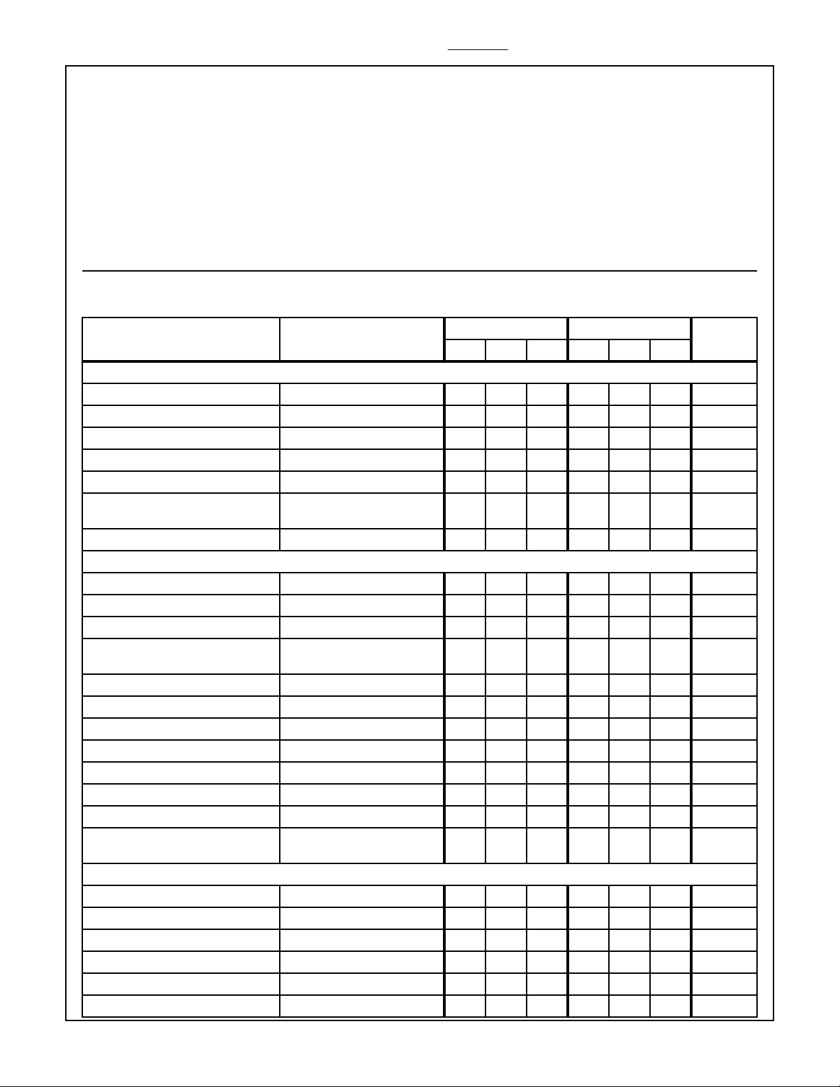
Electrical Specifications T
= -550C to +125oC for CA1524, 0oC to +70oC for the CA2524 and CA3524; V+ = 20V and
A
f = 20kHz, Unless Otherwise Stated.
CA1524, CA2524 CA3524
PARAMETER TEST CONDITIONS
UNITSMIN TYP MAX MIN TYP MAX
REFERENCE SECTION
Output Voltage 4.8 5 5.2 4.6 5 5.4 V
Line Regulation V+ = 8 to 40V - 10 20 - 10 30 mV
Load Regulation IL = 0 to 20mA - 20 50 - 20 50 mV
Ripple Rejection f = 120Hz, TA = 25oC - 66 - - 66 - db
Short Circuit Current Limit V
Temperature Stability Over Operating Temperature
= 0, TA = 25oC - 100 - - 100 - mA
REF
- 0.3 1 - 0.3 1 %
Range
Long Term Stability TA = 25oC - 20 - - 20 - mV/khr
OSCILLATOR SECTION
Maximum Frequency CT = 0.001µF, RT = 2KΩ - 300 - - 300 - kHz
Initial Accuracy RT and CT Constant - 5 - - 5 - %
Voltage Stability V+ = 8 to 40V, TA = 25oC--1--1%
Temperature Stability Over Operating Temperature
--2--2 %
Range
Output Amplitude Terminal 3, TA = 25oC - 3.5 - - 3.5 - V
Output Pulse Width (Pin 3) CT = 0.01µF, TA = 25oC - 0.5 - - 0.5 - µs
Ramp Voltage Low (Note 1) Pin 7 - 0.6 - - 0.6 - V
Ramp Voltage High (Note 1) Pin 7 - 3.5 - - 3.5 - V
Capacitor Charging Current Range Pin 7 (5-2 VBE)/R
T
0.03 - 2 0.03 - 2 mA
Timing Resistance Range Pin 6 1.8 - 120 1.8 - 120 kΩ
Charging Capacitor Range Pin 7 0.001 - 0.1 0.001 - 0.1 µF
Dead Time Expansion Capacitor on
Pin 3 100 - 1000 100 - 1000 pF
Pin 3 (when a small osc. cap is used)
ERROR AMPLIFIER SECTION
Input Offset Voltage VCM = 2.5V - 0.5 5 - 2 10 mV
Input Bias Current VCM = 2.5V - 1 10 - 1 10 µA
Open Loop Voltage Gain 72 80 - 60 80 - dB
Common Mode Voltage TA = 25oC 1.8 - 3.4 1.8 - 3.4 V
Common Mode Rejection Ratio TA = 25oC - 70 - - 70 - dB
Small Signal Bandwidth AV = 0dB, TA = 25oC - 3 - - 3 - MHz
3
Specifications CA1524, CA2524, CA3524
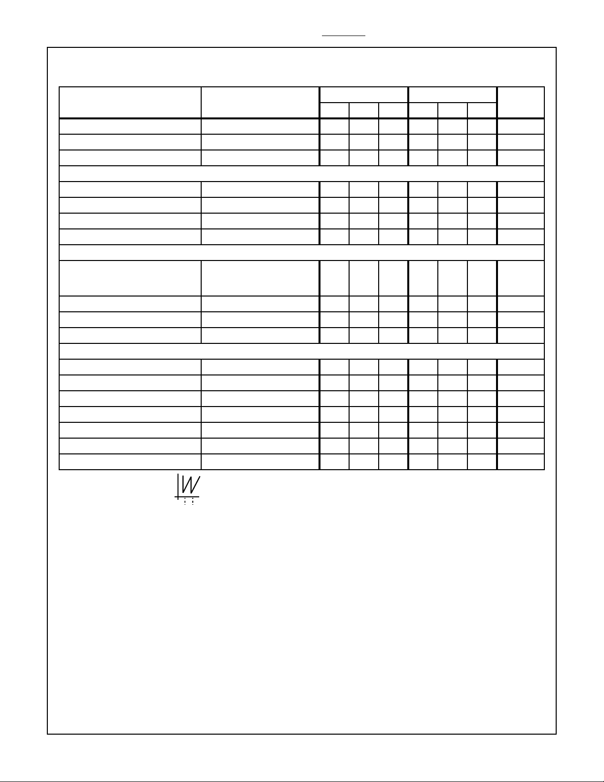
Electrical Specifications T
PARAMETER TEST CONDITIONS
Output Voltage TA = 25oC 0.5 - 3.8 0.5 - 3.8 V
Amplifier Pole - 250 - - 250 - Hz
Pin 9 Shutdown Current External Sink - 200 - - 200 - µA
COMPARATOR SECTION
Duty Cycle % Each Output On 0 - 45 0 - 45 %
Input Threshold Zero Duty Cycle - 1 - - 1 - V
Input Threshold Max. Duty Cycle - 3.5 - - 3.5 - V
Input Bias Current - 1 - - 1 - µA
CURRENT LIMITING SECTION
Sense Voltage for 25% Output Duty
Cycle
Sense Voltage T.C. - 0.2 - - 0.2 - mV/oC
Common Mode Voltage -1 - +1 -1 - +1 V
Rolloff Pole of R51 C3 + Q64 - 300 - - 300 - Hz
OUTPUT SECTION (EACH OUTUT)
Collector-Emitter Voltage 40 - - 40 - - V
Collector Leakage Current VCE = 40V - 0.1 50 - 0.1 50 µA
Saturation Voltage V+ = 40V, IC = 50mA - 0.8 2 - 0.8 2 V
Emitter Output Voltage V+ = 20V 17 18 - 17 18 - V
Rise Time RC = 2KΩ, TA = 25oC - 0.2 - - 0.2 - µs
Fall Time RC = 2KΩ, TA = 25oC - 0.1 - - 0.1 - µs
Total Standby Current: (Note 2) I
NOTES:
1. Ramp voltage at Pin 7 where t = OSC period in microseconds
Output frequency at each output transistor is half OSC frequency when each output is used separately and is equal to the OSC frequency
when each output is connected in parallel.
2. Excluding oscillator charging current, error and current limit dividers, and with outputs open.
High
Low
= -550C to +125oC for CA1524, 0oC to +70oC for the CA2524 and CA3524; V+ = 20V and
A
f = 20kHz, Unless Otherwise Stated. (Continued)
CA1524, CA2524 CA3524
Terminal 9 = 2V with Error
Amplifier Set for Max Out,
TA = 25oC
V+ = 40V - 4 10 - 4 10 mA
S
t
t ≅ RTCT with CT in microfarads and RT in ohms.
190 200 210 180 200 220 mV
UNITSMIN TYP MAX MIN TYP MAX
4
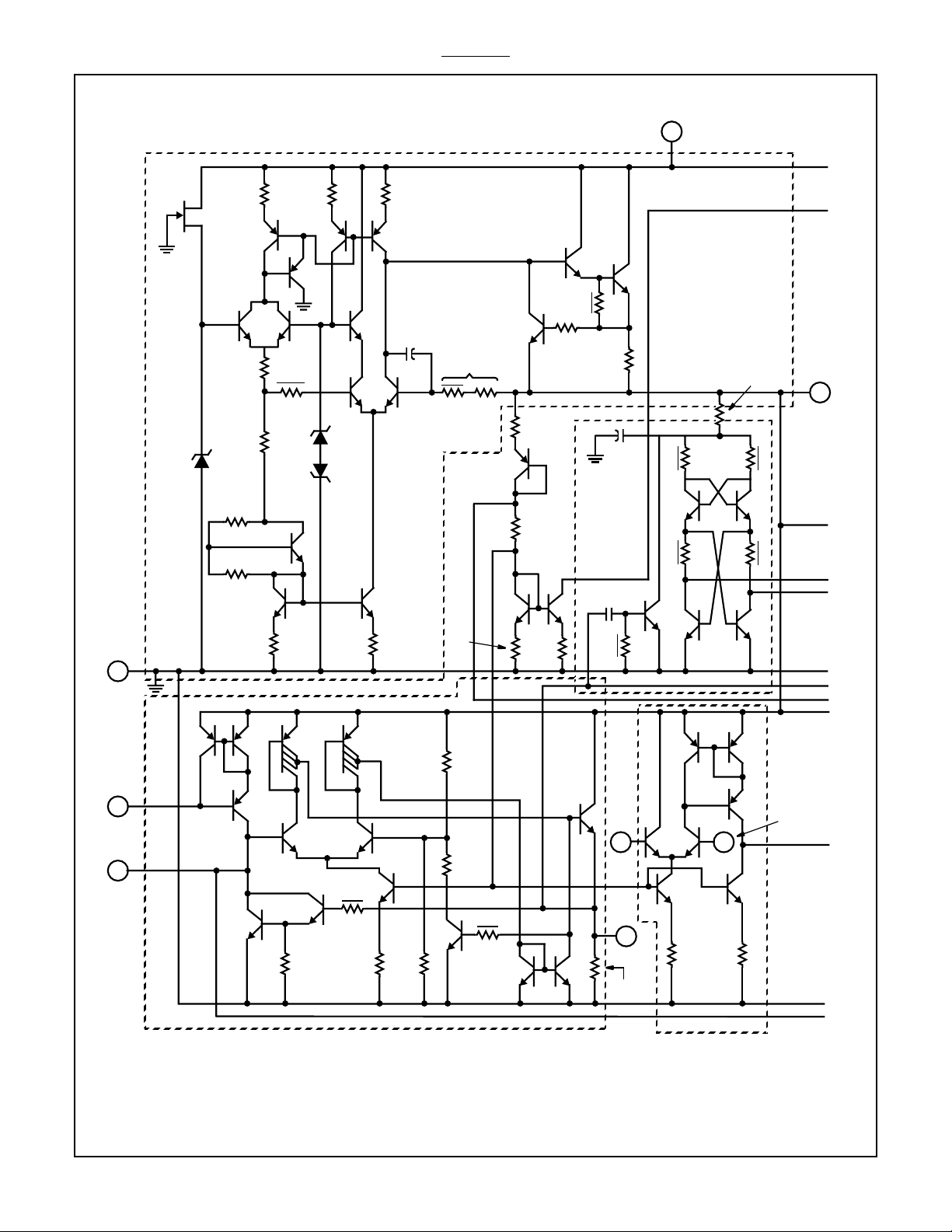
Schematic Diagram
R1
500
Q1
Q2
Q3 Q4
R2
2.7K
R3
D1
8
GND
Q42 Q43
6.3K
RA
5.3K
RB
4.8K
R4
500
CA1524, CA2524, CA3524
R5
1K
Q7
Q6
Q9
D2
R6
500
Q10
OSC SECTION
RC
10K
QA
Q5 Q12
Q47 Q48
Q13
Q11
R7
1K
20pF
C1
RD
10K 1.9K
R9
500
R43
7.4K
Q16
Q19
Q14 Q15
R14
450
R8
8.4K
R10
1K
R11
500
Q17
R12
10K
STEERING
FLIP-FLOP
N
R13
6Ω
C4
PULSE
C2
20pF
+
P
Q18
R15
25K
Q20
15
V
IN
R16
16.2K
R17
R18
18.7
18.7
K
K
Q21 Q23
R19
R18
18.7
18.7
K
K
Q22
ERROR
Q59 Q60
Q24
AMP
V
+5V
A
B
16
REF
C
D
E
F
G
H
I
6
R
T
7
C
T
Q45
Q44
Q49 Q50
Q46
R39
1K
R41
24K
R40
560
Q51
R42
19.8K
Q52
R44
1.8K
R45
25K
Q53
Q54
Q55
INV.
IN
OSC.
OUT
3
R46
3.3K
Q56 Q57
Q58 Q62
R471KR48
21
2K
Q61
NON-INV.
INPUT
J
K
L
5
 Loading...