Intersil Corporation CA1523 Datasheet

April 1994
CA1523
Voltage Regulator Control Circuit
for Variable Switching Regulator
Features
• Operates up to 200kHz
• Pins ESD Protected
• Remote ON/OFF
• Slow Start with Reset
• Overcurrent Sensing
• Lower Peak Currents than PWM Regulator
- Less Prone to Magnetic Saturation
Ordering Information
PART
NUMBER
CA1523E 0oC to +70oC 14 Lead Plastic DIP
TEMPERATURE
RANGE PACKAGE
Pinout
Description
The CA1523 monolithic silicon integrated circuit is a variable
interval pulse regulator designed to provide the control circuitry for use in switching regulator circuits. It operates from
11V to 15V.
The regulator provides a single output drive capable of
300mA source/200mA sink. The maximum operating frequency is better than 200kHz. An attractive feature of the
CA1523 is that the timing capacitor charge and discharge
current is set up externally via a single resistor. The ratio of
charge to discharge current is internally set at a maximum of
2 to 1 allowing simultaneous change in output pulse width
with increased frequency at higher load. The pulse width
variation at higher frequencies effectively compensates for
the losses in magnetics and thereby increases the power
supply efficiency at higher load end by as much as 20
percent.
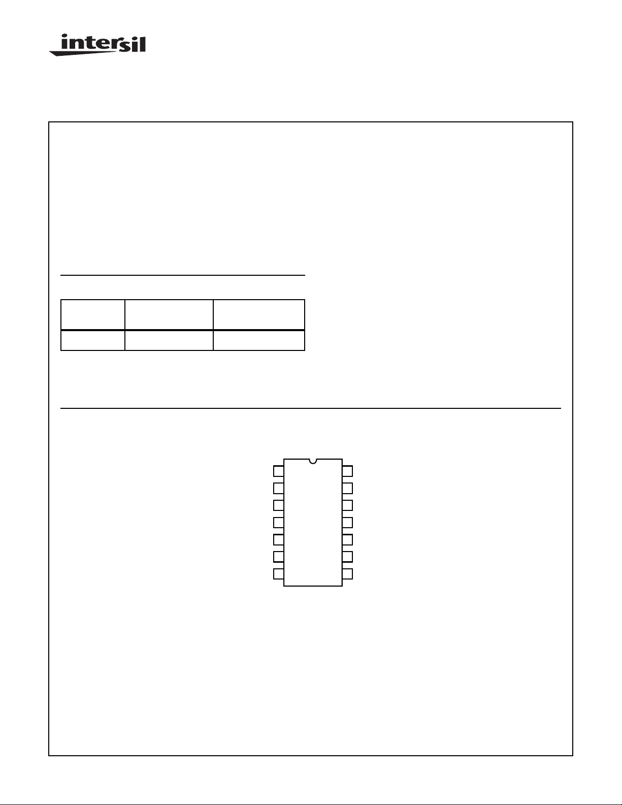
ERROR
CURRENT SENSE
GND
RISE TIME
OUTPUT GND
OUTPUT
V
CC
CA1523 (PDIP)
TOP VIEW
1
2
3
4
5
6
7
14
TIMING
13
ZENER
12
ON/OFF
11
OVER CURRENT
10
SLOW START
9
LOGIC OUTPUT
8
NC
CAUTION: These devices are sensitive to electrostatic discharge; follow proper IC Handling Procedures.
407-727-9207
| Copyright © Intersil Corporation 1999
7-11
File Number 1785.2

Specifications CA1523
Absolute Maximum Ratings Thermal Information
DC Supply Voltage. . . . . . . . . . . . . . . . . . . . . . . . . . . . . . . . . . . 15V
Supply Current
|
. . . . . . . . . . . . . . . . . . . . . . . . . . . . . . . . . . . . . . . . . . . . . .±50mA
6(MAX)
|
, 1µs,1800pF Load. . . . . . . . . . . . . . . . . . . . +300, -200mA
6(MAX)
Device Dissipation
Up to TA = 70oC . . . . . . . . . . . . . . . . . . . . . . . . . . . . . . . . 530mW
Above TA = 70oC. . . . . . . . . . . . . . . Derate Linearly at 6.7mW/oC
CAUTION: Stresses above those listed in “Absolute Maximum Ratings” may cause permanent damage to the device. This is a stress only rating and operation
of the device at these or any other conditions above those indicated in the operational sections of this specification is not implied.
Thermal Resistance θ
Plastic DIP Package . . . . . . . . . . . . . . . . . . . . . . . . 120oC/W
Device Dissipation
Up to TA = 70oC. . . . . . . . . . . . . . . . . . . . . . . . . . . . . . . . . 665mW
Ambient Temperature Range
Operating. . . . . . . . . . . . . . . . . . . . . . . . . . . . . . . . . 0oC to +70oC
Storage . . . . . . . . . . . . . . . . . . . . . . . . . . . . . . . .-55oC to +150oC
Lead Temperature (During Soldering)
At distance 1/16 ± in. (1.59mm ±0.79mm)
from case for 10s Max. . . . . . . . . . . . . . . . . . . . . . . . . . . . +265oC
JA
Electrical Specifications T
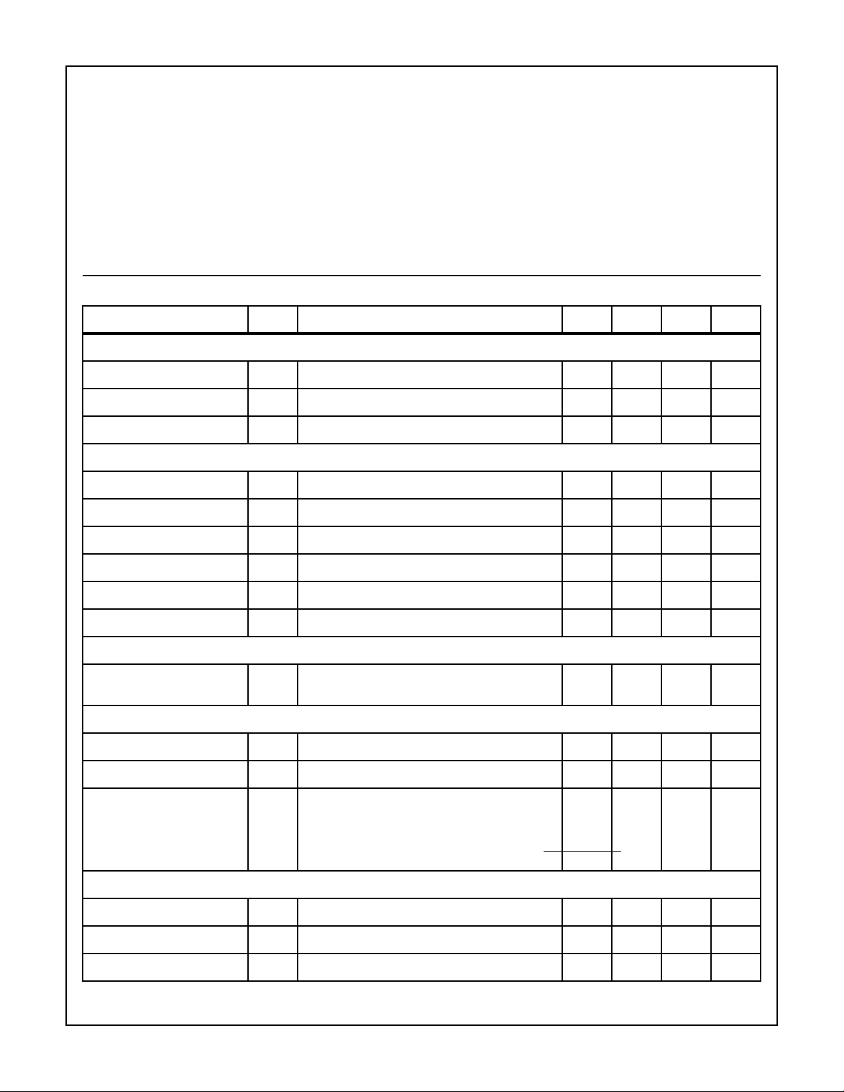
PARAMETERS PIN TEST CONDITIONS MIN TYP MAX UNITS
POWER SUPPLY, VCC (PIN 7)
Supply Voltage 7 9.5 13 - V
Supply Current 7 VCC = +13V 20 27 34 mA
Zener Voltage 13 7.8 8.4 8.9 V
OUTPUT PULSE (PIN 6)
Maximum Pulse Width 6 Measured at 6V Threshold Level 5.5 6.5 7.5 µs
Minimum Pulse Width 6 Measured at 6V Threshold Level 2 3 4 µs
Output High Voltage 6 |6 = 0mA, V4 = 0V 11.1 12 12.6 V
Output Low Voltage 6 |6 = 50mA, V12 = 0V 0.6 1 1.3 V
Rise Time 6 Measured at 1.8V and 10V Threshold Levels 250 600 1250 ns
Fall Time 6 Measured at 1.8V and 10V Threshold Levels 50 200 350 ns
ERROR VOLTAGE RANGE (PIN 1)
Error Voltage Reference 1 Adjust RT; Observe Pin 6 Min/Max
= +25oC, Refer to condition shown in test circuit; V7 = 13V, V1 = 5.9V Unless Otherwise Specified
A
5.9 6.8 7.5 V
Frequency Range
CHARGE CURRENT (PIN 14)
Charge Current 14 Adjust RT, V1 = 7.5V; Set V14 = 0V, Then V14 = 2.5V 190 220 250 µA
Discharge Current 14 Adjust RT = 5.9V; Set V14 = 5.5V, Then 5V 95 110 125 µA
Slow Start Discharge Current 14 Maintain V14 = 5V, V10 = 5.5V
Set V10 = 5.5V, Measure I14 (Hi)
Set V10 = 4V, Measure I14 (Lo)
Limits = I14 (Hi) - I14 (Lo)
1.5
LOGIC TESTS
Discharge Voltage 10 Pin 12 = 1kΩ to GND 1.7 2.4 3.2 V
Output Inhibit Voltage 7 Increase V7 Until V9≥ 2V 7.9 8.4 9.1 V
Overcurrent Trip Voltage 11 V12 = 5V; V10 = 0V; Increase V11 Until V9≤ 0.5V 1.1 1.25 1.4 V
20 30 40 µA/V
7-12
 Loading...