Intersil Corporation CA0324M96, CA0324M, CA0224M, CA0124M96, CA0124M Datasheet
...
T
C
S
B
O
M
M
O
C
E
R
O
N
D
E
D
N
E
E
T
E
L
O
A
L
P
E
R
Data Sheet May 2001
U
D
O
R
P
N
E
M
E
C
CA124, CA224, CA324, LM324, LM2902
T
File Number 796.5
Quad, 1MHz, Operational Amplifiers for
Commercial, Industrial, and Military
Applications
itle
The CA124,CA224, CA324, LM324, and LM2902 consist of
12
four independent, high-gainoperational amplifiers on a
single monolithic substrate. An on-chip capacitor in each of
224
the amplifiers provides frequency compensationfor unity
gain. These devices are designed specially to operatefrom
324
either single or dual supplies, and the differential voltage
range is equal tothe power-supplyvoltage. Low power drain
and an inputcommon-mode voltage range from 0V to V+
324
-1.5V (single-supply operation) make these devices suitable
for battery operation.
290
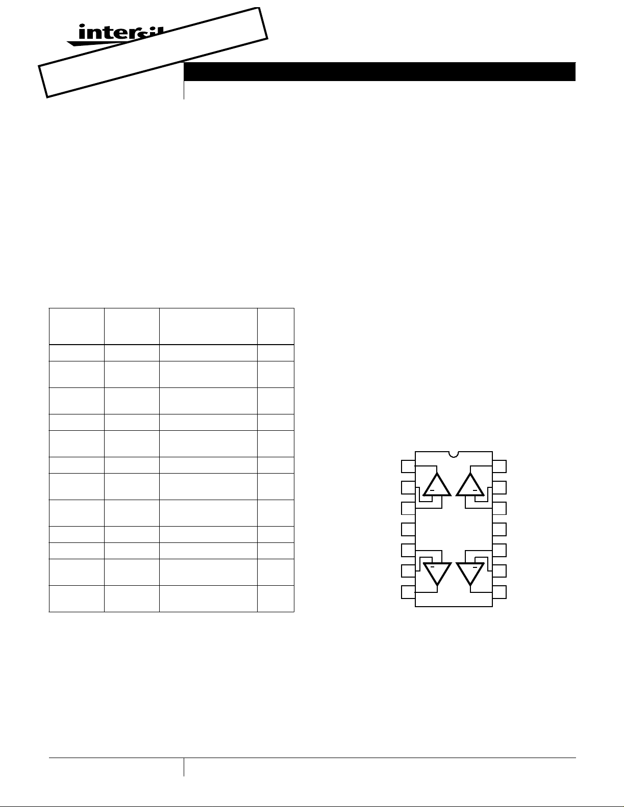
Part Number Information
b-
ad,
Hz,
ra-
al
pli-
s
-
-
,
usl,
i-
li-
s)
tho
PART
NUMBER
(BRAND)
CA0124E -55 to 125 14 Ld PDIP E14.3
CA0124M
(124)
CA0124M96
(124)
CA0224E -40 to 85 14 Ld PDIP E14.3
CA0224M
(224)
CA0324E 0 to 70 14 Ld PDIP E14.3
CA0324M
(324)
CA0324M96
(324)
LM324N 0 to70 14 Ld PDIP E14.3
LM2902N -40 to85 14 Ld PDIP E14.3
LM2902M
(2902)
LM2902M96
(2902)
TEMP.
RANGE (
o
C) PACKAGE
-55 to 125 14 Ld SOIC M14.15
-55 to 125 14 Ld SOIC Tape and
-40to85 14LdSOIC M14.15
0to70 14LdSOIC M14.15
0to70 14LdSOICTapeand
-40to85 14LdSOIC M14.15
-40to85 14LdSOICTapeand
Reel
Reel
Reel
PKG.
NO.
M14.15
M14.15
M14.15
Features
• Operation f rom Single or Dual Supplies
• Unity-GainBandwidth ...................1MHz(Typ)
• DCVoltageGain ......................100dB(Typ)
• InputBiasCurrent ......................45nA(Typ)
• InputOffsetVoltage.....................2mV(Typ)
• Input Offset Current
- CA224, CA324,LM324, LM2902 . . ........5nA(Typ)
- CA124...............................3nA(Typ)
• Replacement for Industry Types 124, 224, 324
Applications
• Summing Amplifiers
• Multivibrators
• Oscillators
• Transducer Amplifiers
• DC Gain Blocks
Pinout
CA124, CA224, CA324, LM2902 (PDIP, SOIC)
OUTPUT 1
NEG.
INPUT 1
POS.
INPUT 1
V+
POS.
INPUT 2
NEG.
INPUT 2
OUTPUT 2
LM324 (PDIP)
1
2
3
4
5
6
7
TOP VIEW
1
+
+2+
14
OUTPUT 4
13
12
11
10
9
8
NEG.
INPUT 4
POS.
INPUT 4
VPOS.
INPUT 3
NEG.
INPUT 3
OUTPUT 3
4
+
3
y-
ds
er-
1
1-888-INTERSIL or 321-724-7143
CAUTION: These devices aresensitiveto electrostatic discharge;followproperIC Handling Procedures.
| Intersil and Design is a trademarkof IntersilAmericasInc. | Copyright © Intersil Americas Inc. 2001

CA124, CA224, CA324, LM324, LM2902
Absolute Maximum Ratings Thermal Information
SupplyVoltage................................32Vor±16V
DifferentialInputVoltage...............................32V
InputVoltage.................................-0.3Vto32V
Input Current (V
OutputShort Circuit Duration(V+ ≤ 15V, Note 2) . . . . . .Continuous
<-0.3V,Note1) ......................50mA
I
Operating Co nditions
TemperatureRange
CA124 .................................-55
CA224,LM2902...........................-40
CA324,LM324..............................0
CAUTION: Stresses above those listed in “Absolute Maximum Ratings” may cause permanent damage to the device. This is a stress only rating and operationofthe
device at these or any other conditions above those indicated in the operational sections of this specification is not implied.
NOTES:
1. This inputcurrent will onlyexist when the voltage at any of theinput leads is driven negative. This currentis due to the collectorbase junction of the
input p-n-p transistorsbecoming forward biased and thereby actingas input diode clamps.In additionto this diode action, thereis also lateral n-p-n
parasitictransistor action on the ICchip.Thistransistoractioncan cause the output voltagesof the amplifiers to go totheV+voltagelevel (or to ground
for a large overdrive) for the time duration that an input is driven negative. Thistransistoraction isnot destructive and normal outputstates will reestablishwhen theinput voltage, whichwas negative, again returns to a valuegreater than -0.3V.
2. The maximum output current is approximately 40mA independentof the magnitudeof V+. Continuousshortcircuits at V+ > 15V can cause
excessive power dissipationand eventual destruction. S hort circuits from theoutput to V+ can cause overheating andeventual destruction of
the device.
3. θ
is measured with thecomponent mountedon an evaluation PC board in freeair.
JA
o
Cto125oC
o
Cto85oC
o
Cto70oC
Thermal Resistance (Typical, Note 3) θ
JA
(oC/W)
PDIPPackage............................. 95
SOICPackage............................. 175
MaximumJunctionTemperature(Die)...................175
MaximumJunctionTemperature (Plastic Package). . . . . . . . .150
MaximumStorageTemperatureRange..........-65
o
Cto150oC
MaximumLead Temperature(Soldering 10s) . . . . . . . . . .. . .300
(SOIC - LeadTips Only)
o
C
o
C
o
C
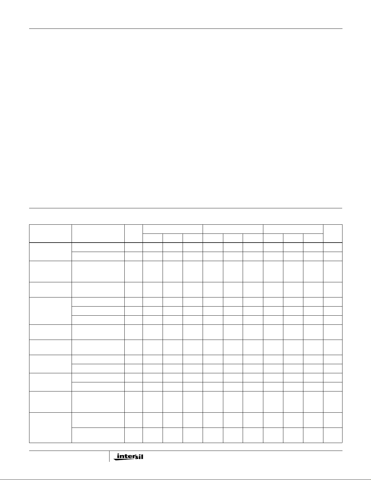
Electrical Specifications ValuesApply for EachOperational Amplifier.Supply Voltage V+ = 5V, V- = 0V,
UnlessOtherwise Specified
CA124 CA224, CA324, LM324 LM2902
PARAMETER
Input Offset
Voltage (Note 6)
Average Input
Offset Voltage
Drift
DifferentialInput
Voltage (Note 5)
Input Common
Mode Voltage
Range (Note 5)
Common Mode
Rejection Ratio
Power Supply
Rejection Ratio
InputBias
Current (Note 4)
Input Offset
Current
Average Input
Offset Current
Drift
Large Signal
Voltage Gain
TEST
CONDITIONS
TEMP.
o
C)
(
25-25-27---mV
Full--7--9--10mV
=0Ω Full-7--7--7-µV/oC
R
S
Full--V+--V+--V+V
V+ = 30V 25 0 - V+ -1.5 0 - V+ -1.5 - - - V
V+ = 30V Full 0 - V+ -2 0 - V+ -2 - - - V
V+=26V Full------0-V+-2V
DC 25 70 85 - 65 70 - - - - dB
DC 25 65 100 - 65 100 - - - - dB
I
+orII- 25 - 45 150 - 45 250 - - - nA
I
+orII- Full - - 300 - - 500 - 40 500 nA
I
I
+-II- 25- 330- 550- - -nA
I
I
+-II- Full - - 100 - - 150 - 45 200 nA
I
I
Full-10- -10- -10-pA/
R
≥ 2kΩ,V+=15V
L
(For Large V
≥ 2kΩ,V+=15V
R
L
(ForLarge V
Swing)
O
O
Swing)
25 94 100 - 88 100 - - - - dB
Full 88 - - 83 - - 83 - - dB
UNITSMIN TYP MAX MIN TYP MAX MIN TYP MAX
o
C
2

CA124, CA224, CA324, LM324, LM2902
Electrical Specifications ValuesApply for EachOperational Amplifier.Supply Voltage V+ = 5V, V- = 0V,
UnlessOtherwise Specified (Continued)
CA124 CA224, CA324, LM324 LM2902
UNITSMIN TYP MAX MIN TYP MAX MIN TYP MAX
PARAMETER
Output
Voltage
Swing
Output
Current
High
Level
Low
Level
Source V
TEST
CONDITIONS
R
=2kΩ 250-V+-1.50-V+-1.5---V
L
= 2kΩ, V+ = 30V Full 26 - - 26 - - - - - V
R
L
= 2kΩ,V+=26VFull------22--V
R
L
=10kΩ, V+ = 30V Full 27 28 - 27 28 - 23 28 - V
R
L
=10kΩ Full-520-520-5100mV
R
L
+=+1V,VI-=0V,
I
V+ = 15V
V
+=1V,VI-=0,
I
TEMP.
o
C)
(
25 20 40 - 2 0 40 - - - - mA
Full 10 20 - 10 20 - 10 20 - mA
V+ = 15V
Sink V
Crosstalk f = 1 to 20kHz
+=0V,VI-=1V,
I
V+ = 15V
+=0V,VI-=1V,
V
I
V
=200mV
O
-=1V,VI+=0,
V
I
V+ = 15V
25 10 20 - 1 0 20 - - - - mA
25 12 50 - 12 50 - - - - µA
Full58-58-58 -mA
25 - -120 - - -120 - - - - dB
(InputReferred)
Total Supply
Current
R
= ∞ Full-0.82 -0.82 -0.71.2mA
L
= ∞,V+=26VFull-------1.53mA
R
L
NOTES:
4. Due to t he PNP inputstage the directionof the input currentis out ofthe IC. No loading change existson theinput lines because the currentis
essentially constant, independentof the state ofthe output.
5. The input signal voltageand the input common mode voltageshouldnot be allowed to go negativeby more than0.3V. T he positivelimit of the
commonmode voltage range is V+ - 1.5V, but either or both inputs can go to +32V without damage.
=1.4V,RS=0Ω with V+ from5V to 30V, and over the full input common modevoltagerange (0V toV+ - 1.5V).
6. V
O
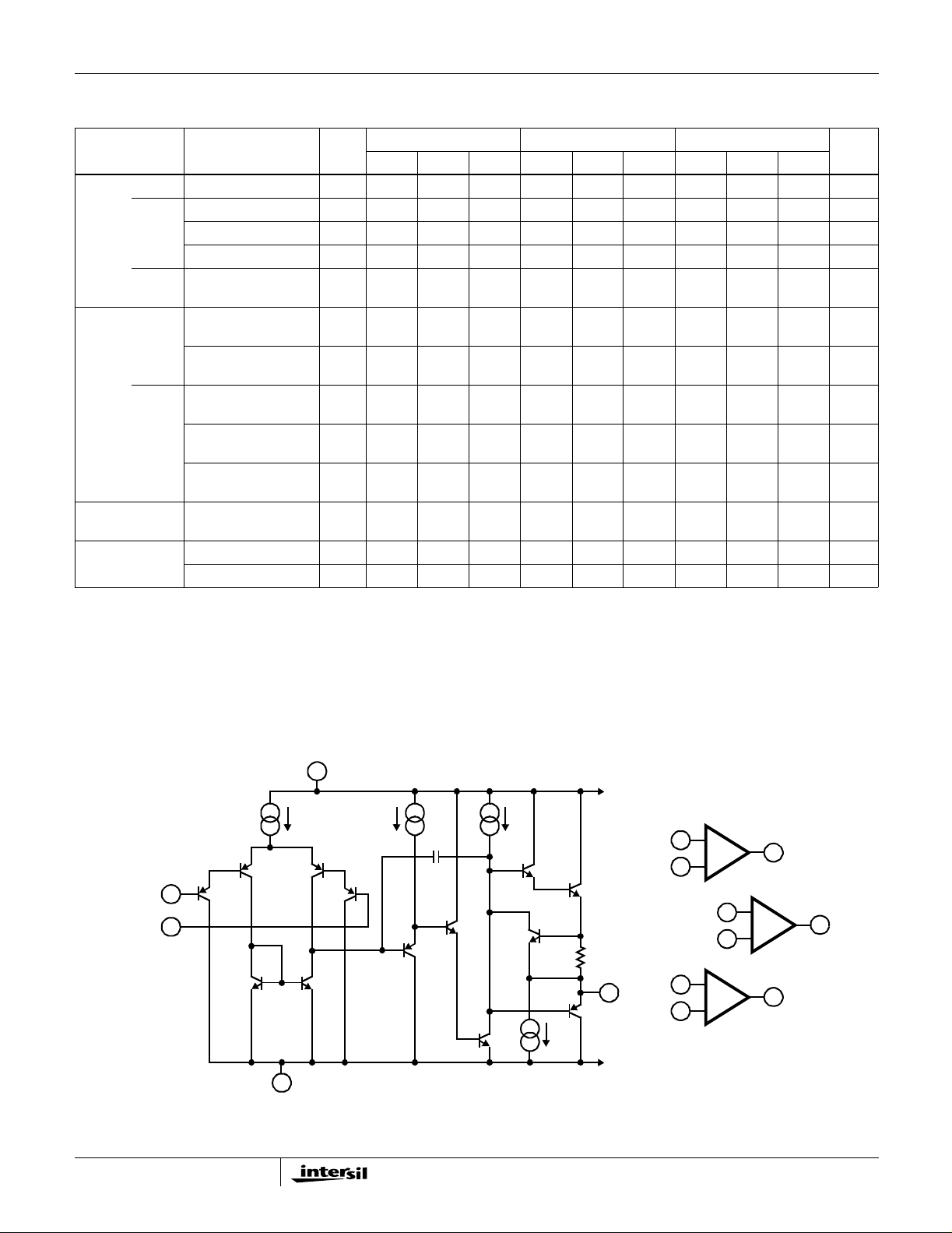
Schematic Diagram (One of FourOperational Amplifiers)
V+
4
INPUTS
6µA
Q
Q
2
-
+
Q
1
3
Q
8
3
2
Q
9
11
V-
3
4µA
C
COMP
Q
4
Q
11
Q
10
TO 2, 3, 4
100
µA
5
+
2 7
-
Q
5
Q
6
Q
7
R
SC
V
1
Q
13
Q
12
50µA
TO 2, 3, 4
6
12
+
4 4
-
13
10
O
+
3 8
-
9
 Loading...