

查询BCW60供应商
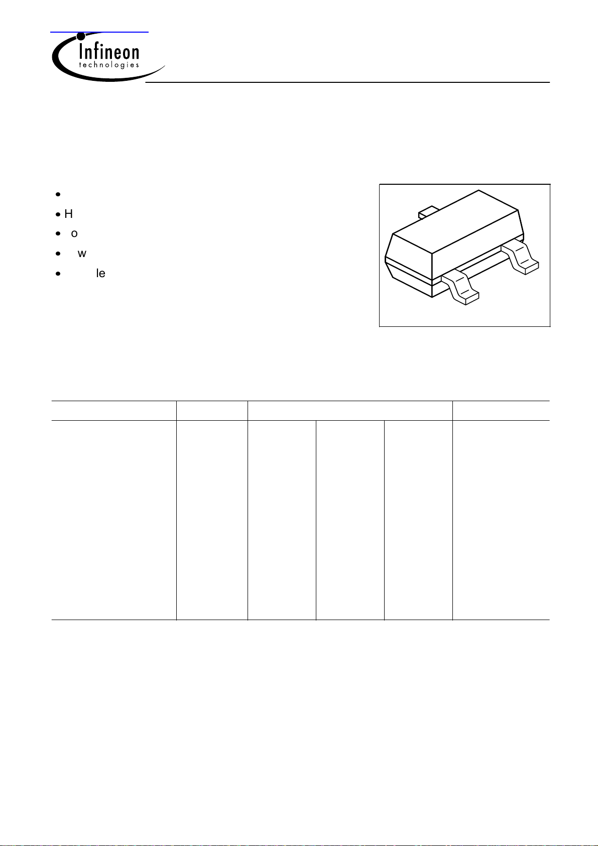
NPN Silicon AF Transistors
For AF input stages and driver applications
High current gain
Low collector-emitter saturation voltage
Low noise between 30 Hz and 15 kHz
Complementary types: BCW61, BCX71 (PNP)
BCW60, BCX70
3
1
2
VPS05161
Type Marking Pin Configuration Package
BCW60A
BCW60B
BCW60C
BCW60D
BCW60FF
BCW60FN
BCX70G
BCX70H
BCX70J
BCX70K
AAs
ABs
ACs
ADs
AFs
ANs
AGs
AHs
AJs
AKs
1 = B
1 = B
1 = B
1 = B
1 = B
1 = B
1 = B
1 = B
1 = B
1 = B
2 = E
2 = E
2 = E
2 = E
2 = E
2 = E
2 = E
2 = E
2 = E
2 = E
3 = C
3 = C
3 = C
3 = C
3 = C
3 = C
3 = C
3 = C
3 = C
3 = C
SOT23
SOT23
SOT23
SOT23
SOT23
SOT23
SOT23
SOT23
SOT23
SOT23
1 Jan-29-2002
Maximum Ratings
g
BCW60, BCX70
Parameter
Collector-emitter voltage
Collector-base voltage
Emitter-base voltage
DC collector current
Peak collector current
Peak base current
Total power dissipation, TS = 71 °C P
Junction temperature
Storage temperature
Symbol
V
CEO
V
CBO
V
EBO
I
C
I
CM
I
BM
tot
T
j
T
st
BCW60 BCW60FF BCX70
32 32 45 V
32 32 45
5 5 5
100 mA
200
200
330 mW
150 °C
-65 ... 150
Thermal Resistance
Junction - soldering point
1)
R
thJS
240 K/W
Electrical Characteristics at TA = 25°C, unless otherwise specified.
Parameter
Symbol Values Unit
min. typ. max.
Unit
DC Characteristics
Collector-emitter breakdown voltage
I
= 10 mA, IB = 0
C
Collector-base breakdown voltage
I
= 10 µA, IB = 0
C
BCW60/60FF
BCX70
BCW60/60FF
BCX70
Emitter-base breakdown voltage
I
= 1 µA, IC = 0
E
1
For calculation of R
please refer to Application Note Thermal Resistance
thJA
V
(BR)CEO
V
(BR)CBO
V
(BR)EBO
32
45
32
45
-
-
-
-
5 - -
V
-
-
-
-
2 Jan-29-2002

Electrical Characteristics at TA = 25°C, unless otherwise specified.
BCW60, BCX70
Parameter
AC Characteristics
Collector cutoff current
V
= 32 V, IE = 0
CB
= 45 V, IE = 0
V
CB
Collector cutoff current
= 32 V, IE = 0 , TA = 150 °C
V
CB
V
= 45 V, IE = 0 , TA = 150 °C
CB
Emitter cutoff current
= 4 V, IC = 0
V
EB
DC current gain 1)
= 10 µA, VCE = 5 V
I
C
BCW60 /60FF
BCX70
BCW60 / 60FF
BCX70
hFE-grp. A/ G
h
-grp. B/ H
FE
h
-grp. C/ J/ FF
FE
h
-grp. D/ K/ FN
FE
Symbol Values Unit
min. typ. max.
I
CBO
I
CBO
I
EBO
h
FE
-
-
-
-
- - 20 nA
20
20
40
100
-
-
-
-
140
200
300
460
20
20
20
20
-
-
-
-
nA
µA
-
DC current gain 1)
= 2 mA, VCE = 5 V
I
C
DC current gain 1)
= 50 mA, VCE = 1 V
I
C
hFE-grp. A/ G
h
-grp. B/ H
FE
h
-grp. C/ J/ FF
FE
h
-grp. D/ K/ FN
FE
hFE-grp. A/ G
h
-grp. B/ H
FE
h
-grp. C/ J/ FF
FE
h
-grp. D/ K/ FN
FE
h
FE
120
180
250
380
h
FE
50
70
90
100
170
250
350
500
-
-
-
-
220
310
460
630
-
-
-
-
1) Pulse test: t ≤=300µs, D = 2%
3 Jan-29-2002

Electrical Characteristics at TA = 25°C, unless otherwise specified.
BCW60, BCX70
Parameter
DC Characteristics
Collector-emitter saturation voltage1)
= 10 mA, IB = 0.25 mA
I
C
= 50 mA, IB = 1.25 mA
I
C
Base-emitter saturation voltage 1)
= 10 mA, IB = 0.25 mA
I
C
= 50 mA, IB = 1.25 mA
I
C
Base-emitter voltage 1)
= 10 µA, VCE = 5 V
I
C
I
= 2 mA, VCE = 5 V
C
= 50 mA, VCE = 1 V
I
C
AC Characteristics
Transition frequency
I
= 20 mA, VCE = 5 V, f = 100 MHz
C
Symbol Values Unit
max.typ.min.
V
CEsat
V
BEsat
V
BE(ON)
f
T
-
-
-
-
-
0.55
-
-
0.12
0.2
0.25
0.55
0.7
0.83
0.85
1.05
0.52
0.65
0.75
0.78
250 -
V
-
-
MHz
Collector-base capacitance
V
= 10 V, f = 1 MHz
CB
Emitter-base capacitance
V
= 0.5 V, f = 1 MHz
EB
Short-circuit input impedance
I
= 2 mA, VCE = 5 V, f = 1 kHz
C
Open-circuit reverse voltage transf.ratio
I
= 2 mA, VCE = 5 V, f = 1 kHz
C
hFE-grp.
A / G
B / H
C / J / FF
D / K / FN
| hFE-grp.
A / G
B / H
C / J/FF
D / K / FN
C
C
h
h
cb
eb
11e
12e
- 3
-
-
-
-
-
2.7
3.6
4.5
7.5
-
1.5
-
-
-
- pF
-8
k
-
-
-
-
10
-4
-
2
2
3
-
-
-
1) Pulse test: t ≤=300µs, D = 2%
4 Jan-29-2002

BCW60, BCX70
A
Electrical Characteristics at T
= 25°C, unless otherwise specified.
Parameter Symbol Values Unit
min. typ. max.
AC Characteristics
Short-circuit forward current transf.ratio
I
= 2 mA, VCE = 5 V, f = 1 kHz
C
Open-circuit output admittance
I
= 2 mA, VCE = 5 V, f = 1 kHz
C
Noise figure
| hFE-grp.
A / G
B / H
C / J/ FF
D / K / FN
hFE-grp.
A / G
B / H
C / J / FF
D / K / FN
hFE-grp.
h
h
F
21e
22e
-
-
-
-
-
-
-
-
200
260
330
520
18
24
30
50
-
-
-
-
-
S
-
-
-
-
dB
I
= 100 µA, VCE = 5 V, RS = 1 k,
C
f = 1 kHz, f = 200 Hz
Equivalent noise voltage
I
= 200 µA, VCE = 5 V, RS = 2 k,
C
f = 10 ... 50 Hz
A - K
FF - FN
hFE-grp.
FF / FN
V
-
-
n
- - 0.135 µV
2
1
-
2
5 Jan-29-2002

BCW60, BCX70
)
Total power dissipation P
360
mW
300
270
240
tot
P
210
180
150
120
90
60
30
0
0 15 30 45 60 75 90 105 120
= f(TS)
tot
°C
T
Collector-base capacitance C
Emitter-base capacitance C
12
C
CBO
pF
)(
C
EBO
CB
EB
= f (V
= f (V
EHP00327BCW 60/BCX 70
CBO
EBO
)
10
8
C
EBO
6
4
C
CBO
2
0
150
S
-1 1
10
0
VV
CBO
10V10
)
(
EBO
Permissible pulse load
P
totmax
P
totmax
totPDC
10
10
10
10
/ P
3
5
2
5
1
5
0
10
= f (tp)
totDC
=
D
-6
10-510-410-310
Transition frequency f
V
= 5V
CE
EHP00328BCW 60/BCX 70
t
p
t
p
T
T
D
=
3
10
MHz
f
T
= f (IC)
T
EHP00330BCW 60/BCX 70
0
0.005
0.01
0.02
0.05
10
2
0.1
0.2
-2
0.5
0
10
s
t
p
5
1
10
-1 2
10
10
0
10
1
10mA
Ι
C
6 Jan-29-2002

BCW60, BCX70
Base-emitter saturation voltage
I
= f (V
C
Ι
C
10
mA
10
5
10
5
10
2
1
0
-1
0
), hFE = 40
BEsat
100
˚C
˚C
25
-50
˚C
0.2 0.4 0.8
0.6 V 1.2
V
EHP00331BCW 60/BCX 70
BE sat
Collector-emitter saturation voltage
I
= f (V
C
Ι
C
10
mA
10
5
10
5
10
2
1
0
-1
0
), hFE = 40
CEsat
100
25
-50
0.1 0.2 0.3 0.4
˚C
˚C
˚C
V
EHP00332BCW 60/BCX 70
CEsat
V 0.5
Collector current I
V
= 5V
CE
2
10
mA
Ι
C
1
10
5
0
10
5
10
10
-1
5
-2
0
100 25 -50
= f (VBE)
C
˚C
˚C ˚C
0.5 V 1.0
DC current gain h
V
= 5V
CE
EHP00333BCW 60/BCX 70
h
FE
10
10
3
5
100
˚C
25
˚C
-50
˚C
2
= f (IC)
FE
EHP00334BCW 60/BCX 70
5
1
10
5
0
10
-2 2
10
V
BE
10
-1
10
0
10
1
10mA
Ι
C
7 Jan-29-2002

BCW60, BCX70
Collector cutoff current I
V
= V
Ι
CB
CBO
10
nA
10
10
10
10
10
CEmax
4
3
2
1
0
-1
0
max
typ
50 100
CBO
= f (TA)
EHP00335BCW 60/BCX 70
˚C
T
A
150
h parameter h
V
= 5V
CE
2
10
5
h
e
h
11e
1
10
5
h
12e
0
10
h
21e
5
h
22e
-1
10
-1 1
10
= f (IC) normalized
e
V
= 5 V
CE
10
0
5
EHP00336BCW 60/BCX 70
10mA
Ι
C
h parameter h
I
= 2mA
C
2.0
h
e
1.5
1.0
0.5
0
0
= f (VCE) normalized
e
Ι
= 2 mA
C
h
21e
h
11e
h
12e
h
22e
10 20
V
V
CE
Noise figure F = f (V
I
= 0.2mA, RS = 2k, f = 1kHz
C
EHP00337BCW 60/BCX 70
20
dB
F
CE
)
EHP00338BCW 60/BCX 70
15
10
5
0
30
-1 2
10
10
0
10
1
10V
V
CE
8 Jan-29-2002

BCW60, BCX70
Noise figure F = f (f)
I
= 0.2mA, VCE = 5V, RS = 2k
C
20
F
dB
15
10
5
0
-2 2
10
10
-1
10
0
10
Noise figure F = f (I
V
= 5V, f = 120Hz
CE
EHP00339BCW 60/BCX 70
20
dB
F
R
= 1 M
15
S
)
C
ΩΩ
100 k
10 k
EHP00340BCW 60/BCX 70
Ω
10
Ω
500
5
Ω
1 k
0
1
10kHz
-3 1
10
f
10
-2
10
-1
10
0
Ι
10mA
C
Noise figure F = f (I
V
= 5V, f = 1kHz
CE
20
dB
F
15
10
5
0
-3 1
10
10
-2
C
R
)
= 1 M
S
10
Ω
100 kΩ10 k
-1
10
Noise figure F = f (I
V
= 5V, f = 10kHz
CE
EHP00341BCW 60/BCX 70
Ω
Ω
1 k
20
dB
F
15
10
500
)
C
EHP00342BCW 60/BCX 70
Ω
= 1 M
R
S
Ω
100 k
Ω
10 k
Ω
5
Ω
500
0
0
Ι
10mA
C
-3 1
10
1 k
Ω
10
-2
10
-1
10
0
Ι
10mA
C
9 Jan-29-2002
 Loading...