

®
www.BDTIC.com/Intersil
BBT3821
Data Sheet July 20, 2005
Octal 2.488Gbps to 3.187Gbps/
Lane Retimer
Features
• 8 Lanes of Clock & Data Recovery and Retiming; 4 in
Each Direction
• Differential Input/Output
• Wide Operating Data Rate Range: 2.488Gbps to
3.1875Gbps, and 1.244Gbps to 1.59325Gbps
• Ultra Low-Power Operation (195mW typical per lane,
1550mW typical total consumption)
• Low Power Version Available for LX4 Applications
• 17mm Square Low Profile 192 pin 1.0mm Pitch EBGA
Package
• Compliant to the IEEE 802.3 10GBASE-LX4(WWDM),
10GBASE-CX4, and XAUI Specifications
• Reset Jitter Domain
• Meets 802.3ae and 802.3ak Jitter Requirements with
Significant Margin
• Received Data Aligned to Local Reference Clock for
Retransmission
• Increase Driving Distance
• LX4: Up to 40 inches of FR-4 Traces or 500 Meters of
MMF Fiber at 3.1875Gbps
• CX4: Over 15 meters of Compatible Cable
• Deskewing and Lane-to-Lane Alignment
Figure 1. FUNCTIONAL BLOCK DIAGRAM
FN7483.2
• 0.13mm Pure-Digital CMOS Technology
• 1.5V Core Supply, Control I/O 2.5V Tolerant
• Clock Compensation
• Tx/Rx Rate Matching via IDLE Insertion/Deletion up to
±100ppm Clock Difference
• Receive Signal Detect and 16 Levels of Receiver
Equalization for Media Compensation
• CML CX4 Transmission Output with 16 Settable Levels of
Pre-Emphasis, Eight on XAUI Side
• Single-Ended or Differential Input Lower-Speed Reference
Clock
• Ease of Testing
• Complete Suite of Ingress-Egress Loopbacks
• Full 802.3ae Pattern Generation and Test, including
CJ PAT & CR PAT
• PRBS (both 2
Error Flags and Count Output
• JTAG and AC-JTAG Boundary Scan
• Long Run Length (512 bit) Frequency Lock Ideal for
Proprietary Encoding Schemes
• Extensive Configuration and Status Reporting via 802.3
Clause 45 Compliant MDC/MDIO Serial Interface
• Automatic Load of BBT3821 Control and all XENPAK
Registers from EEPROM or DOM Circuit
23
-1 and 13458 byte) Built-In Self Tests,
Egress 3
Egress 2
Egress 1
Egress 0
Ingress 3
Ingress 2
Ingress 1
Ingress 0
RX0N
RX0P
RFCP RFCN
Clock &
Data
Recovery
Clock Multiplier
1
Deserializer
and Comma
Detector
3.125G
8B/10B
Decoder
MDCMDIO SDA SCL
MDIO/MDC
Register File
CAUTION: These devices are sensitive to electrostatic discharge; follow proper IC Handling Procedures.
1-888-INTERSIL or 1-888-352-6832
| Intersil (and design) is a registered trademark of Intersil Americas Inc.
All other trademarks mentioned are the property of their respective owners.
Receive
Parallel
Receive
FIFO
Data
I2C Interface
Copyright Intersil Americas Inc. 2005. All Rights Reserved
8B/10B
Encoder
& Mux
TX0N
TX0P

BBT3821
www.BDTIC.com/Intersil
Table of Contents
Features . . . . . . . . . . . . . . . . . . . . . . . . . . . . . . . . . . . . . . . . . . . . . . . . . . . . . . . . . . . . . . . . . . . . . . . . . . . . . . . . . . . . . . . . . . . . 1
Table of Contents . . . . . . . . . . . . . . . . . . . . . . . . . . . . . . . . . . . . . . . . . . . . . . . . . . . . . . . . . . . . . . . . . . . . . . . . . . . . . . . . . . . . . 2
List of Figures. . . . . . . . . . . . . . . . . . . . . . . . . . . . . . . . . . . . . . . . . . . . . . . . . . . . . . . . . . . . . . . . . . . . . . . . . . . . . . . . . . . . . . . . 4
List of Tables . . . . . . . . . . . . . . . . . . . . . . . . . . . . . . . . . . . . . . . . . . . . . . . . . . . . . . . . . . . . . . . . . . . . . . . . . . . . . . . . . . . . . . . . 5
General Description . . . . . . . . . . . . . . . . . . . . . . . . . . . . . . . . . . . . . . . . . . . . . . . . . . . . . . . . . . . . . . . . . . . . . . . . . . . . . . . . . . . 9
Functions . . . . . . . . . . . . . . . . . . . . . . . . . . . . . . . . . . . . . . . . . . . . . . . . . . . . . . . . . . . . . . . . . . . . . . . . . . . . . . . . . . . . . . . . . . . 9
Receiver Operations. . . . . . . . . . . . . . . . . . . . . . . . . . . . . . . . . . . . . . . . . . . . . . . . . . . . . . . . . . . . . . . . . . . . . . . . . . . . . . . . . . . 9
Loss of Signal Detection, Termination & Equalization . . . . . . . . . . . . . . . . . . . . . . . . . . . . . . . . . . . . . . . . . . . . . . . . . . . . . . . 9
Clock and Data Recovery. . . . . . . . . . . . . . . . . . . . . . . . . . . . . . . . . . . . . . . . . . . . . . . . . . . . . . . . . . . . . . . . . . . . . . . . . . . . . 10
Byte Alignment (Code-Group Alignment) . . . . . . . . . . . . . . . . . . . . . . . . . . . . . . . . . . . . . . . . . . . . . . . . . . . . . . . . . . . . . . . . . 10
8b/10b Decoding . . . . . . . . . . . . . . . . . . . . . . . . . . . . . . . . . . . . . . . . . . . . . . . . . . . . . . . . . . . . . . . . . . . . . . . . . . . . . . . . . . . 10
Receive FIFO . . . . . . . . . . . . . . . . . . . . . . . . . . . . . . . . . . . . . . . . . . . . . . . . . . . . . . . . . . . . . . . . . . . . . . . . . . . . . . . . . . . . . . 10
Deskew (Lane to Lane) Alignment . . . . . . . . . . . . . . . . . . . . . . . . . . . . . . . . . . . . . . . . . . . . . . . . . . . . . . . . . . . . . . . . . . . . . . 10
Clock Compensation. . . . . . . . . . . . . . . . . . . . . . . . . . . . . . . . . . . . . . . . . . . . . . . . . . . . . . . . . . . . . . . . . . . . . . . . . . . . . . . . . 11
Transmitter Operations. . . . . . . . . . . . . . . . . . . . . . . . . . . . . . . . . . . . . . . . . . . . . . . . . . . . . . . . . . . . . . . . . . . . . . . . . . . . . . . . . 11
8b/10b Encoding. . . . . . . . . . . . . . . . . . . . . . . . . . . . . . . . . . . . . . . . . . . . . . . . . . . . . . . . . . . . . . . . . . . . . . . . . . . . . . . . . . . . 11
Pre-Emphasis . . . . . . . . . . . . . . . . . . . . . . . . . . . . . . . . . . . . . . . . . . . . . . . . . . . . . . . . . . . . . . . . . . . . . . . . . . . . . . . . . . . . . . 11
8b/10b Coding and Decoding. . . . . . . . . . . . . . . . . . . . . . . . . . . . . . . . . . . . . . . . . . . . . . . . . . . . . . . . . . . . . . . . . . . . . . . . . . . . 12
8 Bit Mode . . . . . . . . . . . . . . . . . . . . . . . . . . . . . . . . . . . . . . . . . . . . . . . . . . . . . . . . . . . . . . . . . . . . . . . . . . . . . . . . . . . . . . . . 12
10 Bit Mode . . . . . . . . . . . . . . . . . . . . . . . . . . . . . . . . . . . . . . . . . . . . . . . . . . . . . . . . . . . . . . . . . . . . . . . . . . . . . . . . . . . . . . . . . . . . . . . 13
Error Indications. . . . . . . . . . . . . . . . . . . . . . . . . . . . . . . . . . . . . . . . . . . . . . . . . . . . . . . . . . . . . . . . . . . . . . . . . . . . . . . . . . . . . . . . . . . . . . 13
Loss of Signal. . . . . . . . . . . . . . . . . . . . . . . . . . . . . . . . . . . . . . . . . . . . . . . . . . . . . . . . . . . . . . . . . . . . . . . . . . . . . . . . . . . . . . . . . . . . . . 13
Byte or Lane Synchronization Failure . . . . . . . . . . . . . . . . . . . . . . . . . . . . . . . . . . . . . . . . . . . . . . . . . . . . . . . . . . . . . . . . . . . . . . . . . . . 13
Channel Fault Indications . . . . . . . . . . . . . . . . . . . . . . . . . . . . . . . . . . . . . . . . . . . . . . . . . . . . . . . . . . . . . . . . . . . . . . . . . . . . . . . . . . . . 13
Coding Violation, Disparity & FIFO Errors . . . . . . . . . . . . . . . . . . . . . . . . . . . . . . . . . . . . . . . . . . . . . . . . . . . . . . . . . . . . . . . . . . . . . . . 13
Loopback Modes . . . . . . . . . . . . . . . . . . . . . . . . . . . . . . . . . . . . . . . . . . . . . . . . . . . . . . . . . . . . . . . . . . . . . . . . . . . . . . . . . . . . . 13
PMA Loopback (1.0.0 & 1.C004.[11:8]) . . . . . . . . . . . . . . . . . . . . . . . . . . . . . . . . . . . . . . . . . . . . . . . . . . . . . . . . . . . . . . . . . . 13
PHY XS (Serial) Loopback (4.0.14 & 4.C004.[11:8]) . . . . . . . . . . . . . . . . . . . . . . . . . . . . . . . . . . . . . . . . . . . . . . . . . . . . . . . . . . . 14
PCS Parallel Network Loopback (3.C004.[3:0]) . . . . . . . . . . . . . . . . . . . . . . . . . . . . . . . . . . . . . . . . . . . . . . . . . . . . . . . . . . . . . . . 14
PCS (Parallel) Loopback (4.C004.[3:0] & Optionally 3.0.14) . . . . . . . . . . . . . . . . . . . . . . . . . . . . . . . . . . . . . . . . . . . . . . . . . . . . . 14
Serial Test Loopbacks (1.C004.12 & 4.C004.12) . . . . . . . . . . . . . . . . . . . . . . . . . . . . . . . . . . . . . . . . . . . . . . . . . . . . . . . . . . . 15
Serial Management Interface . . . . . . . . . . . . . . . . . . . . . . . . . . . . . . . . . . . . . . . . . . . . . . . . . . . . . . . . . . . . . . . . . . . . . . . . . . . . 15
MDIO Register Addressing. . . . . . . . . . . . . . . . . . . . . . . . . . . . . . . . . . . . . . . . . . . . . . . . . . . . . . . . . . . . . . . . . . . . . . . . . . . . 15
I2C Space Interface . . . . . . . . . . . . . . . . . . . . . . . . . . . . . . . . . . . . . . . . . . . . . . . . . . . . . . . . . . . . . . . . . . . . . . . . . . . . . . . . . . . 16
NVR Registers & EEPROM . . . . . . . . . . . . . . . . . . . . . . . . . . . . . . . . . . . . . . . . . . . . . . . . . . . . . . . . . . . . . . . . . . . . . . . . . . . 16
Auto-Configuring Control Registers . . . . . . . . . . . . . . . . . . . . . . . . . . . . . . . . . . . . . . . . . . . . . . . . . . . . . . . . . . . . . . . . . . . . . 16
DOM Registers . . . . . . . . . . . . . . . . . . . . . . . . . . . . . . . . . . . . . . . . . . . . . . . . . . . . . . . . . . . . . . . . . . . . . . . . . . . . . . . . . . . . . 16
General Purpose (GPIO) Pins . . . . . . . . . . . . . . . . . . . . . . . . . . . . . . . . . . . . . . . . . . . . . . . . . . . . . . . . . . . . . . . . . . . . . . . . . 17
LASI Registers & I/O . . . . . . . . . . . . . . . . . . . . . . . . . . . . . . . . . . . . . . . . . . . . . . . . . . . . . . . . . . . . . . . . . . . . . . . . . . . . . . . . 17
Reading Additional EEPROM Space Via the I2C Interface . . . . . . . . . . . . . . . . . . . . . . . . . . . . . . . . . . . . . . . . . . . . . . . . . . . 17
Writing EEPROM Space through the I2C Interface . . . . . . . . . . . . . . . . . . . . . . . . . . . . . . . . . . . . . . . . . . . . . . . . . . . . . . . . . . . . . . . . 19
2

BBT3821
www.BDTIC.com/Intersil
Block Writes to EEPROM Space. . . . . . . . . . . . . . . . . . . . . . . . . . . . . . . . . . . . . . . . . . . . . . . . . . . . . . . . . . . . . . . . . . . . . . . . . . . . . 19
Byte Writes to EEPROM Space. . . . . . . . . . . . . . . . . . . . . . . . . . . . . . . . . . . . . . . . . . . . . . . . . . . . . . . . . . . . . . . . . . . . . . . . . . . . . . 19
MDIO Registers . . . . . . . . . . . . . . . . . . . . . . . . . . . . . . . . . . . . . . . . . . . . . . . . . . . . . . . . . . . . . . . . . . . . . . . . . . . . . . . . . . . . . . . . . . . . . . 19
PMA/PMD DEVICE 1 MDIO REGISTERS . . . . . . . . . . . . . . . . . . . . . . . . . . . . . . . . . . . . . . . . . . . . . . . . . . . . . . . . . . . . . . . . 19
IEEE PMA/PMD Registers (1.0 to 1.15/1.000F’h). . . . . . . . . . . . . . . . . . . . . . . . . . . . . . . . . . . . . . . . . . . . . . . . . . . . . . . . . 21
XENPAK-Defined Registers (1.8000’h to 1.8106’h) . . . . . . . . . . . . . . . . . . . . . . . . . . . . . . . . . . . . . . . . . . . . . . . . . . . . . . . 24
XENPAK LASI and DOM Registers (1.9000’h to 1.9007’h & 1.A000’h to 1.A100’h). . . . . . . . . . . . . . . . . . . . . . . . . . . . . . . 27
Vendor-Specific PMA/PMD and GPIO Registers (1.C001’h to 1.C01D’h) . . . . . . . . . . . . . . . . . . . . . . . . . . . . . . . . . . . . . . 33
PCS DEVICE 3 MDIO REGISTERS. . . . . . . . . . . . . . . . . . . . . . . . . . . . . . . . . . . . . . . . . . . . . . . . . . . . . . . . . . . . . . . . . . . . . 38
IEEE PCS Registers (3.0 to 3.25/3.0019’h) . . . . . . . . . . . . . . . . . . . . . . . . . . . . . . . . . . . . . . . . . . . . . . . . . . . . . . . . . . . . . 39
Vendor-Specific PCS Registers (3.C000’h to 3.C00E’h) . . . . . . . . . . . . . . . . . . . . . . . . . . . . . . . . . . . . . . . . . . . . . . . . . . . . 41
PHY XS DEVICE 4 MDIO REGISTERS. . . . . . . . . . . . . . . . . . . . . . . . . . . . . . . . . . . . . . . . . . . . . . . . . . . . . . . . . . . . . . . . . . 45
IEEE PHY XS Registers (4.0 to 4.25/4.0019’h) . . . . . . . . . . . . . . . . . . . . . . . . . . . . . . . . . . . . . . . . . . . . . . . . . . . . . . . . . . 46
Vendor-Specific PHY XS Registers (4.C000’h to 4.C00B’h) . . . . . . . . . . . . . . . . . . . . . . . . . . . . . . . . . . . . . . . . . . . . . . . . . 47
Auto-Configure Register List. . . . . . . . . . . . . . . . . . . . . . . . . . . . . . . . . . . . . . . . . . . . . . . . . . . . . . . . . . . . . . . . . . . . . . . . . . . 51
JTAG & AC-JTAG Operations . . . . . . . . . . . . . . . . . . . . . . . . . . . . . . . . . . . . . . . . . . . . . . . . . . . . . . . . . . . . . . . . . . . . . . . . . . . 53
BIST Operation . . . . . . . . . . . . . . . . . . . . . . . . . . . . . . . . . . . . . . . . . . . . . . . . . . . . . . . . . . . . . . . . . . . . . . . . . . . . . . . . . . . . . . 53
Pin Specifications. . . . . . . . . . . . . . . . . . . . . . . . . . . . . . . . . . . . . . . . . . . . . . . . . . . . . . . . . . . . . . . . . . . . . . . . . . . . . . . . . . . . . 55
Pin Diagram 17x17mm (16*16 Ball Matrix) 192-pin EBGA-B Package . . . . . . . . . . . . . . . . . . . . . . . . . . . . . . . . . . . . . . . . . . . . 58
Package Dimensions . . . . . . . . . . . . . . . . . . . . . . . . . . . . . . . . . . . . . . . . . . . . . . . . . . . . . . . . . . . . . . . . . . . . . . . . . . . . . . . . . . 59
Electrical Characteristics . . . . . . . . . . . . . . . . . . . . . . . . . . . . . . . . . . . . . . . . . . . . . . . . . . . . . . . . . . . . . . . . . . . . . . . . . . . . . . . 60
Absolute Maximum Ratings. . . . . . . . . . . . . . . . . . . . . . . . . . . . . . . . . . . . . . . . . . . . . . . . . . . . . . . . . . . . . . . . . . . . . . . . . . . 60
Operating Conditions . . . . . . . . . . . . . . . . . . . . . . . . . . . . . . . . . . . . . . . . . . . . . . . . . . . . . . . . . . . . . . . . . . . . . . . . . . . . . . . . 60
DC Characteristics . . . . . . . . . . . . . . . . . . . . . . . . . . . . . . . . . . . . . . . . . . . . . . . . . . . . . . . . . . . . . . . . . . . . . . . . . . . . . . . . . . 61
AC and Timing Characteristics . . . . . . . . . . . . . . . . . . . . . . . . . . . . . . . . . . . . . . . . . . . . . . . . . . . . . . . . . . . . . . . . . . . . . . . . . 63
Timing Diagrams . . . . . . . . . . . . . . . . . . . . . . . . . . . . . . . . . . . . . . . . . . . . . . . . . . . . . . . . . . . . . . . . . . . . . . . . . . . . . . . . . . . . . 65
Applications Information. . . . . . . . . . . . . . . . . . . . . . . . . . . . . . . . . . . . . . . . . . . . . . . . . . . . . . . . . . . . . . . . . . . . . . . . . . . . . . . . 70
CX4/LX4/XAUI Re-timer Setup. . . . . . . . . . . . . . . . . . . . . . . . . . . . . . . . . . . . . . . . . . . . . . . . . . . . . . . . . . . . . . . . . . . . . . . . . 70
Recommended Analog Power and Ground Plane Splits . . . . . . . . . . . . . . . . . . . . . . . . . . . . . . . . . . . . . . . . . . . . . . . . . . . . . 70
Recommended Power Supply Decoupling . . . . . . . . . . . . . . . . . . . . . . . . . . . . . . . . . . . . . . . . . . . . . . . . . . . . . . . . . . . . . . . . 71
XENPAK/XPAK/X2 Interfacing . . . . . . . . . . . . . . . . . . . . . . . . . . . . . . . . . . . . . . . . . . . . . . . . . . . . . . . . . . . . . . . . . . . . . . . . . 71
CX4 Interfacing. . . . . . . . . . . . . . . . . . . . . . . . . . . . . . . . . . . . . . . . . . . . . . . . . . . . . . . . . . . . . . . . . . . . . . . . . . . . . . . . . . . . . 72
LX4 Interfacing . . . . . . . . . . . . . . . . . . . . . . . . . . . . . . . . . . . . . . . . . . . . . . . . . . . . . . . . . . . . . . . . . . . . . . . . . . . . . . . . . . . . . 72
MDIO/MDC Interfacing . . . . . . . . . . . . . . . . . . . . . . . . . . . . . . . . . . . . . . . . . . . . . . . . . . . . . . . . . . . . . . . . . . . . . . . . . . . . . . . 72
I2C Interfacing . . . . . . . . . . . . . . . . . . . . . . . . . . . . . . . . . . . . . . . . . . . . . . . . . . . . . . . . . . . . . . . . . . . . . . . . . . . . . . . . . . . . . 72
DOM Interfacing . . . . . . . . . . . . . . . . . . . . . . . . . . . . . . . . . . . . . . . . . . . . . . . . . . . . . . . . . . . . . . . . . . . . . . . . . . . . . . . . . . . . 72
LASI Interface. . . . . . . . . . . . . . . . . . . . . . . . . . . . . . . . . . . . . . . . . . . . . . . . . . . . . . . . . . . . . . . . . . . . . . . . . . . . . . . . . . . . . . 73
Ordering Information . . . . . . . . . . . . . . . . . . . . . . . . . . . . . . . . . . . . . . . . . . . . . . . . . . . . . . . . . . . . . . . . . . . . . . . . . . . . . . . . . . 75
Intersil Corporation Contact Information. . . . . . . . . . . . . . . . . . . . . . . . . . . . . . . . . . . . . . . . . . . . . . . . . . . . . . . . . . . . . . . . . . . . 75
3

BBT3821
www.BDTIC.com/Intersil
List of Figures
Figure 1. FUNCTIONAL BLOCK DIAGRAM . . . . . . . . . . . . . . . . . . . . . . . . . . . . . . . . . . . . . . . . . . . . . . . . . . . . . . . . . . . . . . . . 1
Figure 2. DETAILED FUNCTIONAL BLOCK DIAGRAM (BIST OMITTED) . . . . . . . . . . . . . . . . . . . . . . . . . . . . . . . . . . . . . . . . . 8
Figure 3. PRE-EMPHASIS OUTPUT ILLUSTRATION. . . . . . . . . . . . . . . . . . . . . . . . . . . . . . . . . . . . . . . . . . . . . . . . . . . . . . . . . 11
Figure 4. IEEE AND VENDOR SPECIFIC FAULT AND STATUS REGISTERS (EQUIVALENT SCHEMATIC). . . . . . . . . . . . . . 14
Figure 5. LASI EQUIVALENT SCHEMATIC. . . . . . . . . . . . . . . . . . . . . . . . . . . . . . . . . . . . . . . . . . . . . . . . . . . . . . . . . . . . . . . . . 18
Figure 6. BLOCK DIAGRAM OF BIST OPERATION . . . . . . . . . . . . . . . . . . . . . . . . . . . . . . . . . . . . . . . . . . . . . . . . . . . . . . . . . . 54
Figure 7. TOP VIEW OF PINOUT . . . . . . . . . . . . . . . . . . . . . . . . . . . . . . . . . . . . . . . . . . . . . . . . . . . . . . . . . . . . . . . . . . . . . . . . 58
Figure 8. EBGA-192 PACKAGE DIMENSIONS . . . . . . . . . . . . . . . . . . . . . . . . . . . . . . . . . . . . . . . . . . . . . . . . . . . . . . . . . . . . . . 59
Figure 9. DIFFERENTIAL OUTPUT SIGNAL TIMING. . . . . . . . . . . . . . . . . . . . . . . . . . . . . . . . . . . . . . . . . . . . . . . . . . . . . . . . . 65
Figure 10. LANE TO LANE DIFFERENTIAL SKEW . . . . . . . . . . . . . . . . . . . . . . . . . . . . . . . . . . . . . . . . . . . . . . . . . . . . . . . . . . 65
Figure 11. EYE DIAGRAM DEFINITION . . . . . . . . . . . . . . . . . . . . . . . . . . . . . . . . . . . . . . . . . . . . . . . . . . . . . . . . . . . . . . . . . . . 65
Figure 12. BYTE SYNCHRONIZATION . . . . . . . . . . . . . . . . . . . . . . . . . . . . . . . . . . . . . . . . . . . . . . . . . . . . . . . . . . . . . . . . . . . . 66
Figure 13. LANE-LANE ALIGNMENT OPERATION . . . . . . . . . . . . . . . . . . . . . . . . . . . . . . . . . . . . . . . . . . . . . . . . . . . . . . . . . . 66
Figure 14. RETRANSMIT LATENCY . . . . . . . . . . . . . . . . . . . . . . . . . . . . . . . . . . . . . . . . . . . . . . . . . . . . . . . . . . . . . . . . . . . . . . 66
Figure 15. MDIO FRAME AND REGISTER TIMING . . . . . . . . . . . . . . . . . . . . . . . . . . . . . . . . . . . . . . . . . . . . . . . . . . . . . . . . . . 67
Figure 16. MDIO INTERFACE TIMING . . . . . . . . . . . . . . . . . . . . . . . . . . . . . . . . . . . . . . . . . . . . . . . . . . . . . . . . . . . . . . . . . . . . 67
Figure 17. MDIO TIMING AFTER SOFT RESET (D.0.15). . . . . . . . . . . . . . . . . . . . . . . . . . . . . . . . . . . . . . . . . . . . . . . . . . . . . . 68
Figure 18. BEGINNING I2C NVR READ AT THE END OF RESET. . . . . . . . . . . . . . . . . . . . . . . . . . . . . . . . . . . . . . . . . . . . . . . 68
Figure 19. I2C BUS INTERFACE PROTOCOL . . . . . . . . . . . . . . . . . . . . . . . . . . . . . . . . . . . . . . . . . . . . . . . . . . . . . . . . . . . . . . 68
Figure 20. NVR/DOM SEQUENTIAL READ OPERATION . . . . . . . . . . . . . . . . . . . . . . . . . . . . . . . . . . . . . . . . . . . . . . . . . . . . . 69
Figure 21. NVR SEQUENTIAL WRITE ONE PAGE OPERATION. . . . . . . . . . . . . . . . . . . . . . . . . . . . . . . . . . . . . . . . . . . . . . . . 69
Figure 22. I2C SINGLE BYTE READ OPERATION . . . . . . . . . . . . . . . . . . . . . . . . . . . . . . . . . . . . . . . . . . . . . . . . . . . . . . . . . . . 69
Figure 23. SINGLE BYTE WRITE OPERATION . . . . . . . . . . . . . . . . . . . . . . . . . . . . . . . . . . . . . . . . . . . . . . . . . . . . . . . . . . . . . 69
Figure 24. I2C OPERATION TIMING . . . . . . . . . . . . . . . . . . . . . . . . . . . . . . . . . . . . . . . . . . . . . . . . . . . . . . . . . . . . . . . . . . . . . . 70
Figure 25. VDDPR CLAMP CIRCUIT. . . . . . . . . . . . . . . . . . . . . . . . . . . . . . . . . . . . . . . . . . . . . . . . . . . . . . . . . . . . . . . . . . . . . . 74
Figure 26. RESISTIVE DIVIDER CIRCUITS . . . . . . . . . . . . . . . . . . . . . . . . . . . . . . . . . . . . . . . . . . . . . . . . . . . . . . . . . . . . . . . . 74
4

BBT3821
www.BDTIC.com/Intersil
List of Tables
Table 1. VALID 10b/8b DECODER & ENCODER PATTERNS. . . . . . . . . . . . . . . . . . . . . . . . . . . . . . . . . . . . . . . . . . . . . . . . . . . 12
Table 2. DEVAD DEVICE ADDRESS TABLE. . . . . . . . . . . . . . . . . . . . . . . . . . . . . . . . . . . . . . . . . . . . . . . . . . . . . . . . . . . . . . . . 15
Table 3. MDIO MANAGEMENT FRAME FORMATS . . . . . . . . . . . . . . . . . . . . . . . . . . . . . . . . . . . . . . . . . . . . . . . . . . . . . . . . . . 15
Table 4. MDIO PMA/PMD DEVAD 1 REGISTERS. . . . . . . . . . . . . . . . . . . . . . . . . . . . . . . . . . . . . . . . . . . . . . . . . . . . . . . . . . . . 19
Table 5. IEEE PMA/PMD CONTROL 1 REGISTER. . . . . . . . . . . . . . . . . . . . . . . . . . . . . . . . . . . . . . . . . . . . . . . . . . . . . . . . . . . 21
Table 6. IEEE PMA/PMD STATUS 1 REGISTER . . . . . . . . . . . . . . . . . . . . . . . . . . . . . . . . . . . . . . . . . . . . . . . . . . . . . . . . . . . . 21
Table 7. IEEE PMA/PMD, PCS, PHY XS, SPEED ABILITY REGISTER . . . . . . . . . . . . . . . . . . . . . . . . . . . . . . . . . . . . . . . . . . . 21
Table 8. IEEE DEVICES IN PACKAGE REGISTERS . . . . . . . . . . . . . . . . . . . . . . . . . . . . . . . . . . . . . . . . . . . . . . . . . . . . . . . . . 22
Table 9. IEEE PMA/PMD TYPE SELECT REGISTER . . . . . . . . . . . . . . . . . . . . . . . . . . . . . . . . . . . . . . . . . . . . . . . . . . . . . . . . 22
Table 10. IEEE PMA/PMD STATUS 2 DEVICE PRESENT & FAULT SUMMARY REGISTER . . . . . . . . . . . . . . . . . . . . . . . . . . 22
Table 11. IEEE TRANSMIT DISABLE REGISTER . . . . . . . . . . . . . . . . . . . . . . . . . . . . . . . . . . . . . . . . . . . . . . . . . . . . . . . . . . . 23
Table 12. IEEE PMD SIGNAL DETECT REGISTER . . . . . . . . . . . . . . . . . . . . . . . . . . . . . . . . . . . . . . . . . . . . . . . . . . . . . . . . . . 23
Table 13. IEEE EXTENDED PMA/PMD CAPABILITY REGISTER(1) . . . . . . . . . . . . . . . . . . . . . . . . . . . . . . . . . . . . . . . . . . . . . 23
Table 14. IEEE PACKAGE IDENTIFIER REGISTERS. . . . . . . . . . . . . . . . . . . . . . . . . . . . . . . . . . . . . . . . . . . . . . . . . . . . . . . . . 24
Table 15. XENPAK NVR CONTROL & STATUS REGISTER . . . . . . . . . . . . . . . . . . . . . . . . . . . . . . . . . . . . . . . . . . . . . . . . . . . 24
Table 16. I2C ONE-BYTE OPERATION DEVICE ADDRESS REGISTER. . . . . . . . . . . . . . . . . . . . . . . . . . . . . . . . . . . . . . . . . . 24
Table 17. I2C ONE-BYTE OPERATION MEMORY ADDRESS REGISTER . . . . . . . . . . . . . . . . . . . . . . . . . . . . . . . . . . . . . . . . 24
Table 18. I2C ONE-BYTE OPERATION READ DATA REGISTER . . . . . . . . . . . . . . . . . . . . . . . . . . . . . . . . . . . . . . . . . . . . . . . 24
Table 19. I2C ONE-BYTE OPERATION WRITE DATA REGISTER. . . . . . . . . . . . . . . . . . . . . . . . . . . . . . . . . . . . . . . . . . . . . . . 25
Table 20. NVR I2C OPERATION CONTROL REGISTER . . . . . . . . . . . . . . . . . . . . . . . . . . . . . . . . . . . . . . . . . . . . . . . . . . . . . . 25
Table 21. NVR I2C OPERATION STATUS REGISTER . . . . . . . . . . . . . . . . . . . . . . . . . . . . . . . . . . . . . . . . . . . . . . . . . . . . . . . . 25
Table 22. XENPAK NVR REGISTER COPY . . . . . . . . . . . . . . . . . . . . . . . . . . . . . . . . . . . . . . . . . . . . . . . . . . . . . . . . . . . . . . . . 26
Table 23. XENPAK DIGITAL OPTICAL MONITORING (DOM) CAPABILITY REGISTER . . . . . . . . . . . . . . . . . . . . . . . . . . . . . . 26
Table 24. XENPAK LASI RX_ALARM CONTROL REGISTER . . . . . . . . . . . . . . . . . . . . . . . . . . . . . . . . . . . . . . . . . . . . . . . . . . 27
Table 25. XENPAK LASI TX_ALARM CONTROL REGISTER. . . . . . . . . . . . . . . . . . . . . . . . . . . . . . . . . . . . . . . . . . . . . . . . . . . 27
Table 26. XENPAK LASI CONTROL REGISTER. . . . . . . . . . . . . . . . . . . . . . . . . . . . . . . . . . . . . . . . . . . . . . . . . . . . . . . . . . . . . 27
Table 27. XENPAK LASI RX_ALARM STATUS REGISTER . . . . . . . . . . . . . . . . . . . . . . . . . . . . . . . . . . . . . . . . . . . . . . . . . . . . 28
Table 28. XENPAK LASI TX_ALARM STATUS REGISTER. . . . . . . . . . . . . . . . . . . . . . . . . . . . . . . . . . . . . . . . . . . . . . . . . . . . . 28
Table 29. XENPAK LASI STATUS REGISTER. . . . . . . . . . . . . . . . . . . . . . . . . . . . . . . . . . . . . . . . . . . . . . . . . . . . . . . . . . . . . . . 29
Table 30. XENPAK DOM TX_FLAG CONTROL REGISTER . . . . . . . . . . . . . . . . . . . . . . . . . . . . . . . . . . . . . . . . . . . . . . . . . . . . 29
Table 31. XENPAK DOM RX_FLAG CONTROL REGISTER. . . . . . . . . . . . . . . . . . . . . . . . . . . . . . . . . . . . . . . . . . . . . . . . . . . . 29
Table 32. XENPAK DOM ALARM & WARNING THRESHOLD REGISTERS COPY. . . . . . . . . . . . . . . . . . . . . . . . . . . . . . . . . . 30
Table 33. XENPAK DOM MONITORED A/D VALUES REGISTER COPY. . . . . . . . . . . . . . . . . . . . . . . . . . . . . . . . . . . . . . . . . . 30
Table 34. XENPAK OPTIONAL DOM STATUS BITS REGISTER . . . . . . . . . . . . . . . . . . . . . . . . . . . . . . . . . . . . . . . . . . . . . . . . 31
Table 35. XENPAK DOM EXTENDED CAPABILITY REGISTER . . . . . . . . . . . . . . . . . . . . . . . . . . . . . . . . . . . . . . . . . . . . . . . . 32
Table 36. XENPAK DOM ALARM FLAGS REGISTER . . . . . . . . . . . . . . . . . . . . . . . . . . . . . . . . . . . . . . . . . . . . . . . . . . . . . . . . 32
Table 37. XENPAK DOM WARNING FLAGS REGISTER . . . . . . . . . . . . . . . . . . . . . . . . . . . . . . . . . . . . . . . . . . . . . . . . . . . . . . 32
Table 38. XENPAK DOM OPERATION CONTROL AND STATUS REGISTER. . . . . . . . . . . . . . . . . . . . . . . . . . . . . . . . . . . . . . 33
Table 39. PMA CONTROL 2 REGISTER. . . . . . . . . . . . . . . . . . . . . . . . . . . . . . . . . . . . . . . . . . . . . . . . . . . . . . . . . . . . . . . . . . . 33
Table 40. PMA SERIAL LOOP BACK CONTROL REGISTER . . . . . . . . . . . . . . . . . . . . . . . . . . . . . . . . . . . . . . . . . . . . . . . . . . 34
Table 41. PMA PRE-EMPHASIS CONTROL . . . . . . . . . . . . . . . . . . . . . . . . . . . . . . . . . . . . . . . . . . . . . . . . . . . . . . . . . . . . . . . . 34
Table 42. PMA PRE-EMPHASIS CONTROL SETTINGS . . . . . . . . . . . . . . . . . . . . . . . . . . . . . . . . . . . . . . . . . . . . . . . . . . . . . . 34
Table 43. PMA/PMD EQUALIZATION CONTROL . . . . . . . . . . . . . . . . . . . . . . . . . . . . . . . . . . . . . . . . . . . . . . . . . . . . . . . . . . . . 35
Table 44. PMA SIG_DET AND LOS DETECTOR STATUS REGISTER . . . . . . . . . . . . . . . . . . . . . . . . . . . . . . . . . . . . . . . . . . . 35
Table 45. PMA/PMD MISCELLANEOUS ADJUSTMENT REGISTER . . . . . . . . . . . . . . . . . . . . . . . . . . . . . . . . . . . . . . . . . . . . 35
Table 46. PMA/PMD/PCS/PHY XS SOFT RESET REGISTER . . . . . . . . . . . . . . . . . . . . . . . . . . . . . . . . . . . . . . . . . . . . . . . . . 35
5

BBT3821
www.BDTIC.com/Intersil
Table 47. GPIO PIN DIRECTION CONFIGURE REGISTER. . . . . . . . . . . . . . . . . . . . . . . . . . . . . . . . . . . . . . . . . . . . . . . . . . . . 36
Table 48. GPIO PIN INPUT STATUS REGISTER . . . . . . . . . . . . . . . . . . . . . . . . . . . . . . . . . . . . . . . . . . . . . . . . . . . . . . . . . . . . 36
Table 49. TX_FAULT & GPIO PIN TO LASI CONFIGURE REGISTER . . . . . . . . . . . . . . . . . . . . . . . . . . . . . . . . . . . . . . . . . . . . 36
Table 50. GPIO PIN OUTPUT REGISTER. . . . . . . . . . . . . . . . . . . . . . . . . . . . . . . . . . . . . . . . . . . . . . . . . . . . . . . . . . . . . . . . . . 36
Table 51. DOM CONTROL REGISTER . . . . . . . . . . . . . . . . . . . . . . . . . . . . . . . . . . . . . . . . . . . . . . . . . . . . . . . . . . . . . . . . . . . . 37
Table 52. DOM PERIODIC UPDATE WAITING TIME VALUES. . . . . . . . . . . . . . . . . . . . . . . . . . . . . . . . . . . . . . . . . . . . . . . . . . 37
Table 53. DOM INDIRECT MODE START ADDRESS REGISTERS. . . . . . . . . . . . . . . . . . . . . . . . . . . . . . . . . . . . . . . . . . . . . . 37
Table 54. DOM INDIRECT MODE DEVICE ADDRESS REGISTERS . . . . . . . . . . . . . . . . . . . . . . . . . . . . . . . . . . . . . . . . . . . . . 37
Table 55. OPTICAL STATUS & CONTROL PIN POLARITY REGISTER. . . . . . . . . . . . . . . . . . . . . . . . . . . . . . . . . . . . . . . . . . . 38
Table 56. MDIO PCS DEVAD 3 REGISTERS . . . . . . . . . . . . . . . . . . . . . . . . . . . . . . . . . . . . . . . . . . . . . . . . . . . . . . . . . . . . . . . 38
Table 57. IEEE PCS CONTROL 1 REGISTER . . . . . . . . . . . . . . . . . . . . . . . . . . . . . . . . . . . . . . . . . . . . . . . . . . . . . . . . . . . . . . 39
Table 58. IEEE PCS STATUS 1 REGISTER . . . . . . . . . . . . . . . . . . . . . . . . . . . . . . . . . . . . . . . . . . . . . . . . . . . . . . . . . . . . . . . . 39
Table 59. IEEE PCS TYPE SELECT REGISTER . . . . . . . . . . . . . . . . . . . . . . . . . . . . . . . . . . . . . . . . . . . . . . . . . . . . . . . . . . . . 39
Table 60. IEEE PCS STATUS 2 DEVICE PRESENT & FAULT SUMMARY REGISTER . . . . . . . . . . . . . . . . . . . . . . . . . . . . . . . 40
Table 61. IEEE 10GBASE-X PCS STATUS REGISTER . . . . . . . . . . . . . . . . . . . . . . . . . . . . . . . . . . . . . . . . . . . . . . . . . . . . . . . 40
Table 62. IEEE 10GBASE-X PCS TEST CONTROL REGISTER . . . . . . . . . . . . . . . . . . . . . . . . . . . . . . . . . . . . . . . . . . . . . . . . 40
Table 63. PCS CONTROL REGISTER 2 . . . . . . . . . . . . . . . . . . . . . . . . . . . . . . . . . . . . . . . . . . . . . . . . . . . . . . . . . . . . . . . . . . . 41
Table 64. PCS CONTROL REGISTER 3 . . . . . . . . . . . . . . . . . . . . . . . . . . . . . . . . . . . . . . . . . . . . . . . . . . . . . . . . . . . . . . . . . . . 41
Table 65. PCS or PHY XS XAUI_EN CONTROL OVERRIDE FUNCTIONS . . . . . . . . . . . . . . . . . . . . . . . . . . . . . . . . . . . . . . . . 42
Table 66. PCS INTERNAL ERROR CODE REGISTER. . . . . . . . . . . . . . . . . . . . . . . . . . . . . . . . . . . . . . . . . . . . . . . . . . . . . . . . 42
Table 67. PCS INTERNAL IDLE CODE REGISTER . . . . . . . . . . . . . . . . . . . . . . . . . . . . . . . . . . . . . . . . . . . . . . . . . . . . . . . . . . 42
Table 68. PCS PARALLEL NETWORK LOOP BACK CONTROL REGISTER . . . . . . . . . . . . . . . . . . . . . . . . . . . . . . . . . . . . . . 43
Table 69. PCS RECEIVE PATH TEST AND STATUS FLAGS . . . . . . . . . . . . . . . . . . . . . . . . . . . . . . . . . . . . . . . . . . . . . . . . . . 43
Table 70. PMA/PCS OUTPUT CONTROL & TEST FUNCTION REGISTER. . . . . . . . . . . . . . . . . . . . . . . . . . . . . . . . . . . . . . . . 43
Table 71. PCS/PHY XS HALF RATE CLOCK CONTROL REGISTER . . . . . . . . . . . . . . . . . . . . . . . . . . . . . . . . . . . . . . . . . . . . 44
Table 72. BIST CONTROL REGISTER . . . . . . . . . . . . . . . . . . . . . . . . . . . . . . . . . . . . . . . . . . . . . . . . . . . . . . . . . . . . . . . . . . . . 44
Table 73. BIST ERROR COUNTER REGISTERS . . . . . . . . . . . . . . . . . . . . . . . . . . . . . . . . . . . . . . . . . . . . . . . . . . . . . . . . . . . . 45
Table 74. MDIO PHY XS DEVAD 4 REGISTERS . . . . . . . . . . . . . . . . . . . . . . . . . . . . . . . . . . . . . . . . . . . . . . . . . . . . . . . . . . . . 45
Table 75. IEEE PHY XS CONTROL 1 REGISTER . . . . . . . . . . . . . . . . . . . . . . . . . . . . . . . . . . . . . . . . . . . . . . . . . . . . . . . . . . . 46
Table 76. IEEE PHY XS STATUS 1 REGISTER . . . . . . . . . . . . . . . . . . . . . . . . . . . . . . . . . . . . . . . . . . . . . . . . . . . . . . . . . . . . . 46
Table 77. IEEE PHY XS STATUS 2 DEVICE PRESENT & FAULT SUMMARY REGISTER . . . . . . . . . . . . . . . . . . . . . . . . . . . . 46
Table 78. IEEE 10GBASE-X PHY XGXS STATUS REGISTER. . . . . . . . . . . . . . . . . . . . . . . . . . . . . . . . . . . . . . . . . . . . . . . . . . 47
Table 79. IEEE 10GBASE-X PHY XGXS TEST CONTROL REGISTER . . . . . . . . . . . . . . . . . . . . . . . . . . . . . . . . . . . . . . . . . . 47
Table 80. PHY XS CONTROL REGISTER 2 . . . . . . . . . . . . . . . . . . . . . . . . . . . . . . . . . . . . . . . . . . . . . . . . . . . . . . . . . . . . . . . . 47
Table 81. PHY XS CONTROL REGISTER 3 . . . . . . . . . . . . . . . . . . . . . . . . . . . . . . . . . . . . . . . . . . . . . . . . . . . . . . . . . . . . . . . . 48
Table 82. PHY XS INTERNAL ERROR CODE REGISTER. . . . . . . . . . . . . . . . . . . . . . . . . . . . . . . . . . . . . . . . . . . . . . . . . . . . . 49
Table 83. PHY XS INTERNAL IDLE CODE REGISTER . . . . . . . . . . . . . . . . . . . . . . . . . . . . . . . . . . . . . . . . . . . . . . . . . . . . . . . 49
Table 84. PHY XS MISCELLANEOUS LOOP BACK CONTROL REGISTER . . . . . . . . . . . . . . . . . . . . . . . . . . . . . . . . . . . . . . . 49
Table 85. PHY XS PRE-EMPHASIS CONTROL . . . . . . . . . . . . . . . . . . . . . . . . . . . . . . . . . . . . . . . . . . . . . . . . . . . . . . . . . . . . . 50
Table 86. PHY XS XAUI PRE-EMPHASIS CONTROL SETTINGS . . . . . . . . . . . . . . . . . . . . . . . . . . . . . . . . . . . . . . . . . . . . . . . 50
Table 87. PHY XS EQUALIZATION CONTROL. . . . . . . . . . . . . . . . . . . . . . . . . . . . . . . . . . . . . . . . . . . . . . . . . . . . . . . . . . . . . . 50
Table 88. PHY XS RECEIVE PATH TEST AND STATUS FLAGS . . . . . . . . . . . . . . . . . . . . . . . . . . . . . . . . . . . . . . . . . . . . . . . 50
Table 89. PHY XS OUTPUT AND TEST FUNCTION CONTROL REGISTER . . . . . . . . . . . . . . . . . . . . . . . . . . . . . . . . . . . . . . 51
Table 90. PHY XS STATUS 4 LOS DETECTOR REGISTER . . . . . . . . . . . . . . . . . . . . . . . . . . . . . . . . . . . . . . . . . . . . . . . . . . . 51
Table 91. PHY XS CONTROL REGISTER 4 . . . . . . . . . . . . . . . . . . . . . . . . . . . . . . . . . . . . . . . . . . . . . . . . . . . . . . . . . . . . . . . . 51
Table 92. AUTO-CONFIGURE REGISTERS . . . . . . . . . . . . . . . . . . . . . . . . . . . . . . . . . . . . . . . . . . . . . . . . . . . . . . . . . . . . . . . 51
Table 93. JTAG OPERATIONS . . . . . . . . . . . . . . . . . . . . . . . . . . . . . . . . . . . . . . . . . . . . . . . . . . . . . . . . . . . . . . . . . . . . . . . . . . 53
Table 94. CLOCK PINS . . . . . . . . . . . . . . . . . . . . . . . . . . . . . . . . . . . . . . . . . . . . . . . . . . . . . . . . . . . . . . . . . . . . . . . . . . . . . . . . 55
6

BBT3821
www.BDTIC.com/Intersil
Table 95. XAUI (XENPAK/XPAK/X2) SIDE SERIAL DATA PINS . . . . . . . . . . . . . . . . . . . . . . . . . . . . . . . . . . . . . . . . . . . . . . . . . 55
Table 96. PMA/PMD (CX4/LX4) SIDE SERIAL DATA PINS . . . . . . . . . . . . . . . . . . . . . . . . . . . . . . . . . . . . . . . . . . . . . . . . . . . . 55
Table 97. JTAG INTERFACE PINS . . . . . . . . . . . . . . . . . . . . . . . . . . . . . . . . . . . . . . . . . . . . . . . . . . . . . . . . . . . . . . . . . . . . . . . 55
Table 98. MANAGEMENT DATA INTERFACE PINS . . . . . . . . . . . . . . . . . . . . . . . . . . . . . . . . . . . . . . . . . . . . . . . . . . . . . . . . . . 56
Table 99. MISCELLANEOUS PINS . . . . . . . . . . . . . . . . . . . . . . . . . . . . . . . . . . . . . . . . . . . . . . . . . . . . . . . . . . . . . . . . . . . . . . . 56
Table 100. I2C 2-WIRE SERIAL DATA INTERFACE PINS . . . . . . . . . . . . . . . . . . . . . . . . . . . . . . . . . . . . . . . . . . . . . . . . . . . . . 57
Table 101. VOLTAGE SUPPLY PINS. . . . . . . . . . . . . . . . . . . . . . . . . . . . . . . . . . . . . . . . . . . . . . . . . . . . . . . . . . . . . . . . . . . . . . 57
Table 102. ABSOLUTE MAXIMUM RATINGS . . . . . . . . . . . . . . . . . . . . . . . . . . . . . . . . . . . . . . . . . . . . . . . . . . . . . . . . . . . . . . . 60
Table 103. RECOMMENDED OPERATING CONDITIONS . . . . . . . . . . . . . . . . . . . . . . . . . . . . . . . . . . . . . . . . . . . . . . . . . . . . . 60
Table 104. POWER DISSIPATION AND THERMAL RESISTANCE . . . . . . . . . . . . . . . . . . . . . . . . . . . . . . . . . . . . . . . . . . . . . . 60
Table 105. PMA SERIAL PIN I/O ELECTRICAL SPECIFICATIONS, CX4 MODE (3) . . . . . . . . . . . . . . . . . . . . . . . . . . . . . . . . 61
Table 106. PMA SERIAL PIN I/O ELECTRICAL SPECIFICATIONS, LX4 MODE . . . . . . . . . . . . . . . . . . . . . . . . . . . . . . . . . . . 61
Table 107. PHY XS SERIAL PIN I/O ELECTRICAL SPECIFICATIONS, XAUI MODE . . . . . . . . . . . . . . . . . . . . . . . . . . . . . . . . 61
Table 108. EXTERNAL 1.2V CMOS OPEN DRAIN I/O ELECTRICAL SPECIFICATIONS . . . . . . . . . . . . . . . . . . . . . . . . . . . . . 61
Table 109. 1.5V CMOS INPUT/OUTPUT ELECTRICAL SPECIFICATIONS. . . . . . . . . . . . . . . . . . . . . . . . . . . . . . . . . . . . . . . . 62
Table 110. 2.5V TOLERANT OPEN DRAIN CMOS INPUT/OUTPUT ELECTRICAL SPECIFICATIONS . . . . . . . . . . . . . . . . . . 62
Table 111. OTHER DC ELECTRICAL SPECIFICATIONS . . . . . . . . . . . . . . . . . . . . . . . . . . . . . . . . . . . . . . . . . . . . . . . . . . . . . . 62
Table 112. REFERENCE CLOCK REQUIREMENTS . . . . . . . . . . . . . . . . . . . . . . . . . . . . . . . . . . . . . . . . . . . . . . . . . . . . . . . . . 63
Table 113. TRANSMIT SERIAL DIFFERENTIAL OUTPUTS (SEE Figure 9, Figure 10 AND Figure 11). . . . . . . . . . . . . . . . . . . 63
Table 114. RECEIVE SERIAL DIFFERENTIAL INPUT TIMING REQUIREMENTS (SEE Figure 11) . . . . . . . . . . . . . . . . . . . . . 63
Table 115. MDIO INTERFACE TIMING (FROM IEEE802.3AE) (SEE Figure 15 TO Figure 17) . . . . . . . . . . . . . . . . . . . . . . . . . 64
Table 116. RESET AND MDIO TIMING (SEE Figure 17). . . . . . . . . . . . . . . . . . . . . . . . . . . . . . . . . . . . . . . . . . . . . . . . . . . . . . . 64
Table 117. RESET AND I2C SERIAL INTERFACE TIMING (SEE Figure 18 AND Figure 24). . . . . . . . . . . . . . . . . . . . . . . . . . . 64
7
BBT3821
www.BDTIC.com/Intersil
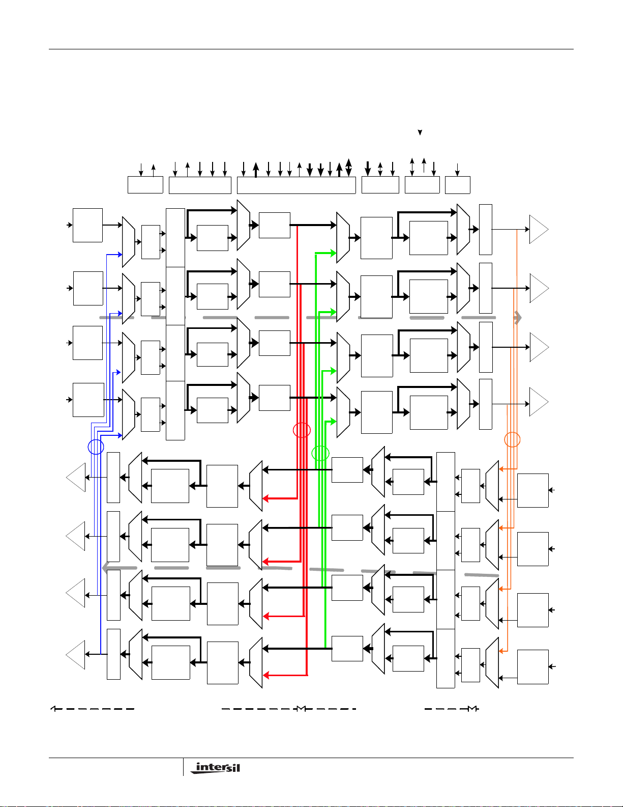
FIGURE 2. DETAILED FUNCTIONAL BLOCK DIAGRAM (BIST OMITTED)
(See also Figure 4 & Figure 5 for MDIO and LASI blocks and Figure 6 for BIST operation)
WRTP
SDC
RFC P/N
TXCK20
TDI
TDO
TMS
TCLK
TRSTN
LX4_MODE
RSTN
XP_ENA
MF[3:0]
TX_ENC
LASI
OPTxxx(3 pins)
GPIO[4:0]
TX_FAULT
TX_ENA[3:0]
OPRxxx(5 pins)
MDIO
PADR[4:0]
MDC
SDA
BIST_ENA
RXP0P/N
RXP1P/N
Egress
RXP2P/N
RXP3P/N
Loopback
TXP0 P/N
TXP1 P/N
Ingress
TXP2 P/N
TXP3 P/N
Equalizer
Signal
Detect
Equalizer
Signal
Detect
Equalizer
Signal
Detect
Equalizer
Signal
Detect
PHY XS
(Serial)
Serializer
Serializer
Serializer
Serializer
20X or 10X
Clock
CDR
CDR
CDR
CDR
Deserializer &
Deserializer &
Deserializer &
Deserializer &
8B/10B
Encoder,
AKR
Generator
8B/10B
Encoder,
AKR
Generator
8B/10B
Encoder,
AKR
Generator
8B/10B
Encoder,
AKR
Generator
Comma
Detector
Comma
Detector
Comma
Detector
Comma
Detector
10B/8B
Decoder
10B/8B
Decoder
10B/8B
Decoder
10B/8B
Decoder
TXFIFO &
Error and
Orderset
Detector
TXFIFO &
Error and
Orderset
Detector
TXFIFO &
Error and
Orderset
Detector
TXFIFO &
Error and
Orderset
Detector
MDIO Register, LASI & Common LogicJTAG
RX FIFO
Deskew
RX FIFO
Deskew
MDIO
Engine
TXFIFO &
Error and
Orderset
Detector
TXFIFO &
Error and
Orderset
Detector
I2C
8B/10B
Encoder,
Generator
8B/10B
Encoder,
Generator
BIST
AKR
AKR
LX4/CX4XAUI
Serializer
TCX0 P/N
Serializer
TCX1 P/N
Egress
CDR
CDR
CDR
CDR
S erializ er
TCX2 P/N
S erializ er
TCX3 P/N
PMA
Loop
back
Equalizer
Signal
Detect
Equalizer,
Signal
Detect
RCX0 P/N
RCX1 P/N
Ingress
Equalizer,
Signal
Detect
Equalizer,
Signal
Detect
RCX2 P/N
RCX3 P/N
RX FIFO
Deskew
RX FIFO
Deskew
PCS //
(PHY XS)
Loopback
TXFIFO &
Error and
Orderset
Detector
TXFIFO &
Error and
Orderset
Detector
PCS // Network
Loopback
RX FIFO
Deskew
RX FIFO
Deskew
RX FIFO
Deskew
RX FIFO
Deskew
10B/8B
Decoder
10B/8B
Decoder
10B/8B
Decoder
10B/8B
Decoder
8B/10B
Encoder,
AKR
Generator
8B/10B
Encoder,
AKR
Generator
Deserializer &
Detector
Comma
D es er ializ er &
Detector
Comma
Deserializer &
Detector
Comma
Deserializer &
Detector
Comma
Device Address 3 PCSDevice Address 4 PHY XGXS
8
Device Address 1 PMA/PMD

BBT3821
www.BDTIC.com/Intersil
General Description
The nLiten BBT3821 is a fully integrated octal 2.488Gbps to
3.1875Gbps Clock and Data Recovery (CDR) circuit and
Retimer ideal for high bandwidth serial electrical or optical
communications systems. It extracts timing information and
data from serial inputs at 2.488Gbps to 3.1875Gbps,
covering 10 Gigabit Fiber Channel (10GFC) and IEEE 802.3
specified 10 Gigabit Ethernet eXtended Attachment Unit
Interface (XAUI) rates.
Each BBT3821 accepts two sets of four high-speed
differential serial signals, re-times them with a local
Reference Clock, reduces jitter, and delivers eight clean
high-speed signals. The BBT3821 provides a full-function
XAUI-to-10GBASE-CX4 PMA/PMD (compatible with the
IEEE 802.3ak specification), and also can be configured to
provide the electrical portion of a XAUI-to-10GBASE-LX4
PMA/PMD, needing only laser drivers and photo detectors to
be added. In both these applications, the XAUI side can be
configured to implement the XENPAK MSA_R3.0
specification, including full NVR and DOM support. The
XPAK and X2 specifications currently all reference the
XENPAK specification, and are supported in exactly the
same manner. The BBT3821 can also be used to enhance a
single full-duplex 10 Gigabit XAUI link, extending the driving
distance of the high-speed (2.488Gbps to 3.1875Gbps)
differential traces to 40 inches of FR4 PCB (assuming a
proper impedance-controlled layout).
Each lane can operate independently with a data transfer
rate of within ±100ppm of either 20x or 10x the local
Reference Clock. The reference clock should be 156.25MHz
for 10 Gigabit Ethernet XAUI applications, and 159.375MHz
for 10 Gigabit Fiber Channel. Other reference frequencies
can be used for proprietary rates. For other applications,
each of the 8 lanes can be operated independently, within
the same data rate and clock restrictions.
The nLiten BBT3821 contains eight clock & data recovery
units, 8B/10B decoders and encoders, and elastic buffers
which provide the user with a simple interface for transferring
data serially and recovering it on the receive side. When
recovering an 8B/10B stream, a receive FIFO aligns all
incoming serial data to the local reference clock domain,
adding or removing IDLE sequences as required. This
simplifies implementation of an upstream ASIC by removing
the requirement to deal with multiple clock domains. The
Retimer can also be configured to operate as eight nonencoded 10-bit Retimers. Allowing long strings of
consecutive 1’s or 0’s (up to 512 bits), the nLiten BBT3821
has the capacity to accommodate proprietary encoded data
links at any data rate between 2.488Gbps and 3.1875Gbps
(and for half rate operation from 1.244Gbps to
1.59375Gbps).
The device configuration can be done through the use of the
two line Management Data Input/Output (MDIO) Interface
specified in IEEE 802.3 Clause 45. The BBT3821 supports a
5-bit Port Address, and DEVice ADdresses (DEVAD) 1, 3 & 4.
The initial values of the registers default to values controlled,
where appropriate, by external configuration pins, and set to
optimize the initial configuration for XAUI, CX4, and
XENPAK/XPAK/X2 use. Optionally, the BBT3821
configuration can be loaded at power-on or reset from the
NVR EEPROM or DOM used for the XENPAK/XPAK/X2
registers.
A full suite of loopback configurations is provided, including
the (802.3ae required) XAUI-transmit to XAUI-receive
loopback, and also the (802.3ae optional) PHY XGXS
loopback (effectively CX4/LX4-receive to CX4/LX4 transmit).
Lane-by-lane diagnostic loopback is available through
vendor-specific MDIO registers.
The low-power version BBT3821LP-JH is selected for
operation as an LX4 device at lowered supply voltages.
Functions
The nLiten BBT3821 serves three main functions:
• Pre-emphasize the output and equalize the input in order
to “re-open” the data eye, thus allowing CX4 operation,
and also increasing the available driving distance of the
high-speed traces in XAUI links.
• Clock compensation by insertion and deletion of IDLE
characters when 8B/10B encoding and decoding is
enabled.
• Automatic Byte and Lane Alignment, using both disparities
of /K/ for Byte alignment and either ||A|| or IDLE to DATA
transitions for lane alignment.
Receiver Operations
Loss of Signal Detection, Termination & Equalization
Each receiver lane detects and recovers the serial clock
from the received data stream. An equalizer has been added
to each receiver input buffer, which boosts high frequency
edge response. The boost factor can be selected from 16
values (none to full) through the MDIO Registers, (see
Table 43 for the PMA/PMD and Table 87 for the PHY XS).
A nominally 100Ω on-chip transmission line terminating
resistor is integrated with the input equalizer. This eliminates
the requirement of external termination resistors. It greatly
improves the effectiveness of the termination, providing the
best signal integrity possible.
There are also signal detect functions on each input lane,
whose “Loss Of Signal” (LOS) and “Signal Detect”
(SIG_DET) outputs appear in the MDIO Vendor-Specific
registers at address 1.C00A’h (Table 44) and 4.C00A’h
(Table 90). The LOS indication reflects the standard XAUI
specification, while the SIG_DET indication (CX4 inputs
only) implements the CX4 function. These signals can also
9

BBT3821
www.BDTIC.com/Intersil
be routed to the MF[3:0] pins (see Table 81 and Table 99).
The PMA configuration determines which of these signals
will be reflected in the IEEE PMD Receive signal detect
register at 1.10 (see Table 12), and contribute to the
RX_FAULT bit in the IEEE Status Register 2 at address 1.8
(see Table 10) and the LOCAL_FLT bit in the IEEE
PMA/PMD Status 1 Register, at address 1.1, (see Table 6).
The PHY XGXS LOS will be reflected in the IEEE Status
Registers at addresses 4.8 and 4.1 (see Table 77 and
Table 76). The threshold of the LOS detectors is controlled
via the 'LOS_TH' bits in the MDIO registers at 1.C001'h, see
Table 39, for the PMA/PMD, and for the PHY XS at
4.C001'h, see Table 81.
Clock and Data Recovery
When the 8B/10B coding is used, the line rate receive clock
is extracted from the transition rich 10-bit coded serial data
stream independently on each lane. When 8B/10B coding is
not used, longer run length (up to 512 1’s and 0’s) can be
supported. The data rate of the received serial bit stream
must be within ±100ppm of the nominal bit rate (strictly
within ±200 ppm of the multiplied local reference clock) to
guarantee proper reception. The receive clock locks to the
input within 2µs after a valid input data stream is applied.
The received data is de-serialized and byte aligned.
Byte Alignment (Code-Group Alignment)
Unless the CDET bits of the MDIO Registers at address
3.C000’h (for PCS, see Table 63) or 4.C000’h (for PHY XS,
see Table 80) are turned off, the respective Byte Alignment
Units are activated. Each Byte Alignment Unit searches the
coded incoming serial stream for a sequence defined in
IEEE 802.3-2002 Clause 36 as a “comma”. A comma is the
sequ ence “0011111” or “1100000” depending o n dis parity,
and is uniquely located in a valid 8B/10B coded data stream,
appearing as the start of some control symbols, including the
/K/ IDLE (K28.5). Comma disparity action can be controlled
via the same CDET bits of the registers [3:4].C000’h (see
Table 63 and Table 80). Any proprietary encoding scheme
used should either incorporate these codes, or arrange byte
alignment differently.
Upon detection of a comma, the Byte Alignment Unit shifts
the incoming data to align the received data properly in the
10-bit character field. Two possible algorithms may be used
for byte alignment. The default is that specified in the
IEEE802.3ae-2002 clause 48 specification, and is very
robust. This algorithm relies on the 10b/8b decoder, and
should not be used with proprietary encoding/decoding
schemes. The alternative is to byte-align on any comma
pattern. Although quick to align, and normally quite reliable,
this method is susceptible to realignment on certain single bit
errors or on successive K28.7 characters, but could be
preferable for proprietary coding schemes, or during debug.
The algorithm selection is controlled via MDIO register
PCS_SYNC_EN bits, for the PCS at address 3.C000’h
(Table 63), for the PHY XS at address 4.C000’h (Table 80),
unless overridden by the respective XAUI_EN bits in the
[3,4].C001’h registers (Table 64 and Table 81). Up to a full
code group may be deleted or modified while aligning the
“comma” code group correctly to the edges of the RefClock.
A comma received at any odd or even byte location, but at
the proper byte boundary, will not cause any byte realignment.
8b/10b Decoding
The internal 10b decoding specified in the IEEE802.3-2002
specification, section 36.2.4 in Tables 36-1 & 36-2, and
discussed in more detail in “8b/10b Coding and Decoding”
page 12, is enabled by default in the PCS and PHY XS
through the setting of the respective CODECENA bits to 1’b,
and may be disabled through the MDIO registers
[3,4].C000’h (Table 63 and Table 80) by setting the
respective bit to 0’b. Note that the transmit encoding will also
be disabled. Although Comma detection will still operate
normally, the PCS_SYNC engine (see above) may not
operate correctly on a proprietary coding scheme, unless
byte sync is performed on K28.5 characters, and no code
violations are to be expected in the proprietary data, and so
should normally be disabled if the 8b/10b coding is turned
off. The ‘fallback’ byte sync operations described above can
still be used, if the encoding scheme meets the “comma”
rules; otherwise they should be disabled also via the CDET
bits, and the user should expect unsynchronized 10-bit data
to be forwarded to the transmitter. No clock compensation is
then possible, and a synchronous reference clock should be
used throughout.
Receive FIFO
The Receive FIFO performs two functions:
1. Lane to Lane Alignment
2. Clock Compensation
Deskew (Lane to Lane) Alignment
Trunking, also known as deskewing, means the alignment of
packet data across multiple lanes. 8 bytes of RXFIFO are
dedicated for this lane to lane alignment in each direction.
During high-speed transmission, different active and passive
elements in the links may impart varying delays in the four
lanes. In trunking mode, multiple lanes share the same clock
(the local reference clock), which is used to transfer data for
output on the serial transmitter.
Deskewing is accomplished by monitoring the contents of
the FIFOs to detect either an /A/ code-group on every lane
(an ||A|| Ordered_Set), or the boundary between IDLE
sequences and any non-IDLE data (see Table 1); the latter
boundary defines the beginning of the packet. The choice of
which alignment markers to use can be controlled by the
A_ALIGN_DIS bits in MDIO [3,4].C000’h (see for PCS
Table 63 and for PHY XS Table 80), unless overridden by
the respective XAUI_EN bits in the [3,4].C001’h registers
(Table 64 and Table 81) to align on ||A||. When this alignment
10
BBT3821
www.BDTIC.com/Intersil
data is detected in all four lanes within the span of the
Alignment FIFO, the deskewing (lane to lane) alignment
operation is performed, and will be held until another ||A|| or
IDLE-to- non-IDLE transition is detected again on the lanes.
During this alignment, up to four code groups may be
deleted on any lane. For correct operation, the XAUI Lane 0
signals should be connected to the BBT3821 Lane 0 pins.
The deskew algorithm state machines (each implemented
according to IEEE 802.3ae) are enabled by setting the
DSKW_SM_EN bits (Address [3,4].C000’h, see Table 63
and/or Table 80) to 1 or overriding them with the respective
XAUI_EN bits in the [3,4].C001’h registers (Table 64 and
Table 81). Note that when one side’s DSKW_SM_EN is set
to 1, the same side CAL_EN bit (Address [3,4].C000’h,
Table 63/Table 80) is ignored. When a DSKW_SM_EN bit is
set to 0, lane deskew can still be enabled by setting
CAL_EN, but the deskew action will be carried out without
hysteresis.
The user has the option to disable trunking, or to enable
trunking across each set of 4 lanes, in the PCS (device 3)
and PHY XGXS (device 4), under control of the respective
PSYNC bits in registers [3,4].C000h. In trunking mode, the
lanes may have phase differences, but they are expected to
be frequency synchronous. In non-trunking mode, each
received serial stream need only be within ±100ppm of the
nominal bit rate (2.488Gbps to 3.1875Gbps in full-speed
mode or 1.244Gbps to 1.59375Gbps in half-speed mode).
Setting the PSYNC bits high will enable the trunking mode,
so that all transmitted data will be synchronized to the same
clock. Note that trunking mode is only possible if 8B/10B
Coding is activated, and all lanes have the same half-rate
setting (See Table 71).
Clock Compensation
In addition to deskew, the Receive FIFOs also compensate
for clock differences. Since the received serial streams can,
under worst case conditions, be off by up to ±200ppm from
the local clock domain, the received data must be adjusted
to the local reference clock frequency.
Another 8 bytes of RXFIFO are dedicated for clock
compensation. The FIFOs achieve clock tolerance by
identifying any of the IDLE patterns (/K/, /A/ or /R/ as defined
by the IEEE 802.3ae standard) in the received data and then
adding or dropping IDLEs as needed. The Receive FIFO
does not store the actual IDLE sequences received but
generates the number of IDLEs needed to compensate for
clock tolerance differences. The IDLE patterns retransmitted
will be determined according to the IEEE 802.3ae algorithm
if the appropriate AKR_SM_EN bit is set in Registers
[3,4].C001’h (see Table 64 and Table 81).
Transmitter Operations
8b/10b Encoding
The internal 10b encoding specified in the IEEE802.3-2002
specification, section 36.2.4 in Tables 36-1 & 36-2, and
discussed in more detail in “8b/10b Coding and Decoding”
page 12, is enabled by default in the PCS and PHY XS
through the setting of the respective CODECENA bits to 1’b,
and may be disabled through the MDIO registers
[3,4].C000’h (see Table 63 and Table 80) by setting the
respective bit to 0’b. Note that the receive decoding will also
be disabled. The (decoded, synchronized and aligned) data
is transferred via the transmit FIFOs, (normally) encoded,
serialized and re-transmitted on the Serial Output pins,
whose effective output impedance is nominally 100Ω
differential.
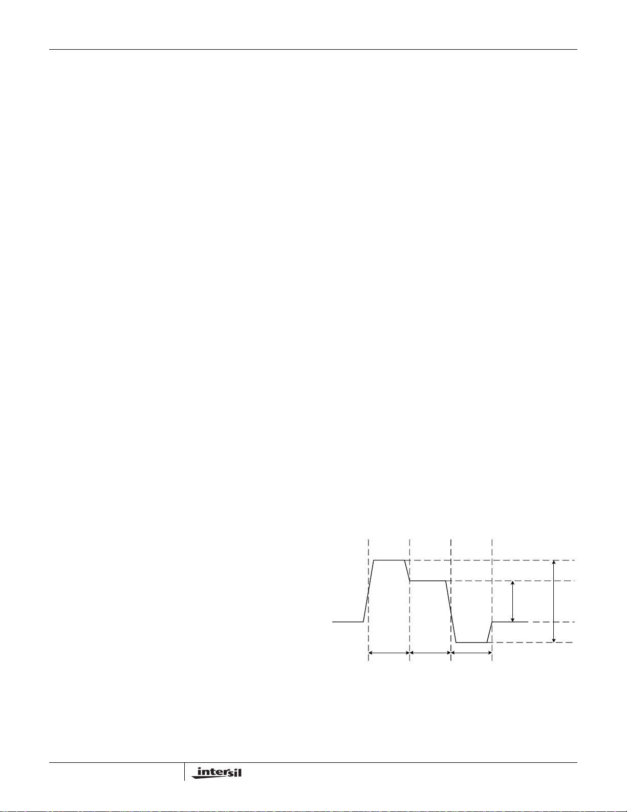
Pre-Emphasis
In order to compensate for the loss of the high frequency
signal component through PCB traces or the CX4 Cable
Assembly, sixteen levels of programmable pre-emphasis
have been provided on the CX4/LX4 PMA serial transmit
lanes, and eight levels on the XAUI PHY XS serial transmit
lanes. The output signal is boosted immediately after any
transition (see Figure 3). This maximizes the data eye
opening at the receiver inputs and enhances the bit error
rate performance of the system. The MDIO Registers at
Addresses [1,4].C005’h (see Table 41 and Table 85) control
the level of pre-emphasis for the PMA/PMD (sixteen levels)
and PHY XGXS (eight levels) respectively, settable from
none to the maximum. The initial default values of the
PMA/PMD register depend on the LX4_MODE configuration
pin, and are set to the optimum values for CX4 or XAUI
(assumed best for LX4 drivers). Both these registers may be
auto-loaded (see Auto-Configuring Control Registers
page 16) from an NVR EEPROM on start-up or RESET.
FIGURE 3. PRE-EMPHASIS OUTPUT ILLUSTRATION
1
Bit
Time
1
Bit
Time
00
V
LOW-pp
Bit
Time
V
HI-pp
11

BBT3821
www.BDTIC.com/Intersil
8b/10b Coding and Decoding
another column containing a non-idle is received. If in
addition either of the AKR_SM_EN or XAUI_EN bits in the
8 Bit Mode
If 8B/10B encoding/decoding is turned on, the nLiten
BBT3821 expects to receive a properly encoded serial bit
stream. The serial bit stream must be ordered “abcdeifghj”
with “a” being the first bit received and “j” the last. If the
received data contains an error, the Retimer will re-transmit it
as an ERROR or /E/ character. The character transmitted
may be controlled via the ERROR code Registers
[3,4].C002’h, Table 66 and Table 82. The internal decoding
into, and encoding from, the FIFOs is listed in Table 1 below.
If the TRANS_EN bit or XAUI_EN bit (MDIO Registers at
addresses [3,4].C001’h, see Table 64 and Table 81 are set,
all incoming XAUI or CX4/LX4 IDLE patterns will be
converted to the (internal) XGMII IDLE pattern set by the
respective PCS or PHY XS control registers at addresses
[3,4].C003’h, with a default value 107’h, the standard XGMII
IDLE code (see Table 67 and Table 83) in the internal FIFOs.
The first full column of IDLES after any column containing a
non-IDLE will be stored in the respective elasticity FIFO, and
all subsequent full IDLE columns will repeat this pattern, until
Table 1. VALID 10b/8b DECODER & ENCODER PATTERNS
RECEIVING SERDES INTERNAL DATA TRANSMITTING SERDES NOTES
SERIAL CODE,
CHARACTER
Valid Data X 0 0 0-FF’h X See 802.3
/K/ (Sync) K28.5 1 0 1 07’h
/A/ (Align) K28.3 1 0 1 07’h
/R/ (Skip) K28.0 1 0 1 07’h
/S/ K27.7 X 0 1 FB 1 /S/ K27.7 Start
/T/ K29.7 X 0 1 FD 0 /T/ K29.7 Terminate
K28.1 X 0 1 3C X K28.1 Extra comma
/F/ K28.2 X 0 1 5C X /F/ K28.2 Signal Ordered_Set
/Q/ K28.4 X 0 1 9C X /Q/ K28.4 Sequence Ordered_Set
K28.6 X 0 1 DC X K28.6
K28.7 X 0 1 FC X K28.7 Repeat has False Comma
K23.7 X 0 1 F7 X K23.7
/E/ K30.7 X 1 1 FE X /E/ K30.7 Error Code
Any other X 1 = ERROR reg.
Note (1): First incoming IDLE only, subsequent IDLEs in that block repeat first received code.
Note (2): Default value, actually set by ‘Internal Idle’ register, [3:4].C003’h, see Table 67 and Table 83.
Note (3): Value set by ‘ERROR Code’ register, [3:4].C002’h, see Table 66 and Table66. The XAUI_EN bit forces it to 1FE’h.
Note (4): If the XAUI_EN bit is set, the BBT3821 acts as though both the TRANS_EN and AKR_EN bits are set.
TRANS_EN
(4)
BIT
001BC
0017C
0011C
E-BIT K-BIT
INTERNAL
FIFO DATA
AKR_SM_
(2)
(1)
(2)
(1)
(2)
(1)
(3)
respective MDIO registers at Addresses [3,4].C001’h is set
(see Table 64 and Table 81, these IDLEs will be sequenced
on transmission into a pseudo-random pattern of ||A||, ||K||,
and ||R|| codes according to the IEEE 802.3ae specified
algorithm. If neither of the AKR_SM_EN and XAUI_EN bits
are set, the internal IDLEs will all be transmitted as /K/
codes. Elasticity will be achieved by adding or deleting
columns of internal IDLEs.
If neither the TRANS_EN bit nor the XAUI_EN bit is set (for
either the PCS or the PHY XS), the incoming XAUI IDLE
codes will all be decoded to the appropriate XGMII control
code values in the respective internal FIFO. If the AKR_EN
or XAUI_EN bits are set, they will be sequenced into a
pseudo-random pattern of ||A||, ||K||, and ||R|| codes and
retransmitted, if not, the Inter Packet Gap (IPG) will be
retransmitted as the same XAUI codes as in the first full
IDLE column.
For most applications, the XAUI_EN bit high configuration is
the most desirable, and is the default.
(4)
EN
1 /A/ /K/ /R/ IEEE802.3ae algorithm
0 /K/ K28.5 Comma (Sync)
1 /A/ /K/ /R/ IEEE802.3ae algorithm
0 /A/ K28.3 Align
1 /A/ /K/ /R/ IEEE802.3ae algorithm
0 /R/ K28.0 Alternate Idle (Skip)
X Invalid code Error Code
SERIAL
CHARACTER
Table
SERIAL
CODE DESCRIPTION
Valid Data Same Data Value as Received
12

BBT3821
www.BDTIC.com/Intersil
10 Bit Mode
If a PCS or PHY XS 8B/10B codec is inactive (the respective
XAUI_EN AND CODECENA bits are disabled, see
Table 63/Table 64 & Table 80/Table 81), no 8b/10b coding or
decoding is performed. The incoming bits will be arbitrarily split
into 10 bit bundles in the internal FIFO, optionally based on any
commas received, but otherwise not checked, and must be
retransmitted in the same clock domain, since no elasticity is
possible. Therefore the local reference clock must be frequency
synchronous with the data source. Only the jitter domain will be
reset. System designers must ensure that the data stream is
adequately DC-balanced and contains sufficient transition
density for proper operation, including synchronization.
Error Indications
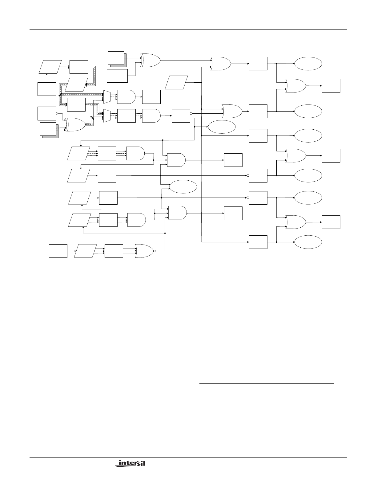
An equivalent schematic of the various IEEE-defined and
Vendor Specific Fault and Status registers in the BBT3821 is
shown in Figure 4. Those register signals that also contribute to
the LASI system are indicated (see Figure 5).
Loss of Signal
If the reference clock is missing or at an out-of-range frequency,
the PLL in the CMU will fail to lock. This is the only possible
internal cause of a PMA ‘TX Local Fault ‘ indication in bit 1.8.11
(Table 10), and will cause ‘RX Local Fault’ in bit 1.8.10 and
other consequent fault indications (see Table 6, Table 27 and
Table 28).
Loss of the input signal may be caused by poor connections,
insufficient voltage swings, or excessive channel loss. If any of
these conditions occurs, the Loss Of Signal (LOS) and (CX4)
SIG_DET detector outputs on the lane will indicate the fault,
and may be monitored via the MDIO system (see Table 6,
Table 10, Table 27, Table 28, Table 76 and Table 77). See also
the section on “Loss of Signal Detection, Termination &
Equalization“ on page 9 above. In addition, the MDIO MF_SEL
and MF_CTRL register bits (address 4.C001’h, see Table 81)
may be set to provide the LOS/SIG_DET indication on the
MF[3:0] pins.
Channel Fault Indications
Any of the above faults (LOS/SIG_DET, Byte Sync, or Lane
Align), will (by default) cause a local fault in the relevant
receiver. If the PCS_SYNC_EN bit at address [3,4]C000’h (or
the XAUI_EN bit at [3:4].C001’h) (see Table 63 to
Table 65 and/or Table 80 to Table 81) is set, the internal FIFOs
will propagate the local fault indication specified in the
IEEE802.3ae-2002 specification (Sections 46.3.4 and 48.2.4.2)
as the Sequence Ordered_Set ||LF|| (see Table 48-4),
/K28.4/D0.0/D0.0/D1.0/, which will be transmitted as the
appropriate XAUI or LX4/CX4 TX output. The BBT3821 lanes
0-3 must be connected to XAUI and LX4/CX4 lanes 0-3 in strict
order. Any Sequence Ordered_Set (including ||LF|| and ||RF||)
received on an input channel will be retransmitted unchanged
on the appropriate output channel.
Coding Violation, Disparity & FIFO Errors
The 8b/10b decoder will detect any code violation, and replace
the invalid character by the error character /E/. In the case of a
disparity error, the error may be propagated and only flagged at
the end of a packet (according to the IEEE 802.3 rules). The
BBT3821 will handle this according to those rules. In addition,
the MDIO system includes a flag, in registers [3,4].C007’h on
bits 11:8 (see Table 69 and Table 88). Similarly, an error in the
PCS or PHY XS Elastic (clock compensation) FIFOs will be
flagged in bits 7:4 of the same registers. The FIFO errors may
also be flagged on the MF[3:0] pins via the MDIO MF_SEL and
MF_CTRL register bits (address 4.C001’h, see Table 81).
If a PCS or PHY XS 8B/10B codec is inactive, disparity error
and coding violation errors do not apply, and the FIFOs have no
active error source.
Loopback Modes
In addition to the IEEE 802.3ae-required loopback modes,
the BBT3821 provides a number of additional modes. Each
mode is described in detail below, by reference to the
Detailed Functional Block Diagram in Figure 2, together with
the register bits controlling it.
Byte or Lane Synchronization Failure
The MDIO system can indicate a failure to achieve Byte
Synchronization on any lane, in the PCS register bits 3.24.3:0
(Table 61) or in the PHY XS register bits 4.24.3:0 (Table 78),
which shows the lane-by-lane Byte Sync status. A failure here,
if not caused by any of the above ‘Loss of Signal’ conditions,
would normally reflect a very high bit error rate, or incorrectly
coded data.
Failure of Lane Synchronization is indicated for the PCS by
register bit 3.24.12 (Table 61) or for the PHY XS by register bit
4.24.12 (Table 78), and can be caused by failure to detect /A/
characters on every lane of a channel, by excessive skew
between /A/s on the lanes of a channel, or by inconsistent
skews.
13
PMA Loopback (1.0.0 & 1.C004.[11:8])
The PMA loopback is implemented from the output of the
TCX[3:0] serializers to the input multiplexers in front of the
RCX[3:0] CDRs. All four lanes are controlled by bit 1.0.0,
while the individual lanes can be controlled (one at a time)
by the 1.C004’h.[11:8] bits. Assuming that this is the only
loopback enabled, and that the BIST and test pattern
generation features are not enabled, the signal flow is from
the RXP[3:0][P/N] pins through almost all the ‘egress’
channel to the input of the (still active) TCX[3:0] output
drivers, then (bypassing the RCX[3:0][P/N] inputs, the
equalizers and LOS detectors) back from the CDRs through
almost all the ‘ingress’ channel to the TXP[3:0][P/N] pins.
BBT3821
www.BDTIC.com/Intersil
FIGURE 4. IEEE AND VENDOR SPECIFIC FAULT AND STATUS REGISTERS (EQUIVALENT SCHEMATIC)
PMA/PMD
SIGNAL
DETECT
level
REG
1.C001.10:8
REG
1.C01D.6
OPRLOS
[3:0]
REG
1.C00A.3:0
CX4
SIGNAL_
DETECT
REG
1.C00A.7:4
PCS
BYTE
SYNC
PCS
LANE
ALIGN
PHY XS
LANE
ALIGN
PHY XS
BYTE
SYNC
TXFAULT
IEEE REG
1.10.4:1
PLL LOCK
FAIL
IEEE REG
1.1.2
IEEE REG
1.10.0
See LASI
IEEE REG
3.1.2
See LASI
IEEE REG
4.1.2
POLARITY
CX4
LX4
CX4
LX4
IEEE REG
3.24.3:0
IEEE REG
3.24.12
IEEE REG
4.24.12
IEEE REG
4.24.3:0
REG
1.C012h.13
IEEE REG
1.8.11
IEEE REG
1.8.10
IEEE REG
3.8.11
IEEE REG
3.8.10
IEEE REG
4.8.11
See LASI
See LASI
See LASI
See LASI
See LASI
IEEE REG
1.1.7
IEEE REG
3.1.7
IEEE REG
4.1.7
REG
3.C001.10:8
level
PHY XS
SIGNAL
DETECT
REG
4.C00A.3:0
PHY XS (Serial) Loopback (4.0.14 & 4.C004.[11:8])
The PHY XS loopback is implemented from the output of the
TXP[3:0] serializers to the input multiplexers in front of the
RXP[3:0] CDRs. All four lanes are controlled by bit 4.0.14,
while the individual lanes can be controlled (one at a time) by
the 4.C004’h.[11:8] bits. Assuming that this is the only
loopback enabled, and that the BIST and test pattern
generation features are not enabled, the signal flow is from
the RCX[3:0][P/N] pins through almost all the ‘ingress’
channel to the input of the (still active) TXP[3:0] output drivers,
then (bypassing the RXP[3:0][P/N] inputs, the equalizers and
LOS detectors) back from the CDRs through almost all the
‘egress’ channel to the TCX[3:0][P/N] pins.
PCS Parallel Network Loopback (3.C004.[3:0])
This loopback is implemented (at the internal XGMII-like level)
from the output of the RXFIFOs in the ‘ingress’ channel to the
input of the TXFIFOs in the ‘egress’ channel. The individual
lanes can be controlled (one at a time) by the 3.C004’h.[3:0]
bits. Assuming that this is the only loopback enabled, and that
the BIST and test pattern generation features are not enabled,
the signal flow is from the RCX[3:0][P/N] pins through the
PMA/PMD and PCS and again PMA/PMD to the
TCX[3:0][P/N] pins. This could also be seen as a ‘short’
loopback at the XGMII input of the PHY XS.
IEEE REG
4.8.10
See LASI
PCS (Parallel) Loopback (4.C004.[3:0] & Optionally
3.0.14)
This loopback is implemented (at the internal XGMII-like level)
from the output of the RXFIFOs in the ‘egress’ channel to the
input of the TXFIFOs in the ‘ingress’ channel. The individual
lanes can be controlled (one at a time) by the 4.C004’h.[3:0]
bits. If the enable bit in 3.C001.7 (Table 64) is set, all four
lanes can be controlled by bit 3.0.14. Since the latter is
specifically excluded by subclause 45.2.3.1.2 of the IEEE
802.3ae-2002 specification for a 10GBASE-X PCS, the
default is to NOT enable this loopback bit, and if it is enabled,
the BBT3821 does not conform to the IEEE specification. A
maintenance request has been submitted to the IEEE to
enable this loopback bit as optional, and to allow a ‘PCS
Loopback Capability’ bit in register bit 3.24.10 (see
http://www.ieee802.org/3/maint/requests/maint_1113.pdf
this has so far been rejected, and may never be approved.
Assuming that this is the only loopback enabled, and that the
BIST and test pattern generation features are not enabled, the
signal flow is from the RXP[3:0][P/N] pins through the full PHY
XS via the internal XGMII to the TXP[3:0][P/N] pins. This
could also be seen as a ‘short’ loopback at the XGMII input of
the PCS.
), but
14
BBT3821
www.BDTIC.com/Intersil
Serial Test Loopbacks (1.C004.12 & 4.C004.12)
In addition to the above loopbacks, the BBT3821 also offers
two serial loopbacks directly between the serial inputs and
outputs. These loopbacks use the recovered clock as the
timing for the outputs (instead of the multiplied reference
clock), so do not reset the jitter or clock domains, and in
addition do NOT provide any pre-emphasis on the outputs.
Furthermore, on the PMA/PMD side (1.C004.12) the lanes
are internally swapped (so the Lane 3 output is from the
Lane 0 input, etc.). Because of their limited utility, they are
not illustrated in Figure 2 or Figure 6. They are mainly useful
for debugging an otherwise intractable system problem. The
reference clock still needs to be within locking range of the
input frequency. The remainder of the signal path will remain
active (as normal), so that if for example 1.C004.12 is set,
data coming in on RCX[3:0], in addition to emerging on
TCX[0:3] without retiming, etc., will also emerge from
TXP[3:0] retimed, as usual.
Serial Management Interface
The nLiten BBT3821 implements the MMD Management
Interface defined in IEEE 802.3-2002 Clauses 22 &
enhanced in IEEE 802.3ae-2002 Clause 45. This two-pin
interface allows serial read/write of the internal control
registers and consists of the MDC clock and MDIO data
terminals. The PADR[4..0] pins are used to select the ‘Port
address’ to which a given nLiten BBT3821 device responds.
The BBT3821 will ignore Clause 22 format frames (on a
frame-by-frame basis), based on the second ST (start) bit
value. The two formats are shown in Table 3, together with
the references to the respective IEEE 802.3 specifications.
MDIO Register Addressing
The PADR[4..0] hardware address pins control the PRTAD
(Port Address) value, each port normally consisting of a
series of MDIO Managed Devices (MMDs). Each Port may
include up to 31 different devices, of which the current
specification defines 8 types, and allows vendor
specification of two others. The BBT3821 device
corresponds to the PMA/PMD, PCS and PHY XGXS defined
types, so responds to DEVAD values of 1, 3 and 4
respectively. The Clause 45-accessible registers are listed
for each Device Address in the tables referenced in Table 2.
Many of these register addresses are IEEE-defined; the
‘Vendor Defined’ registers are arranged to be as DEVAD
independent as possible.
Table 2. DEVAD DEVICE ADDRESS TABLE
REGISTER LIST
DEVAD VALUE IEEE DEFINITION
DEVAD = 1 (00001’b) PMA/PMD Device Table 4, page 19
DEVAD = 3 (00011’b) PCS Device Table 56, page 38
DEVAD = 4 (00100’b) PHY XS (XGXS)
Each individual device may have up to 2
registers. The BBT3821 implements all the defined registers
for 10GBASE PMA/PMD, 10GBASE-X PCS and PHY XS
devices, and a few Vendor Specific registers for each
DEVAD respectively. The latter have been placed in the
blocks beginning at D.C000’h so as to avoid the areas
currently defined as for use by the XENPAK module and
similar MSA devices, to facilitate use of the BBT3821 in such
modules and systems.
Device Table 74, page 45
16
TABLE
(65,536)
Table 3. MDIO MANAGEMENT FRAME FORMATS
CLAUSE 22 FORMAT (FROM TABLE 22-10 IN IEEE STD 802.3-2002 EDITION, FOR REFERENCE)
OPERN PRE ST OP PHYAD REGAD TA DATA IDLE
Read 1….1 01 10 PPPPP RRRRR Z0 DDDDDDDDDDDDDDDD Z
Write 1….1 01 01 PPPPP RRRRR 10 DDDDDDDDDDDDDDDD Z
CLAUSE 45 FORMAT (FROM TABLE 45-64 IN IEEE 802.3.ae-2002)
(1)
OPERN PRE
Addrs 1….1 00 00 PPPPP DDDDD 10 AAAAAAAAAAAAAAAA Z
Write 1….1 00 01 PPPPP DDDDD 10 DDDDDDDDDDDDDDDD Z
Read 1….1 00 11 PPPPP DDDDD Z0 DDDDDDDDDDDDDDDD Z
Read Inc 1….1 00 10 PPPPP DDDDD Z0 DDDDDDDDDDDDDDDD Z
Note (1): The ‘Preamble’ consists of at least 32 bits. After a software reset, a few extra preamble bits may be needed, depending on the MDC clock rate. See timing
diagrams in Figure 15 and Figure 17.
Note (2): The actual register will not be updated until up to three additional MDC cycles have been received. See Figure 15.
ST OP PRTAD DEVAD TA ADDRESS/DATA IDLE
(2)
15

BBT3821
www.BDTIC.com/Intersil
I2C Space Interface
In addition to the standard MDIO registers discussed above,
the BBT3821 implements the register addresses specified in
the XENPAK MSA specification for the NVR, DOM and LASI
blocks. The built-in I
these registers with the MSA-specified data on start-up or
reset or on demand from an I
included as part of a DOM circuit) and/or one or four DOM
circuits (see below). Optionally, a portion of the NVR space
may be used to autoload the various BBT3821 control
registers at start-up or reset. These operations are
discussed in more detail below.
NVR Registers & EEPROM
If the XP_ENA pin is asserted enabled (high), at the end of
hardware RESET or power-up the BBT3821 will attempt to
load the NVR area by initiating a NVR-block read through
the 1.32768 (1.8000’h) control register (Table 15). See
Figure 18. The same will occur if the appropriate command
value is written into this register. The I
attempt to read the A0.00:FF’h I
1.8007:8106’h MDIO register space. The Command Status
bits in the 1.32768 (1.8000’h) Control register will reflect the
status of this operation. Failure may occur if the expected
ACK is not received from any address after the number of
attempts set in control register 1.32273 (1.8005’h), default
63 (Table 20), or if a collision is detected on the I
timing sequence of this Block Read operation is shown in
Figure 20. The host can check the checksums against the
values at 1.807D, and optionally 1.80AD and 1.8106, and
take appropriate action. As soon as the XENPAK MDIO
space is loaded, the STA MDIO device may interrogate it.
Note that the BBT3821 merely stores the values read from
the EEPROM or other device at A0.00-FF’h, and, with a few
exceptions, does not interpret them in any way. The
exceptions are listed explicitly in Table 22, together with the
other uninterpreted groups, and are:
• The Package OUI at 1.32818:32821 (1.8032:5’h), which
will be mirrored in the IEEE-defined 1.14:15 (1.E:F’h)
space, as required by section 10.8.2 of the XENPAK spec;
the allowable values here are specified by the XENPAK,
XPAK and X2 specifications;
• The DOM Capability byte at 1.32890 (1.807A), see the
DOM Registers section, page 16;
• The Auto-configure size and pointer bytes at
1.33028:9(1.8104:5); (see Auto-Configuring Control
Registers, page 16).
• If the Auto-configure operation is enabled, the block of
bytes so specified will be written into the BBT3821 control
registers, (see Auto-Configuring Control Registers on
page 16 and Table 92).
Other registers may be interpreted in future versions of the
BBT3821.
2
C controller can be configured to load
2
C EEPROM (frequently
2
C interface will
2
C space into the
2
C bus. The
Auto-Configuring Control Registers
If the XP_ENA pin is asserted, and the I2C controller can
successfully read the I
space, the BBT3821 will examine the Auto-configure Pointer
value at 1.33029 (1.8105’h). If this is neither 00’h or FF’h,
the BBT3821 will use that value (S below) as an offset
pointer into the A0.00:FF’h I
MDIO NVR space, and the number of bytes given in the
Auto-configure Size register 1.33028 (1.8104) value (N
below) to load N bytes from the NVR data starting from
location S into the various BBT3821 configuration control
registers. The loading sequence and the correspondence
between the NVR block and the control registers is listed in
Table 92. The auto-configure engine will behave benignly if
the S and N values are misconfigured, so that if S + N ≥ 252
(for example), the auto-configure block will stop at an S + N
value of 252, and not use S, N , or the Checksum value to
load a configuration control register. (Hence the exclusion of
FF’h as a value for S is no limitation). Similarly, values of N >
40 will be ignored.
Note that in a XENPAK/XPAK/X2 module, the value of S should
not be between 00’h and 76’h, since this would start the loading
from within the MSA-defined region. (Hence the exclusion of
00’h as a value for S is normally no limitation). If the value of S
lies between 77’h and A6’h, that portion of the auto-configure
data within that band can be overwritten as part of the
Customer Writable area defined by the MSA specifications; if
this is undesirable, that range of values should also be
excluded. On the other hand, this could be used to allow some
customization for specific end-user configuration values. If the
block overlaps the boundary between the ‘Customer Writable’
and ‘Vendor Specific’ areas, the first part would be customerwritable, and the second part not. The order of the configuration
registers has been arranged to place those most likely to be
useful in such a customer-configuration environment at the
beginning of the block. The ‘Customer Area Checksum’ would
be part of the auto-configure block, and some other byte in the
‘Customer Writeable Area’ would need to be adjusted to make
the Checksum and the desired configuration value coincide.
The Command Status bits in the NVR Command register
(Table 15) at 1.32768.3:2 (1.8000’h.3:2) will reflect the success
of both the NVR and (if called for) the auto-configure loading
operations.
2
C NVR space into the MDIO NVR
2
C space already copied into the
DOM Registers
If the NVR load operation succeeds, the (newly read-in)
XENPAK register at 1.32890 (1.807A’h) is examined, and if the
DOM Capability bit is set (bit 6, see Table 23), the I
will attempt to read the DOM values from the I
address space specified in the same register (bits 2:0),
normally 001’b pointing to A2’h. See Note (2) to Table 23 for
details. A full block of data will be read from this space (normally
A2.00:FF’h) into the 1.40960:41215 (1.A000: A0FF’h) MDIO
register DOM space. See Figure 18 and Figure 20 for details.
The DOM control register is implemented in the BBT3821 at
2
C interface
2
C device
16

BBT3821
www.BDTIC.com/Intersil
1.41216 (1.A100’h), so that one-time or (by default) periodic
updates of the DOM information can be loaded into the MDIO
DOM space by writing the appropriate values into it, as shown
in Table 38, page 33. The actual automatic update rates
selectable in this XENPAK-defined register are controlled by
the DOM Control register in the BBT3821 vendor-specific
register space at 1.49176 (1.C018’h), which also controls other
actions of the DOM interface (see Table 51). In particular, since
many available DOM circuits can handle only one lane, bit 2
enables or disables indirect access to separate DOM circuits on
the four lanes. If the bit is 0’b, the DOM circuit is directly
addressed at Ax.00:FF’h, and is assumed to provide the full
four lane data, including the determination of which data is to be
treated as the ‘furthest out of range’ or the ‘representative
value’, as specified in Note 1 to Table 27 in section 11.2.6 of the
XENPAK R3.0 specification, to be returned in the XENPAKdefined 1.A060:A06D’h space for a WDM module. If bit 2 of
1.C018’h is set to 1’b, the DOM data is polled from four devices
attached to the I
them. The 40 bytes of data are stored in the four lane register
blocks starting from 1.A0C0’h, 1.A0D0’h, 1.A0E0’h and
1.A0F0’h respectively. The device addresses of these four
DOM devices on the 2-wire bus are configured by registers
1.C01B’h and 1.C01C’h (Table 54); the starting memory
addresses by registers 1.C019’h and 1.C01A’h (Table 53).
Since the BBT3821 has no mechanism to determine out-ofrange data, it chooses one of these four 10-byte long groups of
data to copy into 1.A060’h:A069’h according to bits 1:0 of
1.C018’h (the ‘representative’ lane per the above-mentioned
XENPAK Note). In addition, the Alarm and Status flags
(Table 36 and Table 37) will be loaded from this lane into
1.A070:A075’h.
The BBT3821 assumes that the DOM circuit(s) will have
these A/D values and flags at the same relative offsets as
those specified in the XENPAK R3.0 and the SFF-8472
specifications.
2
C serial bus, getting 10 bytes from each of
General Purpose (GPIO) Pins
The BBT3821 includes some flexibly configurable General
Purpose Input-Output (GPIO) pins, which may be configured
to be inputs or outputs. As inputs, their level may be read
directly via the MDIO system, but also they may be
configured (again via MDIO registers, see Table 47 through
Table 50) to optionally trigger the LASI on either a high or
low level. The GPIO pins may also individually be used as
outputs, and set high or low, under MDIO control. The GPIO
control registers are among those that can be autoconfigured on start-up.
LASI Registers & I/O
The BBT3821 implements the Link Alarm Status Interrupt
(LASI) interface defined in section 10.13 of the XENPAK
specification. The source and nature of these is described
above under “Error Indications” on page 13 and in Figure 4.
In addition to these specification-defined inputs, the
BBT3821 incorporates a number of additional inputs, related
to the possible byte alignment and 8b/10b code violations,
which may be used to trigger a LASI. The available inputs
depend on the LX4/CX4 select LX4_MODE pin (Table 99),
and are detailed in Table 27 and Table 28, and include:
1. Various status bits within the BBT3821, derived from its
operations; in particular, the LOS indications, Byte Sync
and EFIFO errors, the Fault bits [1,3,4].8.10:11, etc.
2. The Optical Interface Status pins (in LX4 mode), see
Table 99.
3. The Alarm flags in 1.A070:1 (Table 36). These bits
are gated with the enable bits in 1.9006:7 (Table 30 and
Table 31) and the LX4/CX4 LX4_MODE pin (Table 99) to
drive bits 1.9004.1 & 1.9003.1 (Table 28 & Table 27).
4. The GPIO pins (Table 100). If configured as inputs, they
may be used to optionally trigger the LASI on either a
high or low level. See above.
These status inputs can all be read via the LASI Status
registers (1.9003 to 1.9005, see Table 27 to Table 29). Any of
these inputs, if enabled via the LASI Control Registers, 1.9000
to 1.9002 (Table 24 to Table 26), can drive the LASI pin.
Figure 5 shows an equivalent schematic for the LASI system
(an expansion of Figure 21 in the XENPAK specification).
Reading Additional EEPROM Space Via the I2C Interface
The I2C interface will allow single-byte reads from any
possible I
address are written into the 1.32769 (1.8001’h) and
1.32770 (1.8002’h) registers respectively (see Table 16 and
Table 17), and on issuing a ‘Read one byte’ command (write
0002’h to 1.32768 = 1.8000’h) the data will be read from the
2
I
C space in the MDIO register at 1.32771 (1.8003’h, see
Table 18). For timing sequence, see Figure 22. Note that a
16-bit addressable EEPROM (or equivalent) device on the
2
I
C bus may be read by setting the Long Memory bit
1.32773.8 (1.8005.8’h) to a ‘1’, and writing a full 16-bit
memory address value into 1.32770 (1.8002’h). This in
principle allows access to almost a full 8MB of I
excluding only the NVR and (optional) DOM device address
portions. This 16-bit operation MUST NOT be used on an
8-bit device, since the register address setting operation will
attempt to write the low byte of the address into the register
at the high byte address. Such a 16-bit memory address
device should be located at a device address not used by
the NVR or DOM system.
These one-byte operations could be used to read other
types of data from (multiple) DOM devices (such as limit
lookup tables), or for expanded informational areas. It also
facilitates the use of I
Potentiometer) devices for Laser Current control, and other
similar setup and monitoring uses.
2
C address. The device address and memory
2
C space,
2
C-based DCP (Digital Control
17
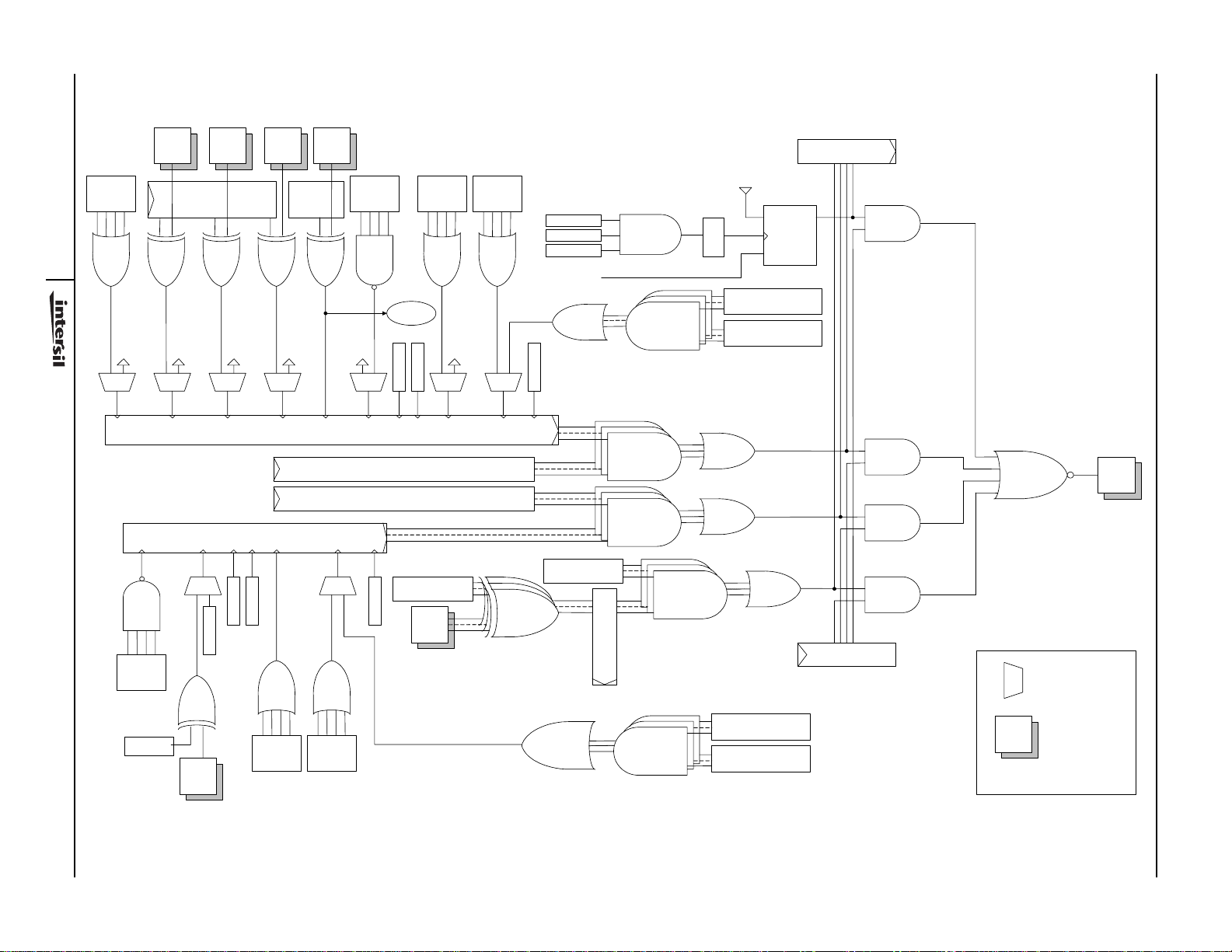
FIGURE 5. LASI EQUIVALENT SCHEMATIC
www.BDTIC.com/Intersil
(See Also Figure 4)
18
REG.
4.C00Ah.
3:0
PHY XS
LOS
(SIG DET)
CX4
OPTX
LBC
ALARM PIN POLARITY
LX4
LX4
Clear on read
Clear on read
REGISTER 1.9003h.[6:0] RX_ALARM_STATUS
PCS
BYTE
SYNCH
REG
3.24
[3:0]
REG
1.C01Dh.3
OPT
TEMP
REG 1.C01Dh.2:0
CX4
LX4
CX4
LX4
REG 1.10.0
OPRX
OP
CX4
REG 1.8.10
OPTX
LOP
LX4
REGISTER 1.9004h.[10:0] TX_ALARM_STATUS
REG 3.8.10
PCS
CODE
ERROR
REG.
3.C007h.
7:4
TX_
FAULT
Latch on high
CX4
LX4
PCS
FIFO
REG.
11:8
REG.
4.24.3:0
PHY XS
BYTE
SYNCH
CX4
LX4
REG 4.8.10
See IEEE
REG 1.8.11
REG 1.C012h.[12:8]
GPIO POLARITY
REG
1.C012h.13
POLARITY
CX4
REGISTER 1.9001h[10:0] TX_ALARM CONTROL
REGISTER 1.9000h[6:0] RX_ALARM CONTROL
ERROR
3.C007h.
REG.
4.C007h.
PHY XS
FIFO
ERROR
REG 3.8.11
GPIO
[4:0]
11:8
CX4
LX4
Latch on high
REG.
4.C007h.
7:4
PHY XS
CODE
ERROR
CX4
LX4
REG 4.8.11
RX_FLAG
REG. 3.24.12
REG. 1.10.0
REG. 4.24.12
TX_FLAG
REG 1.C012h.[4:0]
GPIO-LASI EN
Latch
hi
GPIO INPUT
LINK
STATUS
Clear on Read of 1.9005
REG 1.C011h.[12:8]
Change
Clock on
any
change
REG 1.9006h[7:0]
TX_FLAG CONTROL
REG 1.A070h[7:0]
TX_FLAG
TX_ALARM
RX_ALARM
GPIO->LASI
REG 1.9007h[7:6]
RX_FLAG CONTROL
REG 1.A074h[7:6]
RX_FLAG
D
LS_ALARM
CLK
CLR
REG 1.9005h[3:0]
LASI STATUS
Q
REG 1.9002h[3:0]
LASI CONTROL
LS ALARM
Masked
TX ALARM
Masked
RX ALARM
Masked
GPIO
ALARM
Masked
LX4
CX4
LASI
Legend
Selector for
CX4 vs LX4
External Pad
BBT3821
LASI
BBT3821
www.BDTIC.com/Intersil
Writing EEPROM Space through the I2C Interface
The BBT3821 permits two methods for writing the requisite
values into EEPROM or other I
space into the I
2
C register space. Many DOM circuits protect
their important internal data through some form of password
protection, and in general the BBT3821 will allow this to be
done without a problem.
BLOCK WRITES TO EEPROM SPACE
The first method is applicable only to the NVR space (I
address space A0.00:FF’h). If the WRTP (Write Protect) pin is
inactive (low), and the NVR Write Size bit (1.32773.7 =
1.8005.7’h) is set to a ‘1’, then issuing a ‘Write All NVR’
command (write 0023’h to 1.32768 = 1.8000’h) will write the
current contents of MDIO registers 1.8007:8106’h into the NVR
space. The ‘NVR Write Page Size’ bits in 1.32773.1:0
(1.8005.1:0’h) control the block size used for the write
operation. See Figure 21 for the sequence timing. Normally this
operation is only useful for initialization of a module EEPROM
space, but it could be used for field upgrades or the like. If the
WRTP (Write Protect) pin is high (active, normal condition), OR
the Write Size bit (1.32773.7 = 1.8005.7’h) is cleared to a ‘0’,
then issuing a ‘Write All NVR’ command (write 0023’h to
1.32768 = 1.8000’h) will write only the current contents of the
MDIO register block within 1.807F:80AE’h to the XENPAKdefined Customer Area, A0.77:A6’h. The actual block write will
occur one byte at a time. The block write size controls cannot
be used here, since the Customer Area block boundaries do
not lie on page-write boundaries of the EEPROM, a feature of
the XENPAK specification.
BYTE WRITES TO EEPROM SPACE
The second method is applicable to any part of the I
The write operation is performed one byte at a time. The device
address and memory address are written into the 1.32769
2
C devices from the MDIO
2
C space.
2
C
(1.8001’h) and 1.32770 (1.8002’h) registers respectively (see
Table 16 and Table 17), and the data to be written into the
1.32772 (1.8004’h) register. On issuing a ‘Write one byte’
command (write 0022’h to 1.32768 = 1.8000’h) the data will be
written into the I
2
C space. See Figure 23 for the timing
sequence. Note that if the WRTP (Write Protect) pin is high, or
the Write Size bit (1.32773.7 = 1.8005.7’h) is cleared to a ‘0’,
writes to any part of the basic NVR space outside the XENPAKdefined Customer Area will be ignored. Also note that a 16-bit
addressable EEPROM (or equivalent) device on the I
2
C bus
may be written by setting the Long Memory bit 1.32773.8
(1.8005.8’h) to a ‘1’, and writing a full 16-bit memory address
value into 1.32770 (1.8002’h). Note that this 16-bit operation
MUST NOT be used on an 8-bit device.
These one-byte operations could be used to load modified
Device Address values or protective passwords into multiple
DOM devices, or for loading other types of data into them. They
are also useful for writing data into I
2
C interface DCP devices
for setting laser currents, etc.
MDIO Registers
In the following tables, the addresses are given in the table
headers both in decimal (as used in the IEEE 802.3ae and
802.3ak documents) and in hexadecimal form. Where the
registers coincide in structure and meaning, but the Device
Addresses differ, the underlying register bits are the same, and
may be read or written indiscriminately via any relevant Device
Address. For instance a full RESET may be initiated by writing
any one of 1.0.15, 3.0.15, or 4.0.15. While the reset is active,
reading any of these bits would return a ‘1’ (except that the
reset lasts less than the MDIO preamble plus frame time).
When the reset operation is complete, reading any of them will
return a ‘0’. Note that extra preambles may be required after
such a software RESET (see Figure 17).
Table 4. MDIO PMA/PMD DEVAD 1 REGISTERS
PMA/PMD DEVICE 1 MDIO REGISTERS
ADDRESS
NAME DESCRIPTION DEFAULT AC
1.0 1.0 PMA/PMD Control 1 Reset, Enable serial loop back mode. 2040’h R/W Table 5
1.1 1.1 PMA/PMD Status 1 Local Fault and Link Status 0004’h
1.2:3 1.2:3 ID Code Manufacturer OUI & Device ID 01839C6V’h RO See
1.4 1.4 Speed Ablty PMA/PMD Speed Ability 0001’h RO Table 7
1.5 1.5 Dev in Pkg. Devices in Package, Clause 22. 001A’h RO Table 8
1.6 1.6 Vend Sp Dev Vendor Specific Devices in Package 0000’h RO Table 8
1.7 1.7 PMA/PMD Control 2 PMA/PMD type Selection P
1.8 1.8 PMA/PMD Status 2 Fault Summary, Device Ability B311’h
1.9 1.9 PMD TX Dis Disable PMD Transmit 0000’h R/W Table 11
1.10 1.A PMD Sig Det PMD Signal Detect 001F’h
19
(4)
(2)
(2)
(2)
(5)
R/W DETAILSDEC HEX
RO/LL Table 6
(6)
RO
RO
(LH)
RO Table 12
(1)
Ta bl e 9
Ta bl e 1 0

BBT3821
www.BDTIC.com/Intersil
Table 4. MDIO PMA/PMD DEVAD 1 REGISTERS (Continued)
PMA/PMD DEVICE 1 MDIO REGISTERS
ADDRESS
NAME DESCRIPTION DEFAULT AC
1.11 1.B PMD Ext Ca PMD Extended Capability 0001’h RO Table 13
1.14:15 1E:F Pkg OUI PMD Package OUI, etc. 00000000’h
1.32768 1.8000 NVR Cntrl NVR Control & Status Register 0003’h R/W Table 15
2
1.32769 1.8001 I
1.32770 1.8002 I
1.32771 1.8003 I
1.32772 1.8004 I
1.32773 1.8005 I
1.32774 1.8006 I
1.32775:
33030
1.36864 1.9000 RX Al Ctrl RX ALARM Control See Table
1.36865 1.9001 TX Al Ctrl TX ALARM Control See Table
1.36866 1.9002 LASI Ctrl LASI Control 0000’h A R/W Table 26
1.36867 1.9003 RX Al Stts RX ALARM Status 0000’h
1.36868 1.9004 TX Al Stts TX ALARM Status 0000’h
1.36869 1.9005 LASI Stts LASI Status 0000’h
1.36870 1.9006 DOM TX DOM TX_Flag Control 0000’h A R/W Table 30
1.36871 1.9007 DOM RX DOM RX_Flag Control 0000’h A R/W Table 31
1.40960:
41215
1.41216 1.A100 DOM Ctrl DOM Control & Status 0000’h R/W Table 38
1.49153 1.C001 PMA Ctrl2 PMA Control 2 0000’h A R/W Table 39
1.49156 1.C004 PMA LB PMA Loopback Control 0000’h A R/W Table 40
1.49157 1.C005 PMA Pre PMA Pre-emphasis Control See Table
1.49158 1.C006 PMA Eql PMA Equalizer Boost Control See Table
1.49162 1.C00A SIG_DET Signal Detect Flags 0000’h
1.49163 1.C00B Fine Tune Adjust pre-emphasis, amplitude See Table
1.49167 1.C00F Soft RST Soft RESET 0000’h R/W Table 46
1.49168:
49171
1.49176 1.C018 DOM Control DOM Control Register 0000’h A R/W Table 51
1.49177:8 1.C019:A DOM Mem DOM Indirect Start Addresses 6060’h A R/W Table 53
1.49179:80 1.C01B:C DOM Dev DOM Indirect Device Addresses See Tables A R/W Table 54
1.49181 1.C01D StatusPolrty LASI Alarm Pin Polarity 0000’h A R/W Table 55
Note (1): V’ is a version number. See “JTAG & AC-JTAG Operations” on page 53 for a note about the version number.
Note (2): Read values depend on status signal values. Values shown indicate ‘normal’ operation.
Note (3): If NVR load operation succeeds, will be overwritten by value loaded, see Table 22.
Note (4): Default value depends on CX4/LX4 select LX4_MODE Pin Value.
Note (5): For rows with “A”, the default value may be overwritten by the Auto-Configure opera tion (See “Auto-Configuring Control Registers” on page 16 and Tabl e92
Note (6): IEEE 802.3 shows as R/W, but ca nnot write any other value than that set by LX4_MODE Pin.
1.8007:
8106
1.A000
:A0FF
1.C010
:C013
for details).
C Dev Ad 1-Byte Operation Device Addr. A2’h R/W Table 16
2
C Mem Ad 1-Byte Operation Memory Addr. 0000’h R/W Table 17
2
C RD Data 1-Byte Operation Read Data 0000’h RO Table 18
2
C WR Data 1-Byte Operation Write Data 0000’h R/W Table 19
2
C Op Ctl I2C Operation Control 004D’h R/W Table 20
2
C Op Stts I2C Operation Status 0000’h RO/LH Table 21
NVR Copy
Registers
DOM Copy
Registers
GPIO Cnfg GPIO Config, Status & Alarm Registers 0000’h
XENPAK NVR Register Copies Set by
EEPROM
Alarm & Warning Thresholds, A/D
Values, (cf SFF-8472)
Set by DOM
devices
(3)
(4)
(4)
(2)
(2)
(2)
(4)
(4)
(2)
(4)
(2)
(5)
R/W DETAILSDEC HEX
R/W Table 14
R/W Table 22
AR/WTable24
AR/WTable25
RO Table 27
RO Table 28
RO Table 29
RO Table 32:
Ta bl e 3 7
AR/WTable41
AR/WTable43
RO Table 44
AR/WTable45
A R/W Table 47:
Ta bl e 5 0
20

BBT3821
www.BDTIC.com/Intersil
IEEE PMA/PMD REGISTERS (1.0 TO 1.15/1.000F’H)
Table 5. IEEE PMA/PMD CONTROL 1 REGISTER
MDIO REGISTER ADDRESS = 1.0 (1.0000’h)
BIT(S) NAME SETTING DEFAULT R/W DESCRIPTION
1.0.15
3.0.15
4.0.15
1.0.14 Reserved 0’b
1.0.13 Speed Select 1 = 10Gbps 1’b RO 1 = bits 5:2 select speed
1.0.12 Reserved 0’b
1.0.11 LOPOWER 0 = Normal Power 0’b R/W No Low Power Mode, writes ignored
1.0.10:7 Reserved 0’h
1.0.6 Speed Select 1 = 10Gbps 1’b RO 1 = bits 5:2 select speed
1.0.5:2 Speed Select 0000 = 10Gbps 0’h RO Operates at 10Gbps
1.0.1 Reserved 0’b
1.0.0 PMA Loopback 1 = Enable loopback
Note (1): After this RESET bit is written, the BBT3821 will not begin counting PREAMBLE bits immediately. See Figure 17 for details.
Reset 1 = reset
0 = reset done, normal
operation
0 = Normal operation
0’b R/W SC Writing 1 to this bit will reset the whole chip,
including the MDIO registers.
0’b R/W Enable serial loop back mode on all four lanes,
XAUI in to XAUI out.
(1)
Table 6. IEEE PMA/PMD STATUS 1 REGISTER
MDIO REGISTER ADDRESS = 1.1 (1.0001’h)
BIT NAME SETTING DEFAULT R/W DESCRIPTION
1.1.15:8 Reserved 00’h
1.1.7 Local Fault 1 = PMA Local Fault 0’b RO Derived from Register 1.8.11:10
1.1.6:3 Reserved 0’h
1.1.2 Rx Link Up 1 = PMA Rx Link Up
1.1.1 LoPwrAble Low Power Ability 0’b RO Device does not support a low power mode
1.1.0 Reserved 0’b
Note (1): This bit is latched low on a detected Fault condition. It is set high on being read.
BIT NAME SETTING DEFAULT R/W DESCRIPTION
1.4.15:3
3.4.15:2
4.4.15:1
1.4.2:1
3.4.1
1.4.0
3.4.0
4.4.0
Reserved for future
speeds
10PASS-T2/
2BASE-TL
10GbpsAble 10Gbps Ablility 1’b RO Device Able to operate @ 10Gbps
0 = PMA/D Rx Link Down
Table 7. IEEE PMA/PMD, PCS, PHY XS, SPEED ABILITY REGISTER
MDIO REGISTER ADDRESSES = 1.4, 3.4 & 4.4 ([1,3,4].0004’h)
EFM Ability 00’b RO Device cannot operate @ 2BASE-TL or 10PASS-
1’b
000’h
(1)
RO LL
(1)
‘Up’ means CX4/LX4 signal level is OK, and the
PLL locked
T2
21

BBT3821
www.BDTIC.com/Intersil
Table 8. IEEE DEVICES IN PACKAGE REGISTERS
MDIO REGISTER ADDRESSES = 1.5, 3.5, 4.5 ([1,3:4].0005’h)
BIT NAME SETTING DEFAULT R/W DESCRIPTION
[1,3:4].5.15:8 Reserved 000’h
[1,3,4].5.7 Link Partner Link Partner PMA/PMD present 0’b RO Device has no Link Partner
[1,3,4].5.6 10PASS-TS tone table 10PASS-TS tone table present 0’b RO Device has no 10PASS-TS tone table
[1,3:4].5.5 DTE XS DTE XS Present 0’b RO Device ignores DEVAD 5
[1,3:4].5.4 PHY XS PHY XS Present 1’b RO Device responds to DEVAD 4
[1,3:4].5.3 PCS PCS Present 1’b RO Device responds to DEVAD 3
[1,3:4].5.2 WIS WIS Present 0’b RO Device ignores DEVAD 2
[1,3:4].5.1 PMD_PMA PMD/PMA Present 1’b RO Device responds to DEVAD 1
[1,3:4].5.0 Cls_22 Clause 22 registers 0’b RO Device ignores Clause 22
MDIO REGISTER ADDRESSES = 1.6, 3.6, 4.6 ([1,3:4].0006’h)
[1,3:4].6.15 VndrDEV2 Vendor Specific DEV2 0’b RO Device ignores DEVAD 31
[1,3:4].6.14 VndrDEV1 Vendor Specific DEV1 0’b RO Device ignores DEVAD 30
[1,3,4].6.13 Clause 22 extn. Clause 22 extension 0’b RO Device has no Clause 22 extension
[1,3:4].6.12:0 Reserved 000’h
Table 9. IEEE PMA/PMD TYPE SELECT REGISTER
MDIO REGISTER ADDRESSES = 1.7 (1.0007’h)
BIT NAME SETTING DEFAULT R/W DESCRIPTION
1.7.15:4 Reserved 000’h
(1)
1.7.3:0 PMA/PMD Type 0100 = 10GBASE-LX4
0000 = 10GBASE-CX4
Note (1): Value depends on the current state of the LX4/CX4 select LX4_MODE pin. Although IEEE 802.3ae specifies R/W bits, only valid values may be written; since
the pin controls the available valid value, no meaningful write is possible.
Table 10. IEEE PMA/PMD STATUS 2 DEVICE PRESENT & FAULT SUMMARY REGISTER
MDIO REGISTER ADDRESSES = 1.8 (1.0008’h)
BIT NAME SETTING DEFAULT R/W DESCRIPTION
1.8.15:14 Device present 10 = Device present 10’b RO When read as “10”, it indicates that a device is
1.8.13 TXLocalFlt Ability 1 = PMA/PMD can detect TX
Fault
1.8.12 RXLocalFlt Ability 1 = PMA/PMD can detect RX
Fault
1.8.11 TXLocalFlt 1 = TX Local Fault; on Egress
channel
1.8.10 RXLocalFlt 1 = RX Local Fault; on Ingress
channel
1.8.9 Ext Ability 1 = Extended Ability Register
present.
1.8.8 TX Disable 1 = Can Disable TX 1’b RO Device can Disable Transmitter
1.8.7 10GBASE-SR 0 = cannot perform 0’b RO Device cannot be 10GBASE-SR
1.8.6 10GBASE-LR 0 = cannot perform 0’b RO Device cannot be 10GBASE-LR
1’b RO PMA/PMD has the ability to detect a Local Fault
1’b RO PMA/PMD has the ability to detect a Local Fault
0’b RO LH
0’b RO
1’b RO Device has Extended Ability Register in 1.11
RO LX4_MODE select pin high is LX4 value,
P’b
low is CX4 value
present at this device address
on Transmit Path
on Receive Path
(1)
PLL lock fail (missing REFCLK) or TX_FAULT pin
active
PLL lock fail (missing REFCLK), or Loss of Signal
in 1.10 (1.000A’h)
(1.000B’h)
LH
(1,2)
22
BBT3821
www.BDTIC.com/Intersil
Table 10. IEEE PMA/PMD STATUS 2 DEVICE PRESENT & FAULT SUMMARY REGISTER (Continued)
MDIO REGISTER ADDRESSES = 1.8 (1.0008’h)
BIT NAME SETTING DEFAULT R/W DESCRIPTION
1.8.5 10GBASE-ER 0 = cannot perform 0’b RO Device cannot be 10GBASE-ER
1.8.4 10GBASE-LX4 1 = can perform 1’b RO Device can be 10GBASE-LX4
1.8.3 10GBASE-SW 0 = cannot perform 0’b RO Device cannot be 10GBASE-SW
1.8.2 10GBASE-LW 0 = cannot perform 0’b RO Device cannot be 10GBASE-LW
1.8.1 10GBASE-EW 0 = cannot perform 0’b RO Device cannot be 10GBASE-EW
1.8.0 PMA Loopback 1 = can perform 1’b RO Device can perform PMA loopback
Note (1): These bits are latched high on any Fault condition detected. They are reset low (cleared) on being read. They will also be reset low on reading the LASI
Note (2): The source of ‘Loss of Signal’ depends on the LX4/CX4 select LX4_MODE pin (see register 1.10, 12, note (1) below).
Note (1): In CX4 mode the TCXnP/N pin outputs will be disabled; in LX4 Mode only TX_ENA[n] pin is disabled.
registers 1.9003’h (bit 10, see Table 27) or 1.9004’h (bit 11, see Table 28).
Table 11. IEEE TRANSMIT DISABLE REGISTER
MDIO REGISTER ADDRESS = 1.9 (1.0009’h)
BIT NAME SETTING DEFAULT R/W DESCRIPTION
1.9.15:5 Reserved
1.9.4 PMD Dis 3 Disable TX on Lane 3
1.9.3 PMD Dis 2 Disable TX on Lane 2
1.9.2 PMD Dis 1 Disable TX on Lane 1
1.9.1 PMD Dis 0 Disable TX on Lane 0
1.9.0 PMD Dis All Disable TX on all 4 Lanes 0’b R/W
(1)
(1)
(1)
(1)
0’b R/W 1 = Disable PMD Transmit on respective Lane
0’b R/W
0’b R/W
0’b R/W
0 = Enable PMD Transmit on respective Lane
(unless TXON/OFF pin is Low)
(1)
Table 12. IEEE PMD SIGNAL DETECT REGISTER
MDIO REGISTER ADDRESS = 1.10 (1.000A’h)
BIT NAME SETTING DEFAULT R/W DESCRIPTION
1.10.15:5 Reserved
1.10.4 PMD Rx Ln 3 PMD Signal Det’d 1’b
1.10.3 PMD Rx Ln 2 PMD Signal Det’d 1’b
1.10.2 PMD Rx Ln 1 PMD Signal Det’d 1’b
1.10.1 PMD Rx Ln 0 PMD Signal Det’d 1’b
1.10.0 PMD Rx Glob PMD Signal Det’d 1’b
Note (1): These bits reflect the OPRLOS[3:0] pins (Table 99) in LX4 mo de, or the CX4 SIGNAL_DETECT function in CX4 mode, dependi ng on the LX4_MODE select pin.
Table 13. IEEE EXTENDED PMA/PMD CAPABILITY REGISTER
MDIO Register Addresses = 1.11 (1.000B’h)
BIT NAME SETTING DEFAULT R/W DESCRIPTION
1.11.15:1 Reserved 0000’h RO
(1)
1.11.0
Note (1): These values reflect the IEEE 802.3ak 10GBASE-CX4 specification.
10GBASE-CX4 1 = can perform 1’b RO Device can be 10GBASE-CX4
(1)
(1)
(1)
(1)
(1)
RO 1 = PMD Signal Detected on respective Lane
RO
RO
RO
RO
(Global, all Lanes)
0 = PMD Signal not detected on respective Lane
(Global, any
Lane)
(1)
23

BBT3821
www.BDTIC.com/Intersil
Table 14. IEEE PACKAGE IDENTIFIER REGISTERS
MDIO REGISTER ADDRESSES = 1.14:15 (1.000E:F’h)
BIT NAME SETTING DEFAULT R/W DESCRIPTION
1.14.15:0 Package ID Package OUI bits 3:24 &
1.15.15:0 Package ID 00’h R/W
etc.
XENPAK-DEFINED REGISTERS (1.8000’H TO 1.8106’H)
Table 15. XENPAK NVR CONTROL & STATUS REGISTER
MDIO (XENPAK) REGISTER ADDRESS = 1.32768 (1.8000’h)
BIT NAME SETTING DEFAULT R/W DESCRIPTION
1.32768.15:6 Reserved 000’h R/W
(1)
1.32768.5 NVR Command
1.32768.4 Reserved 0’b RO
1.32768.3:2 NVR Command
1.32768.1:0 Extended NVR
Note (1): User writes to these bits are not valid unless the Command Status is Idle. The Command Status will not return to Idle until read after command completion
(either Succeed or Failed).
Note (2): At the end of a hardware RESET via the RSTN pin, on powerup, or on a register [1,3,4].0.15 RESET operation, and if the XP_ENA pin is asserted, the
BBT3821 will automatically begin an ‘all NVR read’ operation.
Note (3): The single byte commands are controlled through the bits of the registers at 1.32769: 32774 (1.800 1:8006 ’h). The ‘b lock write/read’ commands are affected by
register 1.32773 (1.8005’h). Additional status is available in 1.327743 (1.8006’h)
(3)
Status
Command
1 = Write NVR
0 = Read NVR
Current Status of
NVR Command
NVR operation to be
performed
00’h R/W If NVR is loaded, these are copies of
1.32818:32819 (1.8032:8033’h) & 1.32820:32821
(1.8034:8035’h)
(2)
0’b
00’b RO 11 = Command failed
(2)
11’ b
R/W Write/Read Control for I2C operation
10 = Command in progress/Queued
01 = Command completed with success
00 = Idle
R/W 10 = read/write one byte
11 = read/write all NVR contents
Other values = reserved
(3)
(3)
Table 16. I2C ONE-BYTE OPERATION DEVICE ADDRESS REGISTER
MDIO REGISTER ADDRESS = 1.32769 (1.8001’h)
BIT NAME SETTING DEFAULT R/W DESCRIPTION
1.32769.15:8 Reserved 00’h RO
2
1.32769.7:0 Device
BIT NAME SETTING DEFAULT R/W DESCRIPTION
1.32770.15:0 Memory
Note (1): 8-bit-addressed I
BIT NAME SETTING DEFAULT R/W DESCRIPTION
1.32771.15:8 Reserved 00’h RO
1.32771.7:0 Read Data I
Address
Address
2
C devices are addressed using bits 7:0. Never set bit 1.32773.8 (1.8005’h.8) for 16-bit address operation with an 8-bit address I2C device.
C Device address to
I
access
Table 17. I2C ONE-BYTE OPERATION MEMORY ADDRESS REGISTER
MDIO REGISTER, ADDRESS = 1.32770 (1.8002’h)
2
C Memory address to
I
access
Table 18. I2C ONE-BYTE OPERATION READ DATA REGISTER
MDIO REGISTER ADDRESS = 1.32771 (1.8003’h)
2
C Read Data 00’h RO Result of I2C 1-byte Read operation
A2’h R/W All I2C Device addresses are even. Bit 0 cannot be set.
(2)
0000’h
R/W I2C Memory Address within Device address of 1.32769
(1.8001’h)
24

BBT3821
www.BDTIC.com/Intersil
Table 19. I2C ONE-BYTE OPERATION WRITE DATA REGISTER
MDIO Register Address = 1.32772 (1.8004’h)
BIT NAME SETTING DEFAULT R/W DESCRIPTION
1.32772.15:8 Reserved 00’h RO
2
1.32772.7:0 Write Data I
BIT NAME SETTING DEFAULT R/W DESCRIPTION
1.32773.15:9 Reserved 00’h RO
1.32773.8 Long Memory
1.32773.7 NVR Write Size 0’b R/W 1 = Block write all 256 bytes to NVR
1.32773.6:4 I2C Bus Speed Speed of I2C SCL
1.32773.3:2 NVR ACK Error
Count
1.32773.1:0 NVR Write Page
Size
(2)
C Write Data 00’h R/W Data to be written by 1-byte Write Operation
Table 20. NVR I2C OPERATION CONTROL REGISTER
MDIO REGISTER ADDRESS = 1.32773 (1.8005’h)
(1)
1 =16 bit
0 = 8 bit
(4)
(derived
clock
from REF_CLOCK)
11 = 63
10 = 16
01 = 4
00 = 1
11 = 32 bytes
10 = 16 bytes
01 = 8 bytes
00 = 4 byte
0’b R/W Length of address for I2C device selected
0 = Write only 1.807F:AE’h to NVR
100’b R/W 111 = 400kHz
110 = 200kHz
101 = 150kHz
100 = 100kHz
11’b R/W Number of ACK failures at any address before I
01’b R/W The I
Operation failure is reported
2
C interface block write operation will issue a
STOP and wait for the EEPROM every time after this
number of bytes are sent out
011 = 40kHz
010 = 20kHz
001 = 10kHz
000 = 4kHz
(3)
(2)
2
C
Note (1): This bit should only be set if an I2C device which needs a 16-bit address is to be addressed. The NVR and DOM spaces are all 8-bit address sections , and for
Note (2): Block 256-byte NVR writes will not occur unless the WRTP pin is set Low. NVR Write Page Size controls Page size for Block operations only.
Note (3): This area corresponds to the XENPAK-defined Customer Area; see XENPAK Spec R3.0 Section 10.12.22. Writes will be performed one byte at a time.
Note (4): The I
Note (1): These bits are latched high on any internal error condition detected. They are reset low (cleared) on being read.
Note (2): These bits are set if the EXOR sum calculated from the indicated range is not the same as the value read into the listed checksum register. Note that this is
these areas, this bit should be 0’b.
2
C clock speeds listed are approximate. They are derived by division from the CMU, locked to the RFCP/N inputs. At 156.25MHz, the nominal 100kHz
clock will actually be 156.25/1.6kHz, just over 97. 5kHz. See also the notes to Table 117.
Table 21. NVR I2C OPERATION STATUS REGISTER
MDIO REGISTER ADDRESS = 1.32774 (1.8006’h)
BIT NAME SETTING DEFAULT R/W DESCRIPTION
1.32774.15 XP_ENA XP_ENA pin RO 1 = XP_ENA pin high, 0 = low
1.32774.14:4 Reserved 0000’h RO
1.32774.3 Vendor Specific
Area EXOR sum check
1.32774.2 Customer Write Area
EXOR sum check
1.32774.1 Reserved 0’b RO
1.32774.0 NVR Area EXOR sum
check
NOT the same as the XENPAK-defined checksum calculation. Contact Intersil for a method of reconciling these two checksum calculations.
Error Flag 0’b RO LH 1 = 1.8106 ! =
0 = 1.8106 =
Error Flag 0’b RO LH 1 = 1.80AD ! = EXOR(1.807E:80AC)
LH
Error Flag 0’b RO LH 1 = 1.807D ! = EXOR(1.8007:807C)
0 = 1.80AD =
(1)
0 = 1.807D =
EXOR(1.80AE:8105)
EXOR(1.80AE:8105)
EXOR(1.807E:80AC)
EXOR(1.8007:807C)
(2)
(2)
(2)
25

BBT3821
www.BDTIC.com/Intersil
Table 22. XENPAK NVR REGISTER COPY
MDIO XENPAK/XPAK/X2 NVR REGISTER ADDRESSES = 1.32775:33030 (1.8007:8106’h)
BYTE ADDRESS
NAME DESCRIPTION
1.32775 to
1.32817
1.32818 to
1.32821
1.32822 to
1.32889
1.32890 1.807A DOM Ctrl DOM Capability Bits R/W
1.32891
1.32892
1.32893 1.807D Basic Chksm Basic Field Checksum
1.32894 to
1.32940
1.32941 1.80AD Cstm Chksm Customer Area Checksum
1.32942 to
1.33027
1.33028 1.8104 A/C Size Auto-configure Size (N) See page 16
1.33029 1.8105 A/C Pointer Auto-configure Pointer (S)
1.33030 1.8106 Vndr Chksm Vendor Specific Checksum
1.8007 to
1.8031
1.8032 to
1.8035
1.8036 to
1.8079
1.807B
1.807C
1.807E to
1.80AC
1.80AE to
1.8103
NVR Register
Copy
PKG OUI XENPAK/XPAK/X2 Package OUI (bits 3 to
NVR Register
Copy
NVR Reg Copy XENPAK NVR Register Copies R/W
NVR Register
Copy
NVR Register
Copy
XENPAK NVR Register Copies R/W
24)
XENPAK NVR Register Copies R/W
Customer Writable Area
Vendor Specific Area R/W
(1)
(3)
Σ(1.8007:807C)
(4)
(5)
(6)
Σ(1.80AE:8105)
SUGGESTED VALUE R/W DETAILSDEC HEX
Xenpak = 0008BE
XPAK = 000ACB
X2 = 000C64
Σ(1.807E:80AC)
(or 00 or FF’h)
R/W
R/W
(2)
(2)
Mirrored to 1.14:15
(1.E:F’h)
(2)
(2)
Table 23
(2)
(2)
(2)
See Table 92
Note (1): Only register values operated on by the BBT3821 are individually listed. The others are merely copied from the I2C NVR space.
Note (2): Although data can be written to these registers, it will be volatile, unless the ‘Write NVR’ operation as specified in
Note (3): Checksum to be calculated from 1.8007’h to 1.807C’h. Host can check for validity.
Note (4): If WRTP pin is high, this is the only area that can be written by the user. See also Note (2) above.
Note (5): Checksum to be calculated from 1.807E’h to 1.80AC’h.
Note (6): Checksum to be calculated from 1.80AE’h to 1.8105’h.
Note (1): Suggested values are given, for a full LX4 module with four individual-lane DOM circuits, at least one having the DOM data at Device Address A2’h.
Note (2): Last three significant bits of the (default) DOM I
Note (3): Although data can be written to this register, it should only be done for writing the NVR, using the ‘Write NVR’ operation as specified in “Writing EEPROM Space
Interface” on page 19
BIT NAME SETTING
1.32890.15:8 Reserved 000’h
1.32890.7 DOM Ctrl Reg 1 = Implemented
1.32890.6 DOM system 1’b R/W DOM Implemented
1.32890.5 Lane-by Lane 1’b R/W WDM Lane-by-Lane DOM; registers 1.A0C0:A0FF’h
1.32890.4 LBC Scale 1 = 10µA
1.32890.3 Reserved
1.32890.2:0 DOM Address 001’b R/W I
(A0’h + 2*(<1.32890.2:0>). A device MUST be present at this address for correct operation if bit 6 is set.
through the I2C Interface” on page 19. The values here should normally only be loaded from the NVR, since they could affect the operation of the BBT3821 if
incorrect.
is performed.
Table 23. XENPAK DIGITAL OPTICAL MONITORING (DOM) CAPABILITY REGISTER
MDIO (XENPAK) REGISTER, ADDRESS = 1. 32890 (1. 807A’h)
SUGGESTED
1’b R/W DOM Control/Status Register 1.A100’h
0 = Not
implemented
0 = 2µA
2
C Device Address (NB LSB is a read/write flag). Upper bit s are assumed to be ‘1010’b, Device address will be
VAL UE
(1)
R/W
(3)
valid
R/W Laser Bias Scale Factor
2
C Device Address of (initial) DOM IC
“Writing EEPROM Space through the I2C
DESCRIPTION
(2)
26

BBT3821
www.BDTIC.com/Intersil
XENPAK LASI AND DOM REGISTERS (1.9000’H TO 1.9007’H & 1.A000’H TO 1.A100’H)
Table 24. XENPAK LASI RX_ALARM CONTROL REGISTER
MDIO REGISTER, ADDRESS = 1.36864 (1.9000’h)
(1)
BIT NAME SETTING DEFAULT
1.36864.15:7 Reserved 000’h
1.36864.6 PCS Byte S 1 = trigger LASI by
1.36864.5 RX Power 1’b R/W Receive Laser Pwr/Sig Det LASI Enable
1.36864.4 PMA LF 1’b R/W PMA RX Local Fault LASI Enable
1.36864.3 PCS LF 1’b R/W PCS RX Local Fault LASI Enable
1.36864.2 PCS Code 0’b/1’b R/W 8b/10b Code Violation LASI Enable
1.36864.1 DOM RX 1’b R/W DOM RX or RX EFIFO Fault LASI Enable
1.36864.0 PHY RX LF 1’b R/W PHY RX Local Fault LASI Enable
corresponding bit of
1.36867 (1.9003’h)
0 = LASI ignores
corresponding bit of
1.36867 (1.9003’h)
0’b R/W PCS Byte Sync Fail LASI Enable
R/W DESCRIPTION
Note (1): Where two values are given, Default depends on LX4/CX4 select LX4_MODE pin. First value is LX4 value. The value may be overwritten by the Auto-
Note (1): Where two values are given, Default depends on LX4/CX4 select LX4_MODE pin. First value is LX4 value. The value may be overwritten by the Auto-
Configure operation (See “Auto-Configuring Control Registers” on page 16 and Table92 for details).
Table 25. XENPAK LASI TX_ALARM CONTROL REGISTER
MDIO REGISTER, ADDRESS = 1.36865 (1.9001’h)
(1)
BIT NAME SETTING DEFAULT
1.36865.15:11 Reserved 000’h
1.36865.10 PHY S_D 1 = trigger LASI from
1.36865.9 LBC 1’b/0’b R/W Laser Bias Current Fault LASI Enable
1.36865.8 LTEMP 1’b/0’b R/W Laser Temperature Fault LASI Enable
1.36865.7 LOP 1’b/0’b R/W Laser Output Power Fault LASI Enable
1.36865.6 TX LF 1’b/0’b R/W Transmit Local Fault LASI Enable
1.36865.5 Byte Sync 0’b/1’b R/W PHY XS Byte Sync Fail LASI Enable
1.36865.4 PMA LF 1’b R/W PMA TX Local Fault LASI Enable
1.36865.3 PCS LF 1’b/0’b R/W PCS TX Local Fault LASI Enable
1.36865.2 TX EFIFO 0’b/1’b R/W Transmit EFIFO Error LASI Enable
1.36865.1 DOM TX/
PHY Code
1.36865.0 PHY TX LF 1’b R/W PHY TX Local Fault LASI Enable
Configure operation (See “Auto-Configuring Control Registers” on page 16 and Table92 for details).
corresponding bit of
1.36868 (1.9004’h)
0 = LASI ignores
corresponding bit of
1.36868 (1.9004’h)
0’b/1’b R/W PHY XS Signal Detect LASI Enable
1’b R/W DOM TX or PHY XS 8b/10b Code Violation Fault LASI
R/W DESCRIPTION
Enable
Table 26. XENPAK LASI CONTROL REGISTER
MDIO REGISTER, ADDRESS = 1.36866 (1.9002’h)
(1)
BIT NAME SETTING DEFAULT
1.36866.15:4 Reserved 000’h
1.36866.3 GPIO 1 = trigger LASI via bit in
1.36866.2 RX_Alarm 0’b R/W Enable RX_Alarm to trigger LASI
1.36866.1 TX_Alarm 0’b R/W Enable TX_Alarm to trigger LASI
1.36866.0 LS_Alarm 0’b R/W Enable Link Status change to trigger LASI
Note (1): The default values may be ov erwritten by the Auto-Configure operation (See “A uto-Configuring Control Registers” on page 16 and Table 92 for details). Since
on Power up or RESET several LASI contributors will initially be in the ‘fault’ condition (in particular, Byte Synch and Lane Alignment, and their derivatives), it
may be advisable for a host to clear these before enabling these to trigger LASI.
Note (2): See description of the General Purpose Input/Output (GPIO) pins and bits for a description of how they contribute to the LASI system.
1.36869 (1.9005’h)
0 = LASI ignores bit
0’b R/W Enable GPIO pins to trigger LASI
R/W DESCRIPTION
27
(2)

BBT3821
www.BDTIC.com/Intersil
Table 27. XENPAK LASI RX_ALARM STATUS REGISTER
MDIO REGISTER, ADDRESS = 1.36867 (1.9003’h)
(3)
(1)
(2)
(2)
(2)
BIT NAME SETTING DEFAULT R/W DESCRIPTION
1.36867.15:6 Reserved 000’h
1.36867.6 PCS Byte Synch 1 = Alarm Condition is
1.36867.5 RX Receive
Power/Level
1.36867.4 PMA LF 0’b RO/LH PMA/PMD RX Local Fault: mirror to bit 1.8.10
1.36867.3 PCS LF 0’b RO/LH PCS RX Local Fault: mirror to bit 3.8.10
1.36867.2 PCS Code 0’b RO/LH PCS 8b/10b Code Violation in any lane of PCS
1.36867.1 DOM RXFlg/
RX EFIFO
1.36867.0 PHY RX LF 0’b RO/LH PHY RX Local Fault Status: mirror to bit 4.8.10
Note (1): Where two descriptions are given, depends on LX4/CX4 select LX4_MODE pin. First value is LX4 value
Note (2): These mirrored bits will be cleared on a read of either this register or of their respective mirroring registers.
Note (3): This bit is derived from the OR of the LOS bits (1.C00A.3:0). In the case of a signal which is close to the LOS threshold value, so that LOS is changing over
time for one or more lanes, this bit may give a “FAIL” indication even though the SIGNAL_DETECT function declares the signal “GOOD”, an d Byte Synch and
Lane Align all indicate a “GOOD” signal.
Detected
0 = No Alarm Condition
is Detected
0’b RO/LH PCS Byte Sync Fail (logical NAND of bits 3.24.[3:0])
0’b RO/LH LX4: Receive Laser Power from OPRXOP pin (for
polarity see 1.49181)
CX4: Loss of Signal Detect
0’b RO/LH LX4: DOM RX_Flag (from polling)
CX4: RX EFIFO over/underflow Fault
Table 28. XENPAK LASI TX_ALARM STATUS REGISTER
MDIO REGISTER, ADDRESS = 1.36868 (1.9004’h)
BIT NAME SETTING DEFAULT R/W DESCRIPTION
1.36868.15:11 Reserved 000’h
1.36868.10 PHY S_D 1 = Alarm Condition is
1.36868.9 LBC 0’b RO LH LX4: Laser Bias Current Fault (from OPTXLBC pin, for
1.36868.8 LTEMP 0’b RO LH LX4: Laser Temperature Fault (from OPTTEMP pin, for
1.36868.7 LOP 0’b RO LH LX4: Laser Output Power Fault (from OPTXLOP pin, for
1.36868.6 TX LF 0’b RO LH Transmit Local Fault (from TX_FAULT pin, for polarity
1.36868.5 Byte Sync 0’b RO LH LX4: No fail detected
1.36868.4 PMA LF 0’b RO LH PMA TX Local Fault Status: mirror to bit 1.8.11
1.36868.3 PCS LF 0’b RO LH LX4: PCS TX Local Fault Status: mirror to bit 3.8.11
1.36868.2 TX EFIFO 0’b RO LH LX4: No fail detected
1.36868.1 DOM TX/
PHY Code
1.36868.0 PHY TX LF 0’b RO LH PHY TX Local Fault Status: mirror to bit 4.8.11
Note (1): Where two descriptions are given, depends on LX4/CX4 select LX4_MODE pin. First value is LX4 value
Note (2): These mirrored bits will be cleared on read of either this register or their respective registers.
Detected
0 = No Alarm
Condition is Detected
0’b RO/ LH LX4: No fail detected
CX4: PHY XS Signal Detect Fail (XAUI)
polarity see 1.49181)
CX4: No failure detectable
polarity see 1.49181)
CX4: No failure detectable
polarity see 1.49181)
CX4: No failure detectable
see 1.49170)
CX4: PHY XS Byte Sync Fail Status
CX4: No failure detectable
CX4: Transmit EFIFO Error Status
0’b RO LH LX4: DOM TX_Flag (from polling)
CX4: PHY XS 8b/10b Code Violation
(1)
(2)
(2)
(2)
28

BBT3821
www.BDTIC.com/Intersil
Table 29. XENPAK LASI STATUS REGISTER
MDIO REGISTER, ADDRESS = 1.36869 (1.9005’h)
BIT NAME SETTING DEFAULT R/W DESCRIPTION
1.36869.15:4 Reserved 000’h
1.36869.3 GPIO Alarm 1 = Alarm Condition is
1.36869.2 RX_ALARM 0’b RO Logic OR of signals in register
1.36869.1 TX_ALARM 0’b RO Logic OR of signals in register
1.36869.0 LS_ALARM 0’b RO
Note (1): This bit is latched high on any change in the condition detected. It is reset low (cleared) on being read.
(1)
BIT
1.36870.15:8 Reserved 000’h
1.36870.7 TTmp_Hi 1 = Enable Alarm
1.36870.6 TTmp_Lo 0’b R/W Transceiver Temp Low Alarm Enable
1.36870.5:4 Reserved 0’h R/W
1.36870.3 LBC_Hi 1 = Enable Alarm
1.36870.2 LBC_Lo 0’b R/W Laser Bias Current Low Alarm Enable
1.36870.1 LOP_Hi 0’b R/W Laser Output Power High Alarm Enable
1.36870.0 LOP_Lo 0’b R/W Laser Output Power Low Alarm Enable
Note (1): These bits control (select) alarm signals (bits) in register 1.41072 (1.A070’h) to generate the TX_Flag bit of register 1.36868 (1.9004’h) to trigger TX_ALARM
Note (2): The default values may be overwritten by the Auto-Configure operation (See “Auto-Configuring Control Registers” on page16 and Table 92 for details).
and hence LASI.
NAME SETTING DEFAULT
Detected
0 = No Alarm Condition is
Detected
Table 30. XENPAK DOM TX_FLAG CONTROL REGISTER
MDIO REGISTER, ADDRESS = 1.36870 (1.9006’h)
0 = Disable Alarm
0 = Disable Alarm
0’b RO Logic OR of signals in register
LH
(2)
R/W DESCRIPTION
0’b R/W Transceiver Temp High Alarm Enable
0’b R/W Laser Bias Current High AlarmEnable
1.49169.[15:8] (1.C011h), which come
from GPIO pins.
1.36867 RX_ALARM Status register
1.36868 TX_ALARM Status register
Link Status Logic change in AND of “PMD Signal
(1)
OK” (1.10.0), “PCS Lane
Alignment” (3.24.12), and “PHY XS
Lane Alignment” (4.24.12)
Table 31. XENPAK DOM RX_FLAG CONTROL REGISTER
MDIO REGISTER, ADDRESS = 1.36871 (1.9007’h)
(1)
BIT
1.36871.15:8 Reserved 000’h
1.36871.7 ROP_Hi 1 = Enable Alarm
1.36871.6 ROP_Lo 0’b R/W Receive Optical Power Low Alarm
1.36871.5:0 Reserved 00’h
Note (1): These bits control (select) alarm signals (bits) in register 1.41073 (1.A071’h) to generate the RX_Flag bit of register 1.36867 (1.9003’h) to trigger RX_ALARM
Note (2): The default value may be overwritten by the Auto-Configure operation (See “Auto-Configuring Control Registers” on page16 and Table 92 for details).
and hence LASI.
NAME SETTING DEFAULT
0’b R/W Receive Optical Power High Alarm
0 = Disable Alarm
(2)
R/W DESCRIPTION
Enable
Enable
29

BYTE ADDRESS
www.BDTIC.com/Intersil
1.40960 to
1.40967
1.40968 to
1.40975
1.40976 to
1.40983
1.40984 to
1.40991
1.40992to
1.40099
1.41032 to
1.41055
BBT3821
Table 32. XENPAK DOM ALARM & WARNING THRESHOLD REGISTERS COPY
XENPAK/XPAK/X2 DOM REGISTERS = 1.40960:40999 & 41032:41055 (1.A000:A027’h & A048:A05F’h)
MEMORY
ADDRESS DESCRIPTION DEFAULT R/W DETAILSDEC HEX
1.A000 to
1.A007
1.A008 to
1.A00F
1.A010 to
1.A017
1.A018 to
1.A01F
1.A020 to
1.A027
1.A048 to
1.A05F
00 to 07 Transceiver Temp High & Low Alarm & Warning
Thresholds
08 to15 Reserved RO
16 to 23 Laser Bias Current High & Low Alarm & Warning
Thresholds (Lane 0 or common to all lanes)
24 to 31 Laser Output Power High & Low Alarm &
Warning Thresholds
32-39 Receive Optical Power High & Low Alarm &
Warning Thresholds
72 to 95 Lane-by-Lane Laser Bias Current High & Low
Alarm & Warning Thresholds (or Zero)
RO Byte Order: High
RO
RO
RO
RO Order: Lane 1 to
(1)
Alarm MSB:LSB
Low Alarm MSB:LSB
High Warning
MSB:LSB
Low Warning
MSB:LSB
Lane 3
Note (1): These1-byte register values are merely copied by the BBT3821 from the I2C address space on Power- up or RESET, or on a periodic direct DOM update
operation (i.e. with Register bit 1.C018’h.2 Table 51 not set) under the control of Register 1.A100’h (Table 38). For further details see Table 27 in the XENPAK
MSA Rev 3.0 specification, especially Note 2. If it is desired to write t his d ata int o a DOM device through the MDIO interface, it will nee d to be written one byte
at a time via the methods discussed in “MDIO Register Addressing” on page 15.
Table 33. XENPAK DOM MONITORED A/D VALUES REGISTER COPY
MDIO XENPAK/XPAK/X2 DOM REGISTER ADDRESSES = 1.41056:41069 & 1.41152:41215 (1.A060:A06D’h & 1.A0C0:A0FF)
BYTE ADDRESS
1.41056
1.41057
1.41058
1.41059
1.41060
1.41061
1.41062
1.41063
1.41064
1.41065
1.41066 -
1.41069
1.41070 to
1.41077
1.41078 to
1.41151
1.41152:3 1.A0C0:1 192:193 Lane 0 Transceiver Temperature
1.41154:5 1.A0C2:3 194:195 Reserved RO MSB:LSB
1.41156:7 1.A0C4:5 196:197 Lane 0 Laser Bias Current
1.41158:9 1.A0C6:7 198:199 Lane 0 Laser Output Power
1.41160:1 1.A0C8:9 200:201 Lane 0 Receive Optical Power
1.41162:7 1.A0CA:F 202:207 Reserved
1.41168:9 1.A0D0:1 208:209 Lane 1 Transceiver Temperature
1.A060
1.A061
1.A062
1.A063
1.A064
1.A065
1.A066
1.A067
1.A068
1.A069
1.A06A to
1.406D
1.A06E to
1.A075
1.A076 to
1.A0BF
MEMORY
ADDRESS DESCRIPTION
96 & 97 “Farthest out of range/Representative” Transceiver
Temperature
98 & 99 Reserved
100 & 101 “Farthest out of range/Representative” Laser Bias
Current
102 & 103 “Farthest out of range/Representative” Laser
Output Power
104 & 105 “Farthest out of range/Representative” Receive
Optical Power
106 to 109 Reserved
110 to 117 DOM Status, Capability, and Alarm Flags
Table 34 to Table 37
118 to 191 Reserved
(2)
(2)
(2)
(2)
(3)
(3)
(3)
(1)
(3)
(3)
(2)
. See
DEFAULT R/W DETAILSDEC HEX
RO MSB:LSB
RO MSB:LSB
RO MSB:LSB
RO MSB:LSB
RO
RO MSB:LSB
RO MSB:LSB
RO MSB:LSB
RO MSB:LSB
RO MSB:LSB
30

BBT3821
www.BDTIC.com/Intersil
Table 33. XENPAK DOM MONITORED A/D VALUES REGISTER COPY (Continued)
MDIO XENPAK/XPAK/X2 DOM REGISTER ADDRESSES = 1.41056:41069 & 1.41152:41215 (1.A060:A06D’h & 1.A0C0:A0FF)
BYTE ADDRESS
1.41170:1 1.A0D2:3 210:211 Reserved RO MSB:LSB
1.41172:3 1.A0D4:5 212:213 Lane 1 Laser Bias Current
1.41174:5 1.A0D6:7 214:215 Lane 1 Laser Output Power
1.41176:7 1.A0D8:9 216:217 Lane 1 Receive Optical Power
1.41178:83 1.A0DA:F 218:223 Reserved
1.41184:5 1.A0E0:1 224:225 Lane 2 Transceiver Temperature
1.41186:7 1.A0E2:3 226:227 Reserved RO MSB:LSB
1.41188:9 1.A0E4:5 228:229 Lane 2 Laser Bias Current
1.41190:1 1.A0E6:7 230:231 Lane 2 Laser Output Power
1.41192:3 1.A0E8:9 232:233 Lane 2 Receive Optical Power
1.41194:9 1.A0EA:F 234:239 Reserved
1.41200:1 1.A0F0:1 240:241 Lane 3 Transceiver Temperature
1.41202:3 1.A0F2:3 242:243 Reserved RO MSB:LSB
1.41204:5 1.A0F4:5 244:245 Lane 3 Laser Bias Current
1.41206:7 1.A0F6:7 246:247 Lane 3 Laser Output Power
1.41208:9 1.A0F8:9 228:249 Lane 3 Receive Optical Power
1.41210:5 1.A0FA:F 250:255 Reserved
MEMORY
ADDRESS DESCRIPTION
(3)
(3)
(3)
(3)
(3)
(3)
(3)
(3)
(3)
(1)
(3)
(3)
DEFAULT R/W DETAILSDEC HEX
RO MSB:LSB
RO MSB:LSB
RO MSB:LSB
RO MSB:LSB
RO MSB:LSB
RO MSB:LSB
RO MSB:LSB
RO MSB:LSB
RO MSB:LSB
RO MSB:LSB
RO MSB:LSB
Note (1): These 1-byte register values are merely copied by the BBT3821 from the I2C address space on RESET (if enabled), on demand, or periodically under the
Note (2): If the ‘Indirect DOM Enable’ bit (Register bit 1.C018’h.2 Table 51) is not set, a four-lane external DOM device is expected to determine the “Farthest out of
Note (3): If the ‘Indirect DOM Enable’ bit (Register bit 1.C018’h.2 Table 51) is not set, a four-lane external DOM device is expected to provide the Lane-by-Lane data.
Note (1): This 1-byte register value is merely copied by the BBT3821 from the I
Note (2): Assumes NVR/DOM read succeeds
control of Register 1.A100’h (Table 38).
range” or “Representative” v alu es f or these r egisters , acco rding to t he rules of Note 1 to Table 28 in the XENPAK MSA Re v 3 .0 specificatio n. A single one-lane
DOM device system will provide the values from the single DOM device here only. If the ‘Indirect DOM Enable’ bit is set, “Representative” is defined by
Register bits 1.C018’h.1:0 (Table 51), and the values f rom the specified lane’s DOM are entered here also.
For a single one-lane DOM device system these values are 00’h. The Lane-by-Lane data is obtained from the I
Registers 1.C019:C’h (Table 53 & Table 54), if the ‘Indirect DOM Enable’ bit is set (Register 1.C018’h Table 51).
Table 34. XENPAK OPTIONAL DOM STATUS BITS REGISTER
MDIO REGISTER, ADDRESS = 1.41070 (1.A06E’h)
BIT NAME SETTING DEFAULT R/W DESCRIPTION
1.41070.15:1 Reserved 0000’h
1.41070.0 Data_Ready_Bar 1 = Not Ready
0 = Ready
update operation (i.e. with Register bit 1.C018’h.2 Table 51 not set) unde r the control of Register 1.A1 00’h (Table 38). The BBT38 21 tak es no action as a result
of the values copied.
(2)
0’b
2
C address space on Power-up or RESET, or on a periodic or on-demand direct DOM
RO High during power-up and first
NVR/DOM read. After that set low.
2
C address space via the pointers defined in
(1)
31

BBT3821
www.BDTIC.com/Intersil
Table 35. XENPAK DOM EXTENDED CAPABILITY REGISTER
MDIO REGISTER, ADDRESS = 1.41071 (1.A06F’h)
BIT NAME SETTING DEFAULT R/W DESCRIPTION
1.41071.15:8 Reserved 00’h
1.41071.7 TT_Able 1 = Indicates
1.41071.6 LBC_Able RO Laser Bias Current Monitoring Capable
1.41071.5 LOP_Able RO Laser Output Power Monitoring Capable
1.41071.4 ROP_Able RO Receive Optical Power Monitoring Capable
1.41071.3 AL_Able RO Alarm Flags for Monitored Quantities
1.41071.2 WN_Able RO Warning Flags for Monitored Quantities
1.41071.1 MON_LASI RO Monitoring Quantities Input to LASI
1.41071.0 Reserved RO Monitoring Capable
Note (1): These 1-byte register values are merely copied by the BBT3821 from the I2C address space on Power-up or RESET, or on a periodic or on-demand direct
Note (1): These 1-byte register values are copied by the BBT3821 from the I
DOM update operation (i.e. with Register bit 1.C018’h.2 Table 51 not set) under the control of Register 1.A100’h (Table 38). The BBT3821 takes no action as
a result of the values copied.
BIT NAME SETTING DEFAULT R/W DESCRIPTION
1.41072.15:8 Reserved 00’h
1.41072.7 TT_High 1 = Alarm Set
1.41072.6 TT_Low 0’b RO Transceiver Temp Low Alarm
1.41072.5:4 Reserved 00’b
1.41072.3 LBC_High 1 = Alarm Set
1.41072.2 LBC_Low 0’b RO Laser Bias Current Low Alarm
1.41072.1 LOP_High 0’b RO Laser Output Power High Alarm
1.41072.0 LOP_Low 0’b RO Laser Output Power Low Alarm
1.41073.15:8 Reserved 00’h
1.41073.7 ROP_High 1 = Alarm Set
1.41073.6 ROP_Low 0’b RO Receive Optical Power Low Alarm
1.41073.5:0 Reserved 00’h
DOM Enable’ bit (Register bit 1.C018’h.2 Table 51) is not set, a four-lane external DOM device is expected to determine the values for these registers,
according to Section 11.3 in the XENPAK MSA Rev 3.0 specification. A single one-lane DOM device system will provide the values from the single DOM
device here. If the ‘Indirect DOM Enab le’ bit is set, the values from the “Representative” (as set by Register bits 1.C018’h.1:0 in Table 51) lane DOM are
entered here. See “DOM Registers” on page 16. These bits are gated with the enable bits in 1.9006:7 (Table 30 & Table31) and the LX4/CX4 select
LX4_MODE pin to drive bits 1.9004.1 & 1.9003.1 (Table 28 & Table 27), and if enabled via 1.9002 & 1.9001 (Table 25 & Table 24) to drive the LASI pin.
0 = Alarm Not Set
0 = Alarm Not Set
0 = Alarm Not Set
Capability
Implemented
0 = Not
Implemented
Table 36. XENPAK DOM ALARM FLAGS REGISTER
MDIO REGISTER, ADDRESS = 1.41072:3 (1.A070:1’h)
(1)
RO Transceiver Temp Monitoring Capable
(1)
0’b RO Transceiver Temp High Alarm
0’b RO Laser Bias Current High Alarm
0’b RO Receive Optical Power High Alarm
2
C address space on Power-up or RESET, or on any DOM read operation. If the ‘Indirect
RO
(1)
(1)
Table 37. XENPAK DOM WARNING FLAGS REGISTER
MDIO REGISTER, ADDRESS = 1.41076:7 (1.A074:5’h)
BIT NAME SETTING DEFAULT R/W DESCRIPTION
1.41076.15:8 Reserved 00’h
1.41076.7 TT_High 1 = Warning Set
1.41076.6 TT_Low 0’b RO Transceiver Temp Low Warning
1.41076.5:4 Reserved 00’b
0 = Warn. Not Set
(1)
0’b RO Transceiver Temp High Warning
32
(1)

BBT3821
www.BDTIC.com/Intersil
Table 37. XENPAK DOM WARNING FLAGS REGISTER (Continued)
MDIO REGISTER, ADDRESS = 1.41076:7 (1.A074:5’h)
BIT NAME SETTING DEFAULT R/W DESCRIPTION
1.41076.3 LBC_High 1 = Warning Set
1.41076.2 LBC_Low 0’b RO Laser Bias Current Low Warning
1.41076.1 LOP_High 0’b RO Laser Output Power High Warning
1.41076.0 LOP_Low 0’b RO Laser Output Power Low Warning
1.41077.15:8 Reserved 00’h
1.41077.7 ROP_High 1 = Warning Set
1.41077.6 ROP_Low 0’b RO Receive Optical Power Low Warning
1.41077.5:0 Reserved 00’h
Note (1): These 1-byte register values are merely copied by the BBT3821 from the I2C address space on Power-up or RESET, or on any DOM read operation. If the ‘Indirect
Note (1): User writes to these bits are not valid unless the Command Status is Idle. The Command Status will not return to Idle until being read after command
Note (2): At the end of a hardware RESETN or a register 1.0.15 RESET operation, if the XP_ENA pin is asserted, and the DOM control bits are set in 1.32890 (1.807A),
Note (3): The rates of the periodic reads are determined by bits 4:3 of register 1.49176 (1.C018’h), see Table 51.
DOM Enable’ bit (Register bit 1.C018’h.2 Table 51) is not set, a four-lane external DOM device is expected to determine the values for these registers, according
Section 11.3 in the XENPAK MSA Rev 3.0 specification. A single one-lane DOM device system will provide the values from the single DOM de vic e here. If the
‘Indirect DOM Enable’ bit is set, the values from the “Representativ e” (as defined by Register bits 1.C018’h.1:0 in Table 51), lane DOM are entered here .
BIT NAME SETTING DEFAULT R/W DESCRIPTION
1.41216.15:4 Reserved 0000’h
1.41216.3:2 DOM
1.41216.1:0 DOM
completion (either Succeed or Failed).
the BBT3821 will automatically begin a ‘Periodic update, fastest rate read’ operation.
Command
(1)
Status
Command
(1)
Type
0 = Warning Not Set
0 = Warn. Not Set
Table 38. XENPAK DOM OPERATION CONTROL AND STATUS REGISTER
MDIO REGISTER, ADDRESS = 1.41216 (1.A100’h)
Current Status of DOM
Command
NVR operation to be
performed
0’b RO Laser Bias Current High Warning
0’b RO Receive Optical Power High Warning
00’b RO 11 = Command failed
(2)
11’ b
R/W 00 = Single DOM Read operation
10 = Command in progress/Queued
01 = Command complete w success
00 = Idle
01 = Periodic update, slowest rate
10 = Periodic update, intermediate rate
11 = Periodic update, fastest rate
(1)
(3)
(3)
(3)
VENDOR-SPECIFIC PMA/PMD AND GPIO REGISTERS (1.C001’H TO 1.C01D’H)
Table 39. PMA CONTROL 2 REGISTER
MDIO REGISTER, ADDRESS = 1.49153 (1.C001’h)
BIT NAME SETTING DEFAULT R/W DESCRIPTION
LX4:
CX4:
03’h
(1)
(2) (1)
(1) (3)
(3)
(1)
R/W PMA DC Offset Disable
R/W User must keep at 0.
R/W Optimizing Setting, TBD
0’h,
R/W Set the threshold voltage for the Loss Of
t.
Signal (LOS) detection circuit in
PMA/PMD. Nominal levels are listed for
each control value. Note that the
differential peak-to-peak value is twice that
listed.
(4)
1.49153.15 PMA DC_O_DIS 1 = Disable, 0 = normal 0’b
1.49153.14 Test 0 = normal 0’b
1.49153.13 Amplitude adjust 1,0’h
1.49153.12:11 Reserved 0’h
1.49153.10:8 PMA_LOS_TH 0’h = 160mV
1’h = 240mV
2’h = 200mV
3’h = 120mV
4’h = 80mV
else = 160mV
1.49153.7:0 Reserved 00’h
Note (1): These values may be overwritten by the Auto-Configure operation (See “Auto-Configuring Control Registers” on page 16 and Table 92 for details).
Note (2): Internal test purposes on ly.
Note (3): Default values depend on setting of LX4/CX4 select LX4_MODE pin. LX4 value is shown firs
Note (4): Optimum value to meet output templates. Contact BitBlitz for recommended value.
p-p
p-p
p-p
p-p
p-p
p-p
33

BBT3821
www.BDTIC.com/Intersil
Table 40. PMA SERIAL LOOP BACK CONTROL REGISTER
MDIO REGISTER ADDRESS = 1.49156 (1.C004’h)
BIT NAME SETTING DEFAULT R/W DESCRIPTION
1.49156.15:13 Reserved
1.49156.12 PMA Test LP 1 = enable
1.49156.11 PMA SLP_3 0’b
1.49156.10 PMA SLP_2 0’b
1.49156.9 PMA SLP_1 0’b
1.49156.8 PMA SLP_0 0’b
1.49156.7:0 Reserved
Note (1): Loopback is from Serial I/P to Serial O/P. Recommended use for test purposes only; the lanes are swapped, and no pre-emphasis is performed.
Note (2): These values may be overwritten by the Auto-Configure operation (See “Auto-Configuring Control Registers” on page 16 and Table 92 for details).
BIT NAME SETTING DEFAULT
1.49157.15:12 PRE_EMP Lane 3 See Table 42 for
1.49157.11:8 PRE_EMP Lane 2 00’h/07’h R/W
1.49157.7:4 PRE_EMP Lane 1 00’h/07’h R/W
1.49157.3:0 PRE_EMP Lane 0 00’h/07’h R/W
Note (1): Default values depend on setting of LX4/CX4 select LX4_MODE pin. LX4 value is shown f irs
(See “Auto-Configuring Control Registers” on page 16 and Table 92 for details).
0 = disable
Table 41. PMA PRE-EMPHASIS CONTROL
MDIO REGISTER ADDRESS = 1.49157 (1.C005’h)
settings
(1)
0’h
(2)
R/W PMA Serial Loop Back Enable for each individual
(2)
(2)
(2)
00’h/07’h R/W Configure the level of PMA pre-emphasis
R/W Serial Network Test Loopback
lane. When high, it routes the internal PMA Serial
output to the PMA Serial input.
(1)
R/W DESCRIPTION
t. The values may be overwritten by the Auto-Configure operation
Table 42. PMA PRE-EMPHASIS CONTROL SETTINGS
ADDRESS
1.C005’h
BITS 3:0
0000 0% 0 1000 33.0% 0.493
0001 5.0% 0.053 1001 36.5% 0.575
0010 9.5% 0.105 1010 40.0% 0.667
0011 14.0% 0.163 1011 43.0% 0.754
0100 18.5% 0.227 1100 46.0% 0.852
0101 22.0% 0.282 1101 49.0% 0.961
0110 26.5% 0.361 1110 52.0% 1.083
(3)
0111
Note (1): See Figure 3 for illustration of the pre-emphasized waveform and meaning of symbols.
Note (2): This equation is the one used by the IEEE 802.3 CX4 Working Group when discussing pre-emphasis (alias Transmit equalizat ion). The t emplate normalization
Note (3): This is the Default value set on power-up or RESET if the LX4/CX4 LX4_MODE pin is set for CX4 operation. This setting allows for a small loss in the PCB
30.0% 0.429 1111 54.5% 1.198
factor of 0.69 in step 6) of IEEE 802.3akD5.3 Section 54.6.3.6 reflects 0.31 (31%) pre-emphasis according to this equation.
traces and connectors before the IEEE 802.3akD5.3 defined TP2 compliance measurement point. The value may be overwritten by the Auto-Configure
operation (See “Auto-Configuring Control Registers” on page16 and Table 92 for details).
PRE-EMPHASIS
(802.3ak)
(1-V
(2)
LOW/VHI
=
)
PRE-EMPHASIS
VAL UE =
/ V
(V
HI
LOW
)-1
(1)
ADDRESS
1.C005’h
BITS 3:0
PRE-EMPHASIS
(802.3ak)
(1-V
(2)
LOW/VHI
=
PRE-EMPHASIS
VAL UE =
)
/ V
LOW
)-1
(V
HI
34

BBT3821
www.BDTIC.com/Intersil
Table 43. PMA/PMD EQUALIZATION CONTROL
MDIO REGISTER ADDRESS = 1.49158 (1.C006’h)
(1)
BIT NAME SETTING DEFAULT
1.49158.15:14 Reserved
1.49158.3:0 PMA EQ_COEFF 0’h = no boost in
equalizer.
F’h = boost is maximum
Note (1): Default values depend on setting of LX4/CX4 select LX4_MODE pin. LX4 value is shown first. The value may be overwritten by the Auto-Configure operation
Note (1): These bits are latched low on any SIG_DET failure condition detected. They are reset high on being read.
Note (2): These bits are latched high on any LOS condition detected. They are reset low on being read.
(See “Auto-Configuring Control Registers” on page 16 and Table 92 for details).
Table 44. PMA SIG_DET AND LOS DETECTOR STATUS REGISTER
MDIO REGISTER ADDRESS = 1.49162 (1.C00A’h)
BIT NAME SETTING DEFAULT R/W DESCRIPTION
1.49162.15:8 Reserved 00’b
1.49162.7 SIG_DET_3 1 = CX4 Signal Detect
1.49162.6 SIG_DET_2 1’b Signal Detect for PMA lane 2
1.49162.5 SIG_DET_1 1’b Signal Detect for PMA lane 1
1.49162.4 SIG_DET_0 1’b Signal Detect for PMA lane 0
1.49162.3 PMA_LOS_3 1 = Signal less than
1.49162.2 PMA_LOS_2 0’b Loss Of Signal for PMA lane 2
1.49162.1 PMA_LOS_1 0’b Loss Of Signal for PMA lane 1
1.49162.0 PMA_LOS_0 0’b Loss Of Signal for PMA lane 0
Asserted
0 = CX4 Signal Detect
Deasserted
threshold
0 = Signal greater than
threshold
0’h/C’h R/W Configuration of the PMA/PMD equalizer
1’b RO/LL
0’b RO/LH
R/W DESCRIPTION
(1)
Signal Detect for PMA lane 3
Loss Of Signal for PMA lane 3
(2)
Table 45. PMA/PMD MISCELLANEOUS ADJUSTMENT REGISTER
MDIO REGISTER ADDRESS = 1.49163 (1.C00B’h)
BIT NAME SETTING DEFAULT R/W DESCRIPTION
1.49163.15:10 Reserved 00’h
(1)
1.49163.9:6 Amplitude Output Control
1.49163.5:2 Pre-emphasis Fine Control per
1.49163.1:0 Reserved Internal 00’b R/W Test Function, do not alter.
Note (1): Default values depend on setting of LX4/CX4 select LX4_MODE pin. LX4 value is shown first. The value may be overwritten by the Auto-Configure operation
Note (1): This reset will NOT cause a reload of the NVR or DOM areas, nor an Auto-Configure operation. It will reset the Byte Sync engine, the Lane Alignment engine,
(See “Auto-Configuring Control Registers” on page 16 and Table 92 for details).
Table 46. PMA/PMD/PCS/PHY XS SOFT RESET REGISTER
MDIO REGISTER ADDRESS = [1,3:4].49167 ([1,3:4].C00F’h)
BIT NAME SETTING DEFAULT R/W DESCRIPTION
1.49167.15
[3,4].49167.15
[1,3:4].49167.14:0 Reserved
the FIFO pointers, and the I
re-established, and any DOM update in progress may be aborted.
SOFT_RESET Write 1 to initiate. 0’b R/W SC Reset the entire chip except MDIO register
2
C controller. The BBT3821 wil l (if “normally” configured) transmit ||LF|| local fault signals until Byte Sync and Lane Alignment are
lane
(1)
LX4: 5’h
CX4: 3’h
LX4: 0’h
CX4: F’h
R/W
R/W Bit 5 is for Lane 3, etc.
(1)
settings
35

BBT3821
www.BDTIC.com/Intersil
Table 47. GPIO PIN DIRECTION CONFIGURE REGISTER
MDIO REGISTER ADDRESS = 1.49168 (1.C010’h)
BIT NAME SETTING DEFAULT R/W DESCRIPTION
1.49168.15:5 Reserved
(1)
00’h
(1)
1.49168.4:0 GPIO pins
configuration
Note (1): The value may be overwritten by the Auto-Configure operation (See “Auto-Configuring Control Registers” on page 16 and Table92 for details).
BIT NAME SETTING R/W DESCRIPTION
1.49169.15:13 Reserved
1.49169.12:8 LASI I/P
value
1.49169.7:5 Reserved
1.49169.4:0 GPIO Pin I/P
Val ue
Note (1): If any of these bits is set to ‘1’, it triggers LASI if the corresponding bit in 1.49170.5:0 and the GPIO enable bit 1.36866.3 are set hi gh.
1 = output
0 = input
Table 48. GPIO PIN INPUT STATUS REGISTER
MDIO REGISTER ADDRESS = 1.49169 (1.C011’h)
1 = can trigger LASI
0 = cannot trigger LASI
1 = Pin Hi
0 = Pin Lo
R/W Controls whether GPIO pin is used as input or
output
RO/LH XOR of GPIO Pin I/P and Invert register
1.49170.13:8.
RO Original values from GPIO pins directly.
Table 49. TX_FAULT & GPIO PIN TO LASI CONFIGURE REGISTER
MDIO REGISTER ADDRESS = 1.49170 (1.C012’h)
BIT NAME SETTING DEFAULT R/W DESCRIPTION
1.49170.15:14 Reserved
00’h
0’b
00’h
00’h
(1)
(2)
(2)
(2)
1.49170.13 Invert TX_FAULT 1 = Pin Low,
0 = Pin High to trigger LASI
1.49170.12:8 Invert LASI I/P 1 = Invert to LASI
1.49170.7:5 Reserved
1.49170.4:0 Enable LASI I/P 1 = Enable
Note (1): If any of these bits is set to ‘1’, it triggers LASI if the corresponding bit in 1.49169.12:8 and the GPIO enable bit 1.36866.3 are set high. The polarity that will
trigger LASI is set by bits 1.49170.12:8 above.
Note (2): These values may be overwritten by the Auto-Configure operation (See “Auto-Configuring Control Registers” on page 16 and Table 92 for details).
BIT NAME SETTING DEFAULT R/W DESCRIPTION
1.49171.15:5 Reserved
1.49171.4:0 GPIO Pin
Output
Note (1): The value may be overwritten by the Auto-Configure operation (See “Auto-Configuring Control Registers” on page 16 and Table92 for details).
0 = Straight to LASI
(1)
0 = Do not Enable
Table 50. GPIO PIN OUTPUT REGISTER
MDIO REGISTER ADDRESS = 1.49171 (1.C013’h)
0 = Low
1 = High
R/W Control Polarity of TX_FAULT pin which will
trigger LASI (if enabled)
R/W Control XOR of GPIO Pin I/P to LASI I/P
register 1.49169.13:8.
R/W Enable the GPIO pin value to trigger
GPIO_ALARM to LASI
R/W Controls GPIO pin level if set as output
36

BBT3821
www.BDTIC.com/Intersil
Table 51. DOM CONTROL REGISTER
MDIO REGISTER ADDRESS = 1.49176 (1.C018’h)
(2)
(2)
(1)
R/W DESCRIPTION
updated
R/W Enable updates from four DOM devices. See
Table 33, Table 38
R/W Select Lane for 1.A060:D’h
2
C spaces pointed to by the Indirect Mode values in Table53 and
BIT NAME SETTING DEFAULT
1.49176.15:6 Reserved
1.49176.5 Test Control 0’b R/W User must keep at 0.
1.49176.4:3 DOM Update period See Table 52 00’h R/W Controls rates at which DOM A/D values are
1.49176.2 Indirect DOM Enable 1 = Enable
0 = Disable
1.49176.1:0 Representative Lane value 00’b
Note (1): The values may be overwritten by the Auto-Configure operation (See “Auto-Configuring Control Registers” on page 16 and T able 92 for details).
Note (2): If ‘Indirect DOM Enable’ is set, then the DOM A/D and Flag values are loaded from the I
Table 54, and ‘Representative’ controls which lane’s A/D values will appear in 1.A060:D’h. If not, then ‘Representative’ has no effect, and the full DOM area is
updated from a single DOM device. See “DOM Registers” on page16 for details.
0’b
Table 52. DOM PERIODIC UPDATE WAITING TIME VALUES
(Approximate, based on REF_CLOCK = 156.25 MHz; default underlined)
1.41216.1:0
(1.A100’h.1:0) BITS
00 N/A N/A N/A N/A
01 800ms 1000ms 1300ms 1600ms
10 400ms 500ms 600ms 700ms
(2)
11
Note (1): See Table38 and Table 51 for these registers.
Note (2): These are the Default values. The value in 1.C018’h may be overwritten by the Auto-Configure oper ation
BIT NAME SETTING DEFAULT
1.49177.15:8 Lane 3 DOM Start Address 60’h R/W Start address to read A/D values
1.49177.7:0 Lane 2 DOM Start Address 60’h R/W
1.49178.15:8 Lane 1 DOM Start Address 60’h R/W
1.49178.7:0 Lane 0 DOM Start Address 60’h R/W
Note (1): The values may be overwritten by the Auto-Configure operation (See “Auto-Configuring Control Registers” on page 16 and T able 92 for details).
(1)
(2)
00
(2)
100ms
Table 53. DOM INDIRECT MODE START ADDRESS REGISTERS
MDIO REGISTER ADDRESSES = 1.49177:8 (1.C019:1A’h)
150ms 200ms 300ms
1.49176.4:3 (1.C018’h) BITS
01 10 11
(1)
R/W DESCRIPTION
(1)
from DOM monitor device of respective lane
Table 54. DOM INDIRECT MODE DEVICE ADDRESS REGISTERS
MDIO REGISTER ADDRESSES = 1.49179:80 (1.C01B:1C’h)
(1)
BIT NAME SETTING DEFAULT
1.49179.15:9 Lane 3 DOM Device Address 54’h R/W Note: I
1.49179.8 Not used, Set by current operation
1.49179.7:1 Lane 2 DOM Device Address 53’h R/W
1.49179.0 Not used, Set by current operation
1.49180.15:8 Lane 1 DOM Device Address 52’h R/W
1.49180.7 Not used, Set by current operation
1.49180.7:1 Lane 0 DOM Device Address 51’h R/W
1.49180.0 Not used, Set by current operation
Note (1): The values may be overwritten by the Auto-Configure operation (See “Auto-Configuring Control Registers” on page 16 and T able 92 for details).
R/W DESCRIPTION
37
2
C Device address to read A/D values
from DOM monitor device of respective lane is
twice set value. Thus ‘Default’ column
addresses are A8’h, A6’h A4’h and A2’h for
Lanes 3, 2, 1 & 0 respectively. LSB reflects
‘Read’ operation value

BBT3821
www.BDTIC.com/Intersil
Table 55. OPTICAL STATUS & CONTROL PIN POLARITY REGISTER
MDIO REGISTER ADDRESS = 1.49181 (1.C01D’h)
(1)
BIT NAME SETTING DEFAULT
1.49181.15:7 Reserved
1.49181.6 OPRLOS[3:0] 1 = low -> LOS
0 = high -> LOS
1.49181.5 TX_ENA[3:0] 1 = Active Low
1.49181.4 TX_ENC 0’b R/W Polarity of TX_ENC input
1.49181.3 OPRXOP 1 = Pin Low to trigger
1.49181.2 OPTTEMP 0’b R/W
1.49181.1 OPTXLBC 0’b R/W
1.49181.0 OPTXLOP 0’b R/W
Note (1): The values may be overwritten by the Auto-Configure operation (See “Auto-Configuring Control Registers” on page 16 and T able 92 for details).
ADDRESS
NAME DESCRIPTION DEFAULT AC
3.0 3.0 PCS Control 1 Reset, Enable loop back mode. 2040’h R/W Table 57
3.1 3.1 PCS Status 1 PCS Fault, Link Status 0004’h
3.2:3 3.2:3 ID Code Manufacturer and Device OUI 01839C6V’h RO See
3.4 3.4 Speed Ability 10Gbps Ability 0001’h RO Table 7
3.5 3.5 IEEE Devices Devices in Package, Clause 22 capable 001A’h RO Table 8
3.6 3.6 Vendor Devices Vendor Specific Devices in Pkg 0000’h RO Table 8
3.7 3.7 PCS Type IEEE PCS TYPE SELECT REGISTER 0001’h RO Table 59
3.8 3.8 PCS Status 2 Device Present, Local Fault, Type Summary 8002’h
3.14:15 3.E:F Package ID Package OUI, etc. 00000000’h RO See
3.24 3.18 PCS-X Status 3 IEEE 10GBASE-X PCS STATUS REGISTER See
3.25 3.19 PCS Test IEEE 10GBASE-X PCS TEST CONTROL
3.49152 3.C000 PCS Control 2 PCS CONTROL REGISTER 2 0F6F’h A R/W Table 63
3.49153 3.C001 PCS Control 3 PCS Control Register 3 0801’h A R/W Table 64
3.49154 3.C002 PCS ERROR PCS INTERNAL ERROR CODE REGISTER 00FE’h A R/W Table 66
3.49155 3.C003 PCS IDLE PCS INTERNAL IDLE CODE REGISTER 0007’h A R/W Table 67
3.49156 3.C004 PCS // Loop Back PCS PARALLEL NETWORK LOOP BACK
3.49159 3.C007 Test_Flags Receive Path Test & Status Flags 0000’h RO LH Table 69
3.49160 3.C008 Output Ctrl Output Control and Test function AAAA’h R/W Table 70
3.49161 3.C009 Half Rate Half rate clock mode enable 0000’h R/W Table 71
3.49164 3.C00C BIST Ctrl BIST Control Register 0000’h R/W Table 72
3.49165
3.49166
3.49167 3.C00F Soft Reset Reset (non MDIO) 0000’h R/W SC Table 46
Note (1): ‘V’ is a version number. See “JTAG & AC-JTAG Operations” on page53 for a note about the version number.
Note (2): For rows with “A”, the default value may be overwritten by the Auto-Configure opera tion (See “Auto-Configuring Control Registers” on page 16 and Tab l e92
Note (3): Read value depends on status signal values. Value shown indicates ‘normal’ operation.
Note (4): The IEEE 802.3ae specification allows this to be all z eroes. A XENPAK (etc.) host can more readily determine where the NVR registers are if this value is zero.
Note (5): If IEEE 802.3ae (and default) setting for PCS Loopback, 180F’h. If PCS Loopback allowed, 1C0F’h. See Table 61 and Table64.
3.C00D
3.C00E
for details).
BIST Error BIST ERROR Counter Registers 0000’h RO/
0 = Active Hi
LASI
0 = Pin High to trigger
LASI
Table 56. MDIO PCS DEVAD 3 REGISTERS
PCS DEVICE 3 MDIO REGISTERS
REGISTER
CONTROL REGISTER
0’b R/W Input polarity to 1.10 and enable Byte Synch in
0’b R/W Polarity of TX_ENA outputs
0’b R/W Control Polarity of respective input pins which
R/W DESCRIPTION
LX4 mode
will trigger LASI (if enabled)
(2)
R/W DETAILSDEC HEX
(3)
(3)
(5)
0000’h R/W Table 62
0000’h A R/W Table 68
RO LL Table 58
RO Table 60
RO Table 61
RCNR
(1)
(4)
Ta bl e 7 3
38

BBT3821
www.BDTIC.com/Intersil
IEEE PCS REGISTERS (3.0 TO 3.25/3.0019’H)
Table 57. IEEE PCS CONTROL 1 REGISTER
MDIO REGISTER ADDRESS = 3.0 (3.0000’h)
BIT(S) NAME SETTING DEFAULT R/W DESCRIPTION
3.0.15
1.0.15
4.0.15
(1)
3.0.14
3.0.13 Speed Select 1 = 10Gbps 1’b RO 1 = bits 5:2 select speed
3.0.12 Reserved 00’h
3.0.11 LOPOWER 0 = Normal Power 0’b R/W No Low Power Mode, writes ignored
3.0.10:7 Reserved
3.0.6 Speed Select 1 = 10Gbps 1’b RO 1 = bits 5:2 select speed
3.0.5:2 Speed Select 0000 = 10Gbps 0’h RO Operates at 10Gbps
3.0.1:0 Reserved 0’b
Note (1): This bit is not permitted to be a PCS loopback bit by IEEE 802.3ae-2002 subclause 45.2.3.1.2 in 10GBASE-X PCS devices. Intersil has submitted a
Reset 1 = reset
0 = reset done, normal
operation
PCS_LB_EN Optionally, enable PCS
Loopback, otherwise
reserved
maintenance request (#1113) to allow that use of this bit. Many XENPAK hosts, however, expect this loopback (which is mandatory for 10GBASE-R PCS
devices). Setting the 3.C001’h.7 bit, (Table 64) will activate this loopback enable bit, but cause the BBT3821 to be non-conforming to the current 802.3
specification. See “Loopback Modes ” on page 13).
0’b R/W SC Writing 1 to this bit will reset the whole chip,
including the MDIO registers.
0’b R/W If enabled by EN_PCS_LB (see bit 3.C001’h.7,
Table 64) perform PCS Loopback, and is a R/W bit;
otherwise, effectively a reserved RO 0’b bit
(1)
.
Table 58. IEEE PCS STATUS 1 REGISTER
MDIO REGISTER ADDRESS = 3.1 (3.0001’h)
BIT NAME SETTING DEFAULT R/W DESCRIPTION
3.1.15:8 Reserved 00’h
3.1.7 Local Fault 1 = PCS Local Fault 0 RO Derived from Register 3.0008’h
3.1.6:3 Reserved 0’h
3.1.2 Rx Link Up 1 = PCS Rx Link Up
0 = PCS Rx Link Down
3.1.1 LoPwrAble Low Power Ability 0 RO Device does not support a low power mode
3.1.0 Reserved 0
Note (1): This bit is latched low on a detected Fault condition. It is set high on being read.
Table 59. IEEE PCS TYPE SELECT REGISTER
MDIO REGISTER ADDRESS = 3.7 (3.0007’h)
BIT NAME SETTING DEFAULT R/W DESCRIPTION
3.7.15:2 Reserved 000’h
3.7.1:0 PCS Type 01 = 10GBASE-X 01b RO
Note (1): Although the 802.3ae specification describes this register as type R/W, this register cannot have any value other than that reflecting the 10GBASE-X PCS.
Thus writing any other value is ignored, and the register is in effect type RO.
1
(1)
RO LL
(1)
‘Up’ means CX4/LX4 signal level is OK, Byte
Synch and Lane-Lane Alignment have all
occurred
(1)
Writes ignored
39

BBT3821
www.BDTIC.com/Intersil
Table 60. IEEE PCS STATUS 2 DEVICE PRESENT & FAULT SUMMARY REGISTER
MDIO REGISTER ADDRESS = 3.8 (3.0008’h)
BIT NAME SETTING DEFAULT R/W DESCRIPTION
3.8.15:14 Device present 10 = Device present 10’b RO When read as “10”, it indicates that a device is
present at this device address
3.8.13:12 Reserved
(1)
3.8.11 TX LocalFlt 1 = TX Local Fault; on Egress
channel
3.8.10 RX LocalFlt 1 = RX Local Fault; on Ingress
channel
3.8.9:3 Reserved
3.8.2 10GBASE-W 0 = cannot perform 0’b RO Device cannot be 10GBASE-W
3.8.1 10GBASE-X 1 = can perform 1’b RO Device can perform 10GBASE-X
3.8.0 10GBASE-R 0 = cannot perform 0’b RO Device cannot be 10GBASE-R
Note (1): These bits are latched high on any Fault condition detected. They are reset low (cleared) on being read. They will also be reset low on reading the LASI
Note (1): The status of these bits depends on the signal conditions. Default shown is for normal operation. The bits contribute to the RX Local Fault bit, see Table 60.
Note (2): See Note (1) to Tab l e57, Note (2) to Table 64 and/or “PCS (Parallel) Loopback (4.C004.[3:0] & Optionally 3.0.14)” under “Loopback Modes ” on page 13. If
registers 1.9003’h (bit 10, see Table 27) or 1.9004’h (bit 11, see Table 28)
Table 61. IEEE 10GBASE-X PCS STATUS REGISTER
MDIO REGISTER ADDRESSES = 3.24 (3.0018’h)
BIT NAME SETTING DEFAULT R/W DESCRIPTION
3.24.15:13 Reserved
3.24.12 Lane_Align 1 = 4 Lanes Aligned
0 = Lanes not aligned
3.24.11 Test_Pattern Test Pattern Abilities 1’b RO 1 = The device is able to generate test patterns for
3.24.10 PCS Loopback
3.24.9:4 Reserved 00’h
3.24.3 Lane3 Sync 1 = PCS Lane is Synchronized
3.24.2 Lane2 Sync 1’b
3.24.1 Lane1 Sync 1’b
3.24.0 Lane0 Sync 1’b
enabled, this register bit does NOT conform to the IEEE 802.3ae-2002 specification.
(2)
Ability
Reserved
or
1 = has Optional PCS
Loopback Ability.
0 = PCS Lane not
Synchronized
0’b RO LH
0’b RO LH
(1)
1’b
0’b RO If enabled by EN_PCS_LB (see bit 3.C001’h.7,
(1)
1’b
(1)
(1)
(1)
RO 1 = All four 3G receive lanes (on ingress path) are
RO Reflects the PCS_SYNC byte alignment state
RO
RO
RO
PLL Lock Failure is only PCS TX Fault
(1)
Lane Alignment or Byte Alignment not done, or
Loss of Signal, from Register 3.24 (3.0018’h)
aligned
10GBASE-X
Table 64) indicates PCS Loopback ability, and is a
1‘b bit; otherwise, a reserved 0’b bit
machine condition; not valid if not enabled in
device (see Table 63)
(2)
.
Table 62. IEEE 10GBASE-X PCS TEST CONTROL REGISTER
MDIO REGISTER ADDRESS = 3.25 (3.0019’h)
BIT NAME SETTING DEFAULT R/W DESCRIPTION
3.25.15:3 Reserved
3.25.2 PCS TestPatEn Transmit Test Pattern
Enable
3.25.1:0 PCS TestPat
Type
Note (1): For other test pattern generation capabilities incorporated in the BBT3821, including CJPAT and CRPAT, see Table 72.
Test pattern
select
0’b R/W 0 = Do not Transmit test pattern
1 = Transmit test pattern
00’b R/W 11 = Reserved
10 = Mixed frequency test pattern (Continuous /K/ = K28.5)
01 = Low frequency test pattern (repeat 0000011111 = K28.7)
00 = High frequency test pattern (repeat 0101010101 = D10.2)
40

BBT3821
www.BDTIC.com/Intersil
VENDOR-SPECIFIC PCS REGISTERS (3.C000’H TO 3.C00E’H)
Table 63. PCS CONTROL REGISTER 2
MDIO REGISTER ADDRESS = 3.49152 (3.C000’h)
(1)
BIT NAME SETTING DEFAULT
3.49152.15:14 Test Mode 00’b 00’b R/W User should leave at 00’b
3.49152.13:12 Reserved
3.49152.11 PCS Clock PSYNC 1’b R/W 1 = Synchronize/align four lanes
3.49152.10 PCS CODECENA 0 = disable
1 = enable
3.49152.9:8 PCS CDET[1:0] Comma Detect
Select
3.49152.7 PCS
DSKW_SM_EN
3.49152.6:5 PCS RCLKMODE
3.49152.4 PCS_SYNC_EN 0 = disable
3.49152.3 PCS IDLE_D_EN 1 = enabled
3.49152.2 PCS ELST_EN 1 = enabled
3.49152.1 PCS
A_ALIGN_DIS
3.49152.0 PCS
CAL_EN
Note (1): The default values may be overwritten by the Auto-Configure operation (See “Auto-Configuring Control Registers” on page16 and Table 92 for details).
Note (2): These bits are overridden by PCS XAUI_EN, see Table 64 and Table 65.
Note (3): These state machines are implemented according to 802.3ae-2002 clause 48.6.2.
Note (4): If the RCLKMODE bits are set to 10’b, the internal XGMII clock from the PCS to the PHY XS is set to the reco vered clock. If the PCS Clock PSYNC bit is set
(the default), the recovered clock from Lane 0 is used for all four lanes, if cleared, or if the RCLKMODE bits are set to 01’b or 00’b, each lane uses its own
recovered clock. If the incoming data is NOT frequency-synchronous with the local reference clock, data will be corrupted (occasional characters will be lost,
or repeated).
0 = disable
1 = enable
(4)
11’b = Local
Reference Clock
1 = enable
0 = disabled
0 = disabled
1 = disabled
0 = enabled
1 = enabled
0 = disabled
1’b R/W Internal 8B/10B PCS Codec enable/disable
11’b R/W These bits individually enable positive and negative
(2)
0’b R/W Enable De-skew state machine control
11’b R/W Other values should only be used if incoming data is
(2)
0’b R/W Enable 8b/10b PCS coding synchronized state machine
1’b R/W Enables IDLE vs. NON-IDLE detection for lane-lane
1’b R/W Enable the elastic function of the receiver buffer
(1)
1’b R/W Receiver aligns data on incoming “/A/” characters (K28.3).
1’b R/W Enable de-skew calculator of receiver Align FIFO
R/W DESCRIPTION
0 = Do not synchronize/align four lanes
disparity “comma” detection.
11 = Enable both positive and negative comma detection
10 = Enable positive comma detection only
01 = Enable negative comma detection only
00 = Disable comma detection
(3)
by XAUI_EN. May not operate correctly unless the
PCS_SYNC_EN bit is also set.
frequency-synchronous with the local reference clock
to control the byte alignment (IEEE ‘code-group alignment’)
of the high speed de-serializer
alignment. Overridden by XAUI_EN, see Table 64
If disabled (default), receiver aligns data on IDLE to nonIDLE transitions (if bit 3 set). Overridden by XAUI_EN, see
Table 64
. Forced enabled
(4)
(3)
Table 64. PCS CONTROL REGISTER 3
MDIO REGISTER ADDRESS = 3.49153 (3.C001’h)
BIT NAME SETTING DEFAULT R/W DESCRIPTION
3.49153.15:12 Reserved
3.49153.11 PCS XAUI_EN 1 = enable
0 = disable
3.49153.10:8 Reserved
3.49153.7 EN_PCSLB_EN 0’b
1’b
(1)
(1)
R/W Enables all XAUI features per 802.3ae-2002. It is
equivalent to setting the configuration bits listed in
Table 65 (but does not change the actual value of the
corresponding MDIO registers’ bits).
Enable 3.0.14 Loopback Control
41
(2)

BBT3821
www.BDTIC.com/Intersil
Table 64. PCS CONTROL REGISTER 3 (Continued)
MDIO REGISTER ADDRESS = 3.49153 (3.C001’h)
BIT NAME SETTING DEFAULT R/W DESCRIPTION
3.49153.6 PCS AKR_SM_EN 1 = enable random
3.49153.5 PCS TRANS_EN 1 = enable
3.49153.4 Reserved
3.49153.3 TX_SDR PCS receive
3.49153.2:0 Reserved 001’b
Note (1): These values may be overwritten by the Auto-Configure operation (See “Auto-Configuring Control Registers” on page 16 and Table 92 for details).
Note (2): PCS loopback via bit 3.0.14 (Table 57) is NOT permitted by IEEE 802.3ae-2002 for 10GBASE-X PCS devices. Many XENPAK hosts, however, expect this
loopback (which is mandatory for 10GBASE-R PCS devices). Setting this bit will enable this loopback, but cause the BBT3821 to be non-conforming to the
current 802.3 specification. See “Loopback Modes ” on page 13).
Note (3): These bits are overridden by PCS XAUI_EN, see also Table 65.
Note (4): This state machine is implemented according to IEEE 802.3ae-2002 clause 48.2.6.
A/K/R
0 = /K/ only
0 = disable
Overridden by
XAUI_EN, see
Table 65
data rate
(3)
(3)
0’b
0’b
0’b
(1)
(1)
(1)
R/W Enable pseudo- random A/K/R
(IPG) on PCS transmitter side (vs. /K/ only)
R/W This bit enables the transceiver to translate an “IDLE”
pattern in the internal FIFOs (matching the value of
register 3.C003’h) to and from the XAUI IDLE /K/
comma character or /A/, /K/ & /R/ characters.
R/W 1 = PCS egress takes data from PHY XS at half speed
0 = PCS egress takes data from PHY XS at full speed
(4)
in Inter Packet Gap
Table 65. PCS or PHY XS XAUI_EN CONTROL OVERRIDE FUNCTIONS
BITS OVERRIDDEN BY XAUI_EN Bit, D.49153.11 (D.C001’h.11) = 1’b
REG. BIT
D.49153.5 TRANS_EN 1 = enable 0’b R/W Translates /A/K/R/ to-from /I/
D.49153.6 AKR_SM_EN 1 = enable 0’b R/W Generate pseudo-random /A/K/R/
D.49152.1 A_ALIGN_DIS 0 = enabled 1’b R/W Aligns data on incoming “||A||”
D.49152.4 PCS_SYNC_EN 1 = enable 0’b R/W IEEE Clause 48.2.6 State Machine
D.49152.7 DSKW_SM_EN 1 = enable 0’b R/W IEEE Clause 48.2.6 State Machine
D.49154 ERROR Code FE’h FE’h R/W Internal FIFO ERROR character
Note (1): “D” is either 3 for PCS or 4 for PHY XS. Behavior of the two devices is entirely independent of each other.
3.49154.15:8 Reserved
3.49154.7:0 PCS ERROR Desired Value
Note (1): The value may be overwritten by the Auto-Configure operation (See “Auto-Configuring Control Registers” on page 16 and Table92 for details).
Note (2): These bits are overridden to FE’h by XAUI_EN, see Table 64 and T able 65.
(1)
BIT NAME SETTING DEFAULT
NAME OVERRIDE TO DEFAULT R/W DESCRIPTION
Table 66. PCS INTERNAL ERROR CODE REGISTER
MDIO REGISTER, ADDRESS = 3.49154 (3.C002’h)
(2)
(1)
(1)
R/W DESCRIPTION
FE’h R/W Error Code. These bits allow the internal FIFO
ERROR control character to be programmed.
Table 67. PCS INTERNAL IDLE CODE REGISTER
MDIO REGISTER ADDRESS = 3.49155 (3.C003’h)
(1)
BIT NAME SETTING DEFAULT
3.49155.15:8 Reserved
3.49155.7:0 PCS XG_IDLE Desired Value 07’h R/W IDLE pattern in internal FIFOs for translation
Note (1): The value may be overwritten by the Auto-Configure operation (See “Auto-Configuring Control Registers” on page 16 and Table92 for details).
R/W DESCRIPTION
42
to/from XAUI IDLEs

BBT3821
www.BDTIC.com/Intersil
Table 68. PCS PARALLEL NETWORK LOOP BACK CONTROL REGISTER
MDIO REGISTER ADDRESS = 3.49156 (3.C004’h)
BIT NAME SETTING DEFAULT R/W DESCRIPTION
3.49156.15:4 Reserved
(1)
3.49156.3 PLP_3 1 = enable PCS Parallel
3.49156.2 PLP_2 0’b
3.49156.1 PLP_1 0’b
3.49156.0 PLP_0 0’b
Note (1): The default value may be overwritten by the Auto-Configure operation (See “Auto-Configuring Control Registers” on page16 and Table 92 for details).
Note (2): Equivalent to a loopback at the XGMII input side of the PHY XS.
BIT NAME SETTING DEFAULT R/W DESCRIPTION
3.49159.15:12 Test Flags 0’h ROLH Special test use only
3.49159.11 EFIFO_3 1 = EFIFO error in Lane
3.49159.10 EFIFO_2 0’b ROLH
3.49159.9 EFIFO_1 0’b ROLH
3.49159.8 EFIFO_0 0’b ROLH
3.49159.7 Code_3 1 = 10b/8b Code error in
3.49159.6 Code_2 0’b ROLH
3.49159.5 Code_1 0’b ROLH
3.49159.4 Code_0 0’b ROLH
3.49159.3:0 Test Flags 0’h ROLH Special test use only
Note (1): Note (1): These bits are latched high on any Fault condition detected. They are reset low (cleared) on being read. They will also be reset low on reading the
LASI register 1.9003’h (see Table27)
Network loopback
0 = disable
Table 69. PCS RECEIVE PATH TEST AND STATUS FLAGS
MDIO REGISTER ADDRESS = 3.49159 (3.C007’h)
0 = no EFIFO error in
Lane
Lane
0 = no 10b/8b Code error
(2)
0’b
(1)
(1)
(1)
0’b PCS Elasticity FIFO Overflow/Underflow Error
0’b ROLH PCS 10b/8b Decoder Code Violation Detection
R/W PCS Parallel Network Loop Back Enable for each
individual lane. When high, routes the CX4/LX4 Serial
input to the CX4/LX4 Serial output via the XGMII side
of the PCS.
Detection
(1)
(1)
Table 70. PMA/PCS OUTPUT CONTROL & TEST FUNCTION REGISTER
MDIO REGISTER ADDRESS = 3.49160 (3.C008’h)
BIT NAME SETTING DEFAULT R/W DESCRIPTION
3.49160.15:14 Reserved 10’b R/W Test Function, do not alter
3.49160.13 ENA_3 Enable Lane 3 O/P 1’b R/W 0 = disable (indep. of LX4_MODE)
3.49160.12:10 Reserved 010’b R/W Test Function, do not alter
3.49160.9 ENA_2 Enable Lane 2 O/P 1’b R/W 0 = disable (indep. of LX4_MODE)
3.49160.8:6 Reserved 010’b R/W Test Function, do not alter
3.49160.5 ENA_1 Enable Lane 1 O/P 1’b R/W 0 = disable (indep. of LX4_MODE)
3.49160.12:10 Reserved 010’b R/W Test Function, do not alter
3.49160.1 ENA_0 Enable Lane 0 O/P 1’b R/W 0 = disable (indep. of LX4_MODE)
3.49160.0 Reserved 0’b R/W Test Function, do not alter
43

BBT3821
www.BDTIC.com/Intersil
Table 71. PCS/PHY XS HALF RATE CLOCK CONTROL REGISTER
MDIO REGISTER ADDRESSES = 3.49161 & 4.49161 ([3,4].C009’h)
BIT NAME SETTING DEFAULT R/W DESCRIPTION
3.49161.15:4
4.49161.15:4
3.49161.3
4.49161.3
3.49161.2
4.49161.2
3.49161.1
4.49161.1
3.49161.0
4.49161.0
BIT NAME SETTING DEFAULT R/W DESCRIPTION
3.49164.15 BIST_EN BIST generator
3.49164.14:12 Reserved
3.49164.11 BIST_DIR Select BIST data output
3.49164.10:8 BIST_PAT Select BIST
3.49164.7 BIST_DET BIST checker enable 0’b R/W 1 = Enable BIST checker
3.49164.6:4 Reserved
3.49164.3 BIST_SRC Select BIST data checker
3.49164.2:0 BIST_CHK Select BIST
Note (1): See “BIST Operation” on page 53 for a description of these tests and patterns.
Note (2): This Short pattern is the first 13458 Bytes of the full PRBS 2
Note (3): This pattern is an /S/, preamble, the ‘Short PRBS23’ pattern, one /T/, and 9 /K/s, repeated.
Note (4): A Soft Reset is required to activate the newly selected pattern.
Note (5): The checker expects at least one /K/ on each lane between pattern repeats
Reserved 0’h R/W
HALF_RATE 3 1’b = half rate clock 0’b = full
rate clock
HALF_RATE 2 1’b = half rate clock 0’b = full
HALF_RATE 1 1’b = half rate clock 0’b = full
HALF_RATE 0 1’b = half rate clock 0’b = full
rate clock
rate clock
rate clock
Table 72. BIST CONTROL REGISTER
MDIO REGISTER ADDRESS = 3.49164 (3.C00C’h)
enable
direction
generator data pattern
input source
checker data pattern
0’b R/W 1 = Enable BIST generator
0’b R/W 1 = BIST to PCS (transmit path)
0’h R/W 000 = CRPAT
(4)
0’b R/W 0 = PCS to BIST (receive path)
0’h R/W 000 = CRPAT
(5)
23
-1 Byte pattern, and also has 9 /K/ per lane as IPG
0’b R/W Lane 3 is running at half rate clock speed
0’b R/W Lane 2 is running at half rate clock speed
0’b R/W Lane 1 is running at half rate clock speed
0’b R/W Lane 0 is running at half rate clock speed
0 = Disable BIST generator
0 = BIST to XGXS (receive path)
001 = CJPAT
010 = PRBS23 with 9 /K/s as IPG
011 = Short PRBS23 pattern
100 = Jumbo Ethernet packet
Other = reserved
0 = Disable BIST checker
1 = XGXS to BIST (transmit path)
001 = CJPAT
010 = PRBS23 with /K/’s as IPG
011 = Short PRBS23 pattern
100 = Jumbo Ethernet packet
Other = reserved
(2)
(2)
(3)
(3)
(1)
44

BBT3821
www.BDTIC.com/Intersil
Table 73. BIST ERROR COUNTER REGISTERS
MDIO REGISTER ADDRESSES = 3.49165:6 (3.C00D:E’h)
BIT NAME SETTING DEFAULT R/W DESCRIPTION
3.49165.15:8 BIST_ERR_CNT_3 Lane 3 errors 00’h RCNR
3.49165.7:0 BIST_ERR_CNT_2 Lane 2 errors 00’h RCNR
3.49166.15:8 BIST_ERR_CNT_1 Lane 1 errors 00’h RCNR
3.49166.7:0 BIST_ERR_CNT_0 Lane 0 errors 00’h RCNR
Note (1): The counters do not rollover at FF’h, and are cleared on read. There is also an error flag bit, see register 4.C007, Table 88.
Table 74. MDIO PHY XS DEVAD 4 REGISTERS
PHY XS DEVICE 4 MDIO REGISTERS
ADDRESS
NAME DESCRIPTION DEFAULTAC(2) R/W DETAILSDEC HEX
4.0 4.0 PHYXS Control 1 Reset, Enable loop back mode. 2040’h R/W Table 75
4.1 4.1 PHYXS Status 1 PCS Fault, Link Status 0004’h
4.2:3 4.2:3 ID Code Manufacturer and Device OUI 01839C6V’h RO See
4.4 4.4 Speed Ability 10Gbps Ability 0001’h RO Table 7
4.5 4.5 IEEE Devices Devices in Package, Clause 22 capable 001A’h RO Table 8
4.6 4.6 Vendor Devices Vendor Specific Devices in Pkg 0000’h RO Table 8
4.8 4.8 PHYXS Status 2 Device Present, Local Fault, Type Summary 8000’h
4.14:15 4.E:F Package ID Package OUI, etc. 00000000’h RO See
4.24 4.18 PHYXS Status 3 10GBASE-X PHY XGXS Status 1C0F’h RO Table 78
4.25 4.19 PHYXS Test 10GBASE PHY XS Test Control 0000’h R/W Table 79
4.49152 4.C000 PHYXS Control 2 PHY XS Control Register 2 0F6F’h A R/W Table 80
4.49153 4.C001 PHYXS Control 3 PHY XS Control Register 3 0800’h A R/W Table 81
4.49154 4.C002 PHYXS ERR PHY XS Internal ERROR code register 00FE’h A R/W Table 82
4.49155 4.C003 PHYXS IDLE PHY XS Internal IDLE Code Register 0007’h A R/W Table 83
4.49156 4.C004 PHYXS Loop Back PHY XS Loop Back Control Register 0000’h A R/W Table 84
4.49157 4.C005 PRE_EMPH PHY XS Pre-emphasis level 0000’h A R/W Table 85
4.49158 4.C006 Equalization PHY XS Equalization Control 0000’h A R/W Table 87
4.49159 4.C007 Test_Flags PHY XS Receive Path Test & Status Flags 0000’h RO LH Table 88
4.49160 4.C008 Output Ctrl Output Control and Test function AAAA’h R/W Table 89
4.49161 4.C009 Half Rate Half rate clock mode enable 0000’h R/W Table 71
4.49162 4.C00A LOS Det PHY XS Status 4 LOS Register 0000’h RO LH Table 90
4.49163 4.C00B Reserved PHY XS Control 4 TXCLK20 0000’h R/W Table 91
4.49167 4.C00F Soft Reset Reset (non MDIO) 0000’h R/W SC Table 46
Note (1): ‘V’ is a version number. See “JTAG & AC-JTAG Operations” on page53 for a note about the version number.
Note (2): For rows with “A”, the default value may be overwritten by the Auto-Configure opera tion (See “Auto-Configuring Control Registers” on page 16 and Tab l e92
for details).
Note (3): Read value depends on status signal values. Value shown indicates ‘normal’ operation.
Note (4): The IEEE 802.3ae spec allows this to be all zeroes. A XENPAK (etc.) host can more readily determine where the NVR registers are if this value is zero.
(1)
(1)
(1)
(1)
Error byte counter of BIST pattern
checker on each Lane
(3)
(3)
RO (LL) Table 76
RO Table 77
(1)
(4)
45

BBT3821
www.BDTIC.com/Intersil
IEEE PHY XS REGISTERS (4.0 TO 4.25/4.0019’H)
Table 75. IEEE PHY XS CONTROL 1 REGISTER
MDIO REGISTER ADDRESS = 4.0 (4.0000’h)
BIT(S) NAME SETTING DEFAULT R/W DESCRIPTION
3.0.15
1.0.15
4.0.15
4.0.14 PHY XS Loopback 1 = Enable loopback
3.0.13
4.0.13
4.0.12 Reserved 00’h
4.0.11 LOPOWER 0 = Normal Power 0’b R/W No Low Power Mode, writes ignored
4.0.10:7 Reserved
3.0.6
4.0.6
3.0.5:2
4.0.5:2
4.0.1:0 Reserved 0’b
Reset 1 = reset
0 = reset done, normal
operation
0 = Normal operation
Speed Select 1 = 10Gbps 1’b RO Operates at 10Gbps & above
Speed Select 1 = 10Gbps 1’b RO Operates at 10Gbps & above
Speed Select 0000 = 10Gbps 0’h RO Operates at 10Gbps
0’b R/W SC Writing 1 to this bit will reset the whole chip,
including the MDIO registers.
0’b R/W Enable PHY XS loop back mode on all four lanes.
Table 76. IEEE PHY XS STATUS 1 REGISTER
MDIO REGISTER ADDRESS = 4.1 (4.0001’h)
BIT NAME SETTING DEFAULT R/W DESCRIPTION
4.1.15:8 Reserved 00’h
4.1.7 Local Fault 1 = PHY XS Local Fault 0 RO Derived from Register 4.0008’h
4.1.6:3 Reserved 0’h
4.1.2 Tx Link Up 1 = XGXS Tx Link Up
0 = XGXS Tx Link Down
4.1.1 LoPwrAble Low Power Ability 0 RO Device does not support a low power mode
4.1.0 Reserved 0
Note (1): This bit is latched low on a detected Fault condition. It is set high on being read.
Table 77. IEEE PHY XS STATUS 2 DEVICE PRESENT & FAULT SUMMARY REGISTER
MDIO REGISTER ADDRESSES = 4.8 (4.0008’h)
BIT NAME SETTING DEFAULT R/W DESCRIPTION
4.8.15:14 Device present 10 = Device present 10’b RO When read as “10”, it indicates that a device is present at
4.8.13:12 Reserved
4.8.11 TX LocalFlt 1 = TX Local Fault; on Egress
channel
4.8.10 RX LocalFlt 1 = RX Local Fault; on Ingress
channel
4.8.9:0 Reserved
Note (1): These bits are latched high on any Fault condition detected. They are reset low (cleared) on being read. They will also be reset low on reading the LASI
registers 1.9003’h (bit 10, see Table27) or 1.9004’h (bit 11, see Table 28)
(1)
1
0’b RO/
0’b RO/
RO LL
LH
LH
(1)
(1)
(1)
‘Up’ means XAUI-side signal level is OK, Byte
Synch and Lane-Lane Alignment have all
occurred
this device address
Lane Alignment or Byte Alignment not done, or Loss of
Signal. From Reg. 4.24
PLL lock failure (lack of RFCP/N signal)
46

BBT3821
www.BDTIC.com/Intersil
Table 78. IEEE 10GBASE-X PHY XGXS STATUS REGISTER
MDIO REGISTER ADDRESSES = 4.24 (4.0018’h)
BIT NAME SETTING DEFAULT R/W DESCRIPTION
4.24.15:13 Reserved
4.24.12 PHY XS
Lane_Align
4.24.11 Test_Pattern Test Pattern Abilities 1’b RO 1 = The device is able to generate test patterns for
4.24.10 PHYXSLpbk Loopback Ability 1’b RO 1 = Device is able to loopback
4.24.9:4 Reserved
4.24.3 Lane3 Sync 1 = Lane is Synchronized
4.24.2 Lane2 Sync 1’b
4.24.1 Lane1 Sync 1’b
4.24.0 Lane0 Sync 1’b
Note (1): The status of these bits depends on the signal conditions. Default shown is for normal operation. The bits contribute to the RX Local Fault bit, see Table 77.
BIT NAME SETTING DEFAULT R/W DESCRIPTION
4.25.15:3 Reserved
4.25.2 PHY XS
Te st Pat En
4.25.1:0 PHY XS TestPat
Type
1 = 4 Lanes Aligned
0 = Lanes not aligned
0 = Lane not Synchronized
Table 79. IEEE 10GBASE-X PHY XGXS TEST CONTROL REGISTER
MDIO REGISTER ADDRESS = 4.25 (4.0019’h)
Receive Test Pattern
Enable
Test pattern select (see
Table 72 for other test
patterns generated by
the BBT3821)
0’b R/W 0 = Do not enable Receive test pattern
00’b R/W 11 = Reserved
1’b
1’b
(1)
(1)
(1)
(1)
(1)
RO 1 = Four 3G receive lanes (on egress path) are
aligned
10GBASE-X
RO Reflects the PCS_SYNC byte alignment state
RO
RO
RO
1 = Enable Receive test pattern
10 = Mixed frequency test pattern (Continuous /K/ = K28.5)
01 = Low frequency test pattern (repeat 0000011111 = K28 .7 )
00 = High frequency test pattern (repeat 0101010101 = D10.2)
machine condition; not valid if not enabled in
device (see Table 80)
VENDOR-SPECIFIC PHY XS REGISTERS (4.C000’H TO 4.C00B’H)
Table 80. PHY XS CONTROL REGISTER 2
MDIO REGISTER ADDRESS = 4.49152 (4.C000’h)
(1)
BIT NAME SETTING DEFAULT
4.49152.15:14 Test Mode 00’b 00’b R/W User should leave at 00’b
4.49152.13:12 Reserved
4.49152.11 PHY XS Clock
4.49152.10 PHY XS CODECENA 0 = disable
4.49152.9:8 PHY XS CDET[1:0] Comma Detect
4.49152.7 PHY XS
4.49152.6:5 PHY XS RCLKMODE 11’b = Local
PSYNC
DSKW_SM_EN
1 = enable
Select.
0 = disable
1 = enable
Reference
(4)
Clock
1’b R/W 1 = Synchronize/align four lanes
1’b R/W Internal 8B/10B Codec enable/disable
11’b R/W These bits individually enable positive and negative disparity
(2)
0’b R/W Enable De-skew state machine control
11’b R/W Other values should only be used if incoming data is
R/W DESCRIPTION
0 = Do not synchronize/align four lanes
“comma” detection.
11 = Enable both positive and negative comma detection
10 = Enable positive comma detection only
01 = Enable negative comma detection only
00 = Disable comma detection
by PHY XS XAUI_EN. May not operate correctly unless the
PHY XS PCS_SYNC_EN bit is also set.
frequency-synchronous with the local reference clock
(3)
. Forced enabled
(4)
.
47

BBT3821
www.BDTIC.com/Intersil
Table 80. PHY XS CONTROL REGISTER 2 (Continued)
MDIO REGISTER ADDRESS = 4.49152 (4.C000’h)
(1)
BIT NAME SETTING DEFAULT
4.49152.4 PHY XS
PCS_SYNC_EN
4.49152.3 PHY XS IDLE_D_EN 1 = enable
4.49152.2 PHY XS ELST_EN 1 = enable
4.49152.1 PHY XS
A_ALIGN_DIS
4.49152.0 PHY XS CAL_EN 1 = enable
Note (1): The values may be overwritten by the Auto-Configure operation (See “Auto-Configuring Control Registers” on page 16 and Table92 for details).
Note (2): These bits are o v erridden by PHY XS XAUI_EN, see Table 81 and Table65.
Note (3): These state machines are implemented according to 802.3ae-2002 clause 48.
Note (4): If the RCLKMODE bits are set to 10’b, the internal XGMII clock from the PHY XS to the PCS is set to the recov ered clock. If the PHY XS Clock PSYNC bit is set (the
default), the recovered clock from Lane 0 is used for all four lanes, if cleared, or if the RCLKMODE bits are set to 01’b or 00’b, each lane uses its own recovered clock.
If the incoming data is NOT frequency-synchronous with the local reference clock, data will be corrupted (occasional characters will be lost, or re peate d).
Note (5): This bit name reflects the “embedded” PCS function within an XGXS, see IEEE 802.3 Clause 47.2.1.
(5)
0 = disable
1 = enable
0 = disable
0 = disable
1 = disable
0 = enable
0 = disable
(2)
0’b R/W Enable 8b/10b PCS coding synchronized state machine
1’b R/W Enables IDLE vs. NON-IDLE detection for lane alignment.
1’b R/W Enable the elastic function of the PHY XS receiver buffer
(2)
1’b R/W PHY XS Receiver aligns data on incoming “/A/” characters
1’b R/W Enable de-skew calculator of PHY XS receiver Align FIFO
R/W DESCRIPTION
control the byte alignment (IEEE ‘code-group alignment’) of
the high speed de-serializer
Overridden by PHY XS XAUI_EN, see Table 88
(K28.3). If disabled (default), receiver aligns data on IDLE to
non-IDLE transitions (if bit 3 set). Overridden by PHY XS
XAUI_EN, see Table 81
(3)
to
Table 81. PHY XS CONTROL REGISTER 3
MDIO REGISTER ADDRESS = 4.49153 (4.C001’h)
(1)
BIT NAME SETTING DEFAULT
4.49153.15 PHY XS DC_O_DIS 1 = Disable, 0 = normal 0’b R/W PHY XS DC Offset Disable
4.49153.14:13 Reserved
4.49153.12 MF_SEL Select source of signals
4.49153.11 PHY XS XAUI_EN 1 = enable
4.49153.10:8 PHY_LOS_TH 0’h = 160mV
4.49153.7 Reserved
4.49153.6 PHY XS
AKR_SM_EN
4.49153.5 PHY XS TRANS_EN 1 = enable
4.49153.4 Reserved
4.49153.3 PHY XS TX_SDR PHY XS receive
for four MF pins
0 = disable
1’h = 240mV
2’h = 200mV
3’h = 120mV
4’h = 80mV
else = 160mV
1 = enable random A/K/R
0 = /K/ only
0 = disable
Overridden by PHY XS
XAUI_EN, see Table 65
data rate
p-p
p-p
p-p
p-p
p-p
p-p
(2)
(2)
0’b R/W 1 = Select signals from PMA/PCS
1’b R/W Enables all XAUI features per 802.3ae-2002. It is
000’b R/W Set the threshold voltage for the Loss Of Signal
0’b R/W Enable pseudo- random A/K/R
0’b R/W This bit enables the transceiver to translate an “IDLE”
0’b R/W 1 = PHY XS takes data from PCS at half speed
R/W DESCRIPTION
to be output on MF pins
0 = Select signals from PHY
XGXS to be output on MF pins
equivalent to setting the configuration bits listed in
Table 65 (but does not change the actual value of the
corresponding MDIO registers’ bits).
(LOS) detection circuit in PHY XS. Nominal levels are
listed for each control value. Note that the differential
peak-to-peak value is twice that listed
(IPG) on transmitter side (vs. /K/ only)
pattern in the internal FIFOs (matching the value of
register 4.C003’h) to and from the XAUI IDLE /K/
comma character or /A/, /K/ & /R/ characters.
0 = PHY XS takes data from PCS at full speed
(3)
in Inter Packet Gap
48

BBT3821
www.BDTIC.com/Intersil
Table 81. PHY XS CONTROL REGISTER 3 (Continued)
MDIO REGISTER ADDRESS = 4.49153 (4.C001’h)
(1)
BIT NAME SETTING DEFAULT
4.49153.2:0 MF_CTRL 0 = BIST_ERR
Note (1): The values may be overwritten by the Auto-Configure operation (See “Auto-Configuring Control Registers” on page 16 and T able 92 for details).
Note (2): These bits are overridden by PHY XS XAUI_EN, see also Table 65.
Note (3): This state machine is implemented according toIEEE 802.3ae-2002 clause 48.
BIT NAME SETTING DEFAULT
4.49154.15:8 Reserved
4.49154.7:0 PHY XS
ERROR
Note (1): The values may be overwritten by the Auto-Configure operation (See “Auto-Configuring Control Registers” on page 16 and T able 92 for details).
Note (2): These bits are overridden to FE’h by PHY XS XAUI_EN, see Table65 and Table 81.
1 = LOS
2,3 = Reserved
4 = TXFIFO_ERR
5 = AFIFO_ERR
6 = EFIFO_ERR
Table 82. PHY XS INTERNAL ERROR CODE REGISTER
MDIO REGISTER, ADDRESS = 4.49154 (4.C002’h)
Desired Value
(2)
000’b R/W Control the meaning of Multi-function pins MF[3:0] of
FE’h R/W Error Code. These bits allow the internal FIFO
R/W DESCRIPTION
the 4 lanes in the device selected by MF_SEL above
(bit 12)
(1)
R/W DESCRIPTION
ERROR control character to be programmed.
Table 83. PHY XS INTERNAL IDLE CODE REGISTER
MDIO REGISTER ADDRESS = 4.49155 (4.C003’h)
(1)
BIT NAME SETTING DEFAULT
4.49155.15:8 Reserved
4.49155.7:0 PHY XS
XG_IDLE
Note (1): The default value may be overwritten by the Auto-Configure operation (See “Auto-Configuring Control Registers” on page16 and Table 92 for details).
BIT NAME SETTING DEFAULT R/W DESCRIPTION
4.49156.15:13 Reserved
4.49156.12 Test LP 1 = enable 0’b
4.49156.11 SLP_3 1 = enable PHY XS
4.49156.10 SLP_2 0’b
4.49156.9 SLP_1 0’b
4.49156.8 SLP_0 0’b
4.49156.7:4 Reserved
4.49156.3 PLP_3 1 = enable System (“PCS”)
4.49156.2 PLP_2 0’b
4.49156.1 PLP_1 0’b
4.49156.0 PLP_0 0’b
Desired Value 07’h R/W IDLE pattern in internal FIFOs for translation
Table 84. PHY XS MISCELLANEOUS LOOP BACK CONTROL REGISTER
MDIO REGISTER ADDRESS = 4.49156 (4.C004’h)
(1)
(2)
0’b
Network Loopback
0 = disable
Parallel Loopback
0 = disable
0’b
(2)
(2)
(2)
(2)
(2)
(2)
(2)
R/W DESCRIPTION
to/from XAUI IDLEs
R/W Serial Host Test Loopback
R/W Internal PHY XS Serial Loop Back Enable for each
individual lane. When high, it routes the internal
XAUI Serial output to the Serial input.
R/W PCS Parallel Loop Back Enable for each individual
lane. When high, it routes the XAUI Serial input to
the Serial output via the full PHY XS.
Note (1): Loopback is from XAUI Serial I/P to Serial O/P. Recommended use for test purposes only; no retiming or pre-emphasis is performed
Note (2): These values may be overwritten by the Auto-Configure operation (See “Auto-Configuring Control Registers” on page 16 and Table 92 for details).
49

BIT NAME SETTING DEFAULT
www.BDTIC.com/Intersil
4.49157.15:12 Reserved
BBT3821
Table 85. PHY XS PRE-EMPHASIS CONTROL
MDIO REGISTER ADDRESS = 4.49157 (4.C005’h)
(1)
R/W DESCRIPTION
4.49157.11:9 PRE_EMP Lane 3 See Table 86 for
4.49157.8:6 PRE_EMP Lane 2 0’h
4.49157.5:3 PRE_EMP Lane 1 0’h
4.49157.2:0 PRE_EMP Lane 0 0’h
Note (1): The values may be overwritten by the Auto-Configure operation (See “Auto-Configuring Control Registers” on page 16 and T able 92 for details).
Table 86. PHY XS XAUI PRE-EMPHASIS CONTROL SETTINGS
ADDRESS
4.C005’h
BITS 2:0
000 0 0 100 0.50 1.00
001 0.17 0.20 101 0.53 1.28
010 0.28 0.39 110 0.57 1.33
011 0.44 0.79 111 0.60 1.50
Note (1): See Note (2) to Table 42 for a note about the equations and symbols used here.
BIT NAME SETTING DEFAULT
4.49158.15:14 Reserved
4.49158.3:0 PHY XS
Note (1): The value may be overwritten by the Auto-Configure operation (See “Auto-Configuring Control Registers” on page 16 and Table92 for details).
PRE-EMPHASIS
(802.3ak) =
(1-V
LOW/VHI
EQ_COEFF
(1)
PRE-EMPHASIS VALUE =
)
settings
(VHI/ V
Table 87. PHY XS EQUALIZATION CONTROL
MDIO REGISTER ADDRESS = 4.49158 (4.C006’h)
0’h = no boost in equalizer.
F’h = boost is maximum
LOW
)-1
0’h R/W Configure the level of PHY XS pre-emphasis
ADDRESS 4.C005’h
BITS 2:0
(1)
R/W DESCRIPTION
0’h R/W Configuration of the PHY XS equalizer
(nominal levels indicated)
PRE-EMPHASIS
(802.3ak) =
(1-V
LOW/VHI
)
PRE-EMPHASIS
VAL UE =
(VHI/ V
LOW
)-1
Table 88. PHY XS RECEIVE PATH TEST AND STATUS FLAGS
MDIO REGISTER ADDRESS = 4.49159 (4.C007’h)
BIT NAME SETTING DEFAULT R/W DESCRIPTION
4.49159.15:12 Test Flags 0’h ROLH Special test use only
4.49159.11 EFIFO_3 1 = EFIFO error in Lane
4.49159.10 EFIFO_2 0’b
4.49159.9 EFIFO_1 0’b
4.49159.8 EFIFO_0 0’b
4.49159.7 Code_3 1 = 10b/8b Code error in
4.49159.6 Code_2 0’b
4.49159.5 Code_1 0’b
4.49159.4 Code_0 0’b
4.49159.3 BIST_ERR_3 1 = BIST error in lane
4.49159.2 BIST_ERR_2 0’b
4.49159.1 BIST_ERR_1 0’b
4.49159.0 BIST_ERR_0 0’b
Note (1): These bits are latched high on any Fault condition detected. They are reset low (cleared) on being read. They will also be reset low on reading the LASI
register 1.9004’h (see Table 28)
Note (2): See also error counters in registers 3.C00D:E’h (Table 73)
0 = no EFIFO error in
Lane
Lane
0 = no 10b/8b Code error
0 = No BIST error in lane
0’b ROLH PHY XS Elasticity FIFO Overflow/Underflow
Error Detection
0’b ROLH PHY XS 10b/8b Decoder Code Violation
Detection
0’b ROLH Lane by lane BIST error checker indicator
(1)
(1)
(1) (2)
50

BBT3821
www.BDTIC.com/Intersil
Table 89. PHY XS OUTPUT AND TEST FUNCTION CONTROL REGISTER
MDIO REGISTER ADDRESS = 4.49160 (4.C008’h)
BIT NAME SETTING DEFAULT R/W DESCRIPTION
4.49160.15:14 Reserved 10’b R/W Test Function, do not alter
4.49160.13 ENA_3 Enable Lane 3 O/P 1’b R/W 0 = disable
4.49160.12:10 Reserved 010’b R/W Test Function, do not alter
4.49160.9 ENA_2 Enable Lane 2 O/P 1’b R/W 0 = disable
4.49160.8:6 Reserved 010’b R/W Test Function, do not alter
4.49160.5 ENA_1 Enable Lane 1 O/P 1’b R/W 0 = disable
4.49160.12:10 Reserved 010’b R/W Test Function, do not alter
4.49160.1 ENA_0 Enable Lane 0 O/P 1’b R/W 0 = disable
4.49160.0 Reserved 0’b R/W Test Function, do not alter
Table 90. PHY XS STATUS 4 LOS DETECTOR REGISTER
MDIO REGISTER ADDRESS = 4.49162 (4.C00A’h)
BIT NAME SETTING DEFAULT R/W DESCRIPTION
4.49162.15:4 Reserved 00’b
(1)
4.49162.3 PHY_LOS_3 1 = Signal less than threshold
4.49162.2 PHY_LOS_2 0’b Loss Of Signal for lane 2
4.49162.1 PHY_LOS_1 0’b Loss Of Signal for lane 1
4.49162.0 PHY_LOS_0 0’b Loss Of Signal for lane 0
Note (1): These bits are latched high on any LOS condition detected. They are reset low on being read.
0 = Signal greater than threshold
0’b RO/LH
Loss Of Signal for lane 3
Table 91. PHY XS CONTROL REGISTER 4
MDIO REGISTER ADDRESS = 4.49163 (4.C00B’h)
BIT NAME SETTING DEFAULT R/W DESCRIPTION
4.49163.15:2 Reserved 00’h
4.49163.1 TXCLK20 0 = disable 1 = enable 0’b R/W TXCLK20 pin output
4.49163.0 Test Internal 0’b R/W User must keep at 0’b
Auto-Configure Register List
Table 92. AUTO-CONFIGURE REGISTERS
Auto-configure Pointer is (S), Auto-configure Size is (N), from 1.8106’h & 1.8105’h respectively
NVR ADDRESS TARGET REGISTER BITS ADDRESS
S + 0 S + 0 4.49158.[3:0] 4.C006.[3:0] PHY XS Equalizer Value Table 87
S + 1 S + 1 4.49157.[7:0] 4.C005.[7:0] PHY XS Pre-emphasis Lanes 1:0 Table 85
S + 2 S + 2 4.49157.[15:8] 4.C005.[15:8] PHY XS Pre-emphasis Lanes 3:2
S + 3 S + 3 1.49158.[3:0] 1.C006.[3:0] PMA/PMD Equalizer Value Table 43
S + 4 S + 4 1.49157.[7:0] 1.C005.[7:0] PMA/PMD Pre-emphasis Lanes 1:0 Table 41
S + 5 S + 5 1.49157.[15:8] 1.C005.[15:8] PMA/PMD Pre-emphasis Lanes 3:2
S + 6 S + 6 1.36864.[6:0]. 1.9000.[6:0] LASI RX Alarm Control Table 24
(1)
TARGET NAME
(1)
DETAILSDEC HEX DEC HEX
51

BBT3821
www.BDTIC.com/Intersil
Auto-configure Pointer is (S), Auto-configure Size is (N), from 1.8106’h & 1.8105’h respectively
NVR ADDRESS TARGET REGISTER BITS ADDRESS
S + 7 S + 7 1.36865.[7:0] 1.9001.[7:0] LASI TX Alarm Control Table 25
S + 8 S + 8 1.36865.[10:8]
& 1.36866.[3:0]
S + 9 S + 9 1.36870. 1.9006 DOM TX flag control Table 30
S + 10 S + A 1.36871. 1.9007 DOM RX flag control Table 31
S + 11 S + B 1.49170.[1:0],
1.49168.[5:0]
S + 12 S + C 1.49170.[11:8,5:2], 1.C012.[11:8,5:2] GPIO LASI control Table 49
S + 13 S + D 1.49170.[13:12],
1.49171.[5:0]
S + 14 S + E 1.49176 1.C018 DOM Control Table 51
S + 15 S + F 1.49177.[7:0] 1.C019.[7:0] Indirect DOM Mem Address Lane2 Table 53
S + 16 S + 10 1.49177.[15:8] 1.C019.[15:8] Indirect DOM Mem Address Lane3
S + 17 S + 11 1.49178.[7:0] 1.C01A.[7:0] Indirect DOM Mem Address Lane0
S + 18 S + 12 1.49178.[15:8] 1.C01A.[15:8] Indirect DOM Mem Address Lane1
S + 19 S + 13 1.49179.[7:0] 1.C01B.[7:0] Indirect DOM Dev Address Lane2 Table 54
S + 20 S + 14 1.49179.[15:8] 1.C01B.[15:8] Indirect DOM Dev Address Lane3
S + 21 S + 15 1.49180.[7:0] 1.C01C.[7:0] Indirect DOM Dev Address Lane0
S + 22 S + 16 1.49180.[15:8] 1.C01C.[15:8] Indirect DOM Dev Address Lane1
S + 23 S + 17 1.49181.[7:0] 1.C01D.[7:0] Optical I/F Pin Polarity Control Table 55
S + 24 S + 18 4.49152.[7:0] 4.C000.[7:0] PHY XS control 2 Table 80
S + 25 S + 19 4.49152.[15:8] 4.C000.[15:8] PHY XS control 2
S + 26 S + 1A 4.49153.[7:0] 4.C001.[7:0] PHY XS control 3 Table 81
S + 27 S + 1B 4.49153.[15:8] 4.C001.[15:8] PHY XS control 3
S + 28 S + 1C 4.49154.[7:0] 4.C002.[7:0] PHY XS Error Code Table 82
S + 29 S + 1D 4.49155.[7:0] 4.C003.[7:0] PHY XS IDLE Code Table 83
S + 30 S + 1E 4.49156.[11:8,3:0] 4.C004.[11:8,3:0] PHY XS Loopback Control Table 85
S + 31 S + 1F 3.49152.[7:0] 3.C000.[7:0] PCS control 2 Table 63
S + 32 S + 20 3.49152.[15:8] 3.C000.[15:8] PCS control 2
S + 33 S + 21 3.49153.[7:0] 3.C001.[7:0] PCS control 3 Table 64 &
S + 34 S + 22 1:3.49153.[15:8] 1:3.C001.[15:8] PCS control 3/PMA control 2
S + 35 S + 23 3.49154.[7:0] 3.C002.[7:0] PCS Error Code Table 66
S + 36 S + 24 3.49155.[7:0] 3.C003.[7:0] PCS IDLE Code Table 67
S + 37 S + 25 1.49156.[11:8]
3.49156.[3:0]
S + 38 S + 26 1.49163.[9:2] 1.C00B.[9:2] Miscellaneous Adjustments Table 45
S + 39 S + 27 4.49163.[9:2] 4.C00B.[9:2] BitBlitz Internal Test Control Table 91
Note (1): The 8 bits of the NVR register (7:0) are mapped to the listed bits of the target in order. Unused bits are always at the MSb (bit 7) end.
Note (2): The target register pair are overlapped, ignoring the ‘reserved’ bits in one where used bits occur in the same location in the other. Thus the mapping from the
NVR register is: 1.C001.[15:12], 3.C001.11, 1.C001.[10:8].
Note (3): The mapping from the NVR register is: 1.C004.[11:8], 3.C004.[3:0]
Table 92. AUTO-CONFIGURE REGISTERS (Continued)
(1)
TARGET NAME
1.9001.[10:8],
1.9002.[3:0]
1.C012.[1:0],
1.C010.[5:0]
1.C012.[13:12],
1.C013.[5:0]
1.C004.[11:8]
3.C004.[3:0]
LASI TX Alarm & LASI Control Table 25 &
GPIO LASI & Pin Direction Configuration Table 49 &
TX_FAULT polarity, GPIO LASI & Output Control Table 49 &
PCS/PMA Loopback Control Table 40 &
(1)
DETAILSDEC HEX DEC HEX
Table 26
Table 47
Table 50
Table 39
Table 68
(2)
(3)
52

BBT3821
www.BDTIC.com/Intersil
JTAG & AC-JTAG Operations
Five pins – TMS, TCK, TDO, TRST, and TDI – support IEEE
Standards 1149.1-2001 JTAG and 1149.6-2003 AC-JTAG
testing. The JTAG test capability has been implemented on
all signal pins. Note that the 1149.1-2001 specification has
removed the previous requirement that the [000...0]
instruction be an entry into EXTEST, and deprecated its use
for anything but a non-test function (e.g. BYPASS). The
BBT3821 fully conforms to this revision. The AC-JTAG test
capability has been implemented on the high-speed
differential output and input terminals. The output
configuration corresponds to Figure 51 in IEEE 1149.6-2003,
except that there is no provision to bring the ‘mission’ signal
into the scan chain, since this 3.125Gbps signal has no
meaningful value at the (asynchronous) JTAG TCK rate, and
the BBT3821 does not support INTEST. The receiver
configuration corresponds to Figure 48, using the DC
detection mode only, according to method 2 of 6.2.3.1 rule
a), and omitting the components needed only for the
unsupported INTEST instruction. The EXTEST_PULSE and
EXTEST_TRAIN instruction timings are illustrated in Figures
37, 38 and 44 while the (DC) EXTEST waveforms are
indicated in Figure 42 in IEEE 1149.6-2003. Provided that
the TCK period is sufficiently longer than the AC-coupling
time constant, controlled by the (external) capacitors and the
input impedance of the BBT3821, (see IEEE 1149.6-2003
clause 6.2.3.1 rule k), the combination of (DC) EXTEST and
EXTEST_PULSE or EXTEST_TRAIN scans can detect
open or shorted capacitors or wires.
The supported boundary scan operation instruction codes
are listed in Table 93:
Tab le 93. JTAG OPE RATIONS
INSTRUCTION CODE
BYPASS
Sample/Preload 0001
HighZ 0010
Clamp 0011
ID Code 0110
EXTEST 1000
UDR0 1001
EXTEST_PULSE 1011
EXTEST_TRAIN 1100
BYPASS 1111
Note (1): All non-listed codes are also BYPASS.
(1)
0000
The Manufacturers ID Code returned when reading the ID
Code from the JTAG pins is as follows:-
V0006351’h
where ‘V’ is an internal 4-bit version number. Consult the
“Intersil Corporation Contact Information” on page 75 for
information as to the meaning of the revision number.
Note that the JTAG and AC-JTAG capability is not currently
tested in production.
BIST Operation
In addition to the low, mid and high frequency test patterns
defined in IEEE 802.3ae-2002, which are injected (at the 10bit level) directly into the serializers, and controlled via the
“IEEE 10GBASE-X PCS TEST CONTROL REGISTER ” on
page 40 and the “IEEE 10GBASE-X PHY XGXS TEST
CONTROL REGISTER ” on page 47, and to further facilitate
the exercise of all the BT3821 blocks, the device includes a
Built In Self Test (BIST) function. The BIST Data Package
Generator sends out a continuous data stream to emulate
network traffic. The available BIST data patterns are enabled
via the bits in Table 72. The patterns available are:
1. CRPAT pattern per IEEE802.3ae-2002 Annex 48A
2. CJPAT pattern per IEEE802.3ae-2002 Annex 48A
3. A full PRBS23 pattern (2
many bits) with nine /K/ “comma” characters as interval
on each XAUI/CX4 lane.
4. A Short Pseudo-Random data pattern (13458 byte long)
with nine /K/ “comma” characters as interval on each
XAUI/CX4 lane.
5. Emulation of an Ethernet Jumbo frame: ||S|| + preamble
+ Random data (4 x 13458 byte long) + ||T|| + IPG;
The ‘PRBS23’-based patterns are derived from a PRBS
generator that, after an Inter-Packet Gap (‘IPG’) of 9 /K/
characters, creates a pseudo-random 2
sequence. The full sequence is used for the ‘PRBS23’
pattern, while the ‘Short PRBS23’ pattern is truncated after
13458 bytes. Each will start again from the beginning,
repeating indefinitely. This pattern is generated on each
lane, and checked (except for the /K/s, of which one is
required for byte synchronization, but all the others are
ignored) in the same way.
The ‘Jumbo Ethernet Packet’ is similar, except that the
‘Short PRBS23’ pattern is preceded by an /S/ & one
preamble on Lane 0, two preambles on Lanes 1 & 2, and a
preamble and SFD on Lane 3, and followed by a /T/ on lane
0. Apart from providing byte sync (byte alignment), the /K/filled IPG allows for lane alignment (using the IDLE-toNONIDLE transition alignment engine) and elasticity (by
deleting or adding the requisite number of /K/s). The latter, in
particular, allows one BBT3821 to check the ‘Short PRBS23’
or ‘Jumbo Ethernet Packet’ generated by another BBT3821
running on an independent clock within ±100 ppm. The full
PRBS23 pattern could be over 300 bytes off in one repeat
23
–1 coded bytes, 10 times that
23
– 1 byte
53

BBT3821
www.BDTIC.com/Intersil
under these circumstances, greatly exceeding the elasticity
FIFO’s range, unless the clocks were synchronized. The
CJPAT and CRPAT patterns are those defined by IEEE
802.3ae-2002 Annex 48.
Either the BIST_EN bit (see Table 72 or the BIST_ENA pin
(see Table 99 on Page 56) will cause the Serial Transmitter
selected by the BIST_DIR bit to put out the pattern selected
by the BIST_PAT bits (see Table 72). The BIST_DET bit will
enable the Serial Receiver selected by the BIST_SRC bit to
search its incoming bit stream for the pattern (separately)
selected by the BIST_CHK bits (see Table 72). Once the
comma group or IPG has set the byte alignment, the BIST
error detector will be enabled, and the decoded pattern will
be then be checked. Any bit error will set the error detector
for the corresponding lane, and increment the
BIST_ERR_CNT counters (see Table 73). These detectors
may be monitored via the MF[3:0] pins (see Table 99) and
both they and the counters may be read via the MDIO
system (see Table 81).
FIGURE 6. BLOCK DIAGRAM OF BIST OPERATION
Egress
RXPnP/N
Only One Lane
TXPn P/N
PHY XS
Loopback
(4.0.14 &
4.C004)
of Four Shown
Equalizer
Signal
Detect
(Serial)
Deserializer &
Comma Detector
CRPAT, CJPAT,
10B/8B
Decoder
PRBS23
Generater
TXFIFO &
Error and
Orderset
Detector
IEEE REG
4.25
CDR
Vendor
REG
3.C003
HF, LF, MixedF
Generator
8B/10B
Encoder,
Serializer
AKR
Generator
RX FIFO
Deskew
PCS //
= PHY XS
Loopback
4.C004 &
~3.0.14)
The separate setup for BIST generation and checking
means that two BBT3821s may be tested with a different
pattern in each direction on the link between them.
The signal flows provided for these BIST patterns are shown
in Figure 6. The generator output may be injected (in place
of the ‘normal’ signal flow) into the AKR Randomizer in either
the PCS or PHY XS, as controlled by the "BIST CONTROL
REGISTER" (see Table 72). The signal may be looped back
using the PMA or PHY XS loopbacks (respectively), and
checked at the output of the respective Elastic FIFO, or
continue on to the other loopback, and checked at the output
of the other Elastic FIFO. The internal loopback(s) may be
replaced by external loopbacks, and in each ‘full loop’ case
this will test virtually the complete device; if both possible full
loops are checked, both complete signal paths are tested.
Note that if any external loopback changes the clock
domain, the full ‘PRBS23’ pattern cannot be checked.
Egress
Vendor
REG
3.C003
CDR
Serializer
TCXn P/N
of Four Shown
Only One Lane
PMA
Loopback
(1.0.14 &
1.C004)
Equalizer
Signal
Detect
RCXn P/N
TXFIFO &
Error and
Orderset
Detector
IEEE REG
3.25
PCS // Network
Loopback (3.C004)
RX FIFO
Deskew
8B/10B
Encoder,
Generator
HF, LF, MixedF
Generator
CRPAT, CJPAT,
PRBS23
Checker
10B/8B
Decoder
AKR
Comma Detector
Deserializer &
Ingress
Device Address 3 PCSDevice Address 4 PHY XGXS
54
Ingress
D
M
P
/
M
A
P
1
s
s
e
d
r
d
A
e
c
i
v
e
D

BBT3821
www.BDTIC.com/Intersil
Pin Specifications
Table 94. CLOCK PINS
PIN# NAME TYPE DESCRIPTION
T9/T8 RFCP/RFCN Input
LVPECL
C10 TXCLK20 Output
1.5V CMOS
Table 95. XAUI (XENPAK/XPAK/X2) SIDE SERIAL DATA PINS
PIN# NAME TYPE DESCRIPTION
T14/T15 TXP0P/TXP0N Output CML Transmit Differential Pairs, Lane 0 to 3. CML High speed serial outputs.
P14/P15 TXP1P/TXP1N
M14/M15 TXP2P/TXP2N
K14/K15 TXP3P/TXP3N
H14/H15 RXP0P/RXP0N Input CML Receive Differential Pairs, Lane 0 to 3. CML High speed serial inputs. Differentially
F14/F15 RXP1P/RXP1N
D14/D15 RXP2P/RXP2N
B14/B15 RXP3P/RXP3N
Differential Reference Input Clock. The reference input clock frequency is line rate
clock frequency divided by 20 (full rate mode) or 10 (half rate mode). The pins are
internally biased at VDDA/2, and should be AC coupled.
Transmit Clock Output. Divided-by-20 transmit clock output.
terminated at 100Ω
Table 96. PMA/PMD (CX4/LX4) SIDE SERIAL DATA PINS
PIN# NAME TYPE DESCRIPTION
A2/A3 TCX0P/TCX0N Output CML Transmit Differential Pairs, Lane 0 to 3. CML High speed serial outputs.
C2/C3 TCX1P/TCX1N
E2/E3 TCX2P/TCX2N
G2/G3 TCX3P/TCX3N
R2/R3 RCX0P/RCX0N Input CML Receive Differential Pairs, Lane 0 to 3. CML High speed serial inputs. Differentially
N2/N3 RCX1P/RCX1N
L2/L3 RCX2P/RCX2N
J2/J3 RCX3P/RCX3N
PIN# NAME TYPE DESCRIPTION
D12 TDI Input (with pullup) JTAG Input Data. 1.5V CMOS
B12 TDO Output (open drain) JTAG Output Data. 1.5V CMOS, 2.5V Tolerant
D8 TMS Input (with pullup) JTAG Mode Select. 1.5V CMOS
C12 TCLK Input (with pulldown) JTAG Clock. 1.2V CMOS, 2.5V Tolerant, with Schmitt trigger
C8 TRSTN Input (with pullup) JTAG Reset. 1.5V CMOS
terminated at 100Ω
Table 97. JTAG INTERFACE PINS
55

BBT3821
www.BDTIC.com/Intersil
Table 98. MANAGEMENT DATA INTERFACE PINS
PIN# NAME TYPE DESCRIPTION
P11 MDIO I/O (open drain output) Management Address/Data I/O. 1.2V CMOS input, 2.5V Tolerant
R11 MDC Input Management Interface Clock. 1.2V CMOS, 2.5V Tolerant, with Schmitt trigger
R12 PADR[4] Input Management Port Address Setting 1.2V CMOS
T12 PADR[3]
P12 PADR[2]
N12 PADR[1]
T11 PADR[0]
Table 99. MISCELLANEOUS PINS
PIN# NAME TYPE DESCRIPTION
N11 MF[0] Output
P10 MF[1]
B9 MF[2]
A10 MF[3]
N10 RSTN Input Chip Reset (FIFO Clear) Assert RSTN for at least 10µs from power up. Active low. Schmitt
D10 BIST_ENA Input (with pulldown) Built-In Self Test Enable- Active High. When high, enables internal 2
A11 LX4_MODE Input (with pulldown) CX4/LX4 Mode Select. When high, LX4 mode is selected. When low, CX4 mode is
B11 LASI Output (open drain) Link Alarm Status Interrupt Request. When low, pin indicates the existence of an incorrect
D7 OPTXLBC
D5 OPTTEMP
D6 OPTXLOP
N8 TX_FAULT
C5 OPRXOP
A6 OPRLOS[3]
A5 OPRLOS[2]
A7 OPRLOS[1]
B7 OPRLOS[0]
D11 XP_ENA Input XENPAK Enable. Enable XENPAK support. Active high. Activates 2-wire serial bus
1.5V CMOS
(1)
Input TX Laser Bias Current. Optical monitoring input. Active level is latched into register bit
(1)
Input Transceiver Temperature. Optical monitoring input. Active level is latched into register bit
(1)
Input TX Laser Output Power. Optical monitoring input. Active level is latched into register bit
(2)
Input TX Fault Condition. Transmitter (Egress) external fault input. Active level is latched into
(1)
Input Receive Optical Power. Optical monitoring input 4. Active level is latched into register bit
(1)
Input Optical Receiver Loss Of Signal. Optical monitoring input 5 – 8. Active (loss) levels are
(1)
(1)
(1)
Multi-function Outputs, Lanes 0 - 3. The functions of these pins are enabled via the MDIO
Interface.
The default condition for these pins is PHY XGXS BIST_ERR. See Table 81 (bits MF_SEL
and MF_CTRL) for further details.
trigger input, 1.2V CMOS, 2.5V tolerant.
23
function generator and checker. 1.5V CMOS
selected. This pin decides the trigger sources of LASI, and the default pre-emphasis and
equalization strength of the high speed serial port on the PMA/PMD side. 1.5V CMOS
condition. An external 10-22kΩ pull-up to 1.2V or 1.5V is recommended. 1.2V CMOS, 2.5V
tolerant.
1.36868.9 and can be configured to trigger LASI. When this pin is not driven by an external
device, it should be pulled inactive (default down). 1.5V CMOS, 2.5V tolerant.
1.36868.8 and can be configured to trigger LASI. When this pin is not driven by an external
device, it should be pulled inactive (default down). 1.5V CMOS, 2.5V tolerant.
1.36868.7 and can be configured to trigger LASI. When this pin is not driven by an external
device, it should be pulled inactive (default down). 1.5V CMOS, 2.5V tolerant.
register bits 1.10 and 1.36868.6 and can be configured to trigger LASI. When this pin is not
driven by an external device, it should be pulled inactive (default down). 1.5V CMOS, 2.5V
tolerant.
1.36867.5 and can be configured to trigger LASI. When this pin is not driven by an external
device, it should be pulled inactive (default down). 1.5V CMOS, 2.5V tolerant.
latched into register 1.10 and can be configured to trigger LASI. When these pins are not
driven by an external device, they should pulled inactive (default down). 1.5V CMOS, 2.5V
tolerant.
interface. 1.5V CMOS, 2.5V tolerant.
-1 byte PRBS test
56

BBT3821
www.BDTIC.com/Intersil
Table 99. MISCELLANEOUS PINS (Continued)
PIN# NAME TYPE DESCRIPTION
D9 TX_ENC
B5 TX_ENA[3]
B6 TX_ENA[2]
T5 TX_ENA[1]
R5 TX_ENA[0]
Note (1): Active level of these pins is controlled by register 1.49181 (1.C01D’h), see Table55. If unused, the TX_ENC pin can be tied high, and the register bit not
altered. Other unused input pins should be tied low, and the corresponding register bit not altered, so the defau lt v alue of the register will a llow Byte S ynch and
cause a ‘No Fault’ indication in the LASI alarm status registers on RESET. See also Table 12, Table27 and Table 28.
Note (2): Active level of this pin is controlled by register 1.4 9170 (1.C012’h), see Table 49. Otherwise Note 1 applies.
PIN# NAME TYPE DESCRIPTION
P9 SDA I/O (open drain) I
P8 SCL I/O (open drain) I
C7 WRTP Input I
R6 GPIO[4] I/O (open drain) General Purpose I/O Can be used for optical monitoring and status
P7 GPIO[3]
N7 GPIO[2]
N6 GPIO[1]
P6 GPIO[0]
(1)
Input Transmit enable input from XENPAK module input “TX ON/OFF”. Controls TX_ENA[3:0].
For normal operation, should be pulled active (default up). 1.2V CMOS
(1)
Output (open drain) Transmit Laser Driver Enables. They are set active only when TX_ENC pin is active and
(1)
(1)
(1)
Table 100. I2C 2-WIRE SERIAL DATA INTERFACE PINS
the corresponding bits in register 1.9 are set low. During RESET stage, these pins are
always low. 1.5V CMOS, 2.5V compatible.
2
C Serial Address/Data I/O 1.5V CMOS, 2.5V Tolerant and Compatible
2
C Serial Interface Clock. 1.5V CMOS, 2.5V Tolerant and Compatible
2
C Serial Interface Write Protection. When high, no write to protected
XENPAK basic NVR area is allowed. 1.5V CMOS, 2.5V Tolerant
reporting, and to trigger LASI, or for external control functions. 1.5V CMOS,
2.5V Tolerant and Compatible
Table 101. VOLTAGE SUPPLY PINS
PIN# NAME TYPE DESCRIPTION
C6, C13, H13, J4, N5, N13 VDDPR Supply 2.5V Protection Voltage Supply. May be same level as VDD if no inputs
A4, A8, A9, A12, A13, B10, N9,
P4, P5
B4, C4, C14, D4, D13, E4, E13,
F4, F13, G4, G13, K4, K13, L4,
L13, M4, M13, N4, P13, R4, R13,
T4, T13
R7, T7 VDDAV Analog Supply Analog supply for VCO. Should be decoupled from VDDA
R10, T10 VDDAC Analog Supply Analog supply for CMU. Should be decoupled from VDDA
A1, A14, A15, A16, B1, B2, B3,
B8, B13, B16, C1, C9, C11, C15,
C16, D1, D2, D3, D16, E1, E14,
E15, E16, F1, F2, F3, F16, G1,
G14, G15, G16, H1, H2, H3, H4,
H16, J1, J13, J14, J15, J16, K1,
K2, K3, K16, L1, L14, L15, L16,
M1, M2, M3, M16, N1, N14, N15,
N16, P1, P2, P3, P16, R1, R8,
R9, R14, R15, R16, T1, T2, T3,
T6, T16
VDD Supply 1.5V Digital and Core Supply
VDDA Analog Supply 1.5V Analog Supply. Should be decoupled from VDD
GNDA Ground Ground. Electrically well grounded. Analog and Digital grounds are tied in
or outputs go above the VDD level.
the device, but it is recommended that some separation be provided in the
PCB planes outside the device, to minimize the coupling between digital
signals and the analog sections of the device.
57

BBT3821
www.BDTIC.com/Intersil
Pin Diagram 17x17mm (16*16 Ball Matrix) 192-pin EBGA-B Package
FIGURE 7. TOP VIEW OF PINOUT
ABCDEFGHJ KLMNPRT
16 GNDA GNDA GNDA GNDA GNDA GNDA GNDA GNDA GNDA GNDA GNDA GNDA GNDA GNDA GNDA GNDA 16
15 GNDA RXP3NGNDA RXP2NGNDA RXP1NGNDA RXP0NGNDA TXP3NGNDA TXP2NGNDA TXP1NGNDA TXP0N15
14 GNDA RXP3PVDDA RXP2PGNDA RXP1PGNDA RXP0PGNDA TXP3PGNDA TXP2PGNDA TXP1PGNDA TXP0P14
13 VDD GNDA VDD PRVDDA VDDA VDDA VDDA VDD PRGNDA VDDA VDDA VDDA VDD PRVDDA VDDA VDDA 13
12 VDD TDO TCLK TDI PAD R1PAD R2PAD R4PAD R312
11 LX4_
10 MF3 VDD TXCL
9 VDD MF2 GNDA TX_E
8 VDD GNDA TRSTNTMS TX_F
7OPR
6OPR
5OPR
4 VDD VDDA VDDA VDDA VDDA VDDA VDDA GNDA VDD PRVDDA VDDA VDDA VDDA VDD VDDA VDDA 4
3TCX0NGNDA TCX1NGNDA TCX2NGNDA TCX3NGNDA RCX3NGNDA RCX2NGNDA RCX1NGNDA RCX0NGNDA 3
2TCX0PGNDA TCX1PGNDA TCX2PGNDA TCX3PGNDA RCX3PGNDA RCX2PGNDA RCX1PGNDA RCX0PGNDA 2
1 GNDA GNDA GNDA GNDA GNDA GNDA GNDA GNDA GNDA GNDA GNDA GNDA GNDA GNDA GNDA GNDA 1
LASI GNDA XP_E
MODE
OPR
LOS0
TX_E
NA2
TX_E
NA3
WRTP OPTX
OPRXOPOPT
LOS1
LOS3
LOS2
ABCDE FGH JKLMNPRT
NA
BIST_
K20
ENA
NC
LBC
VDD PROPTX
LOP
TEMP
MF0 MDIO MDC PADR011
RSTN MF1 VDDACVDDAC10
VDD SDA GNDA RFCP 9
SCL GNDA RFCN 8
AULT
GPIO2GPIO3VDDAVVDDAV7
GPIO1GPIO0GPIO4GNDA 6
VDD PRVDD TX_E
NA0
TX_E
NA1
5
58

Package Dimensions
www.BDTIC.com/Intersil
BBT3821
FIGURE 8. EBGA-192 PACKAGE DIMENSIONS
59

BBT3821
www.BDTIC.com/Intersil
Electrical Characteristics
Absolute Maximum Ratings
Table 102. ABSOLUTE MAXIMUM RATINGS
SYMBOL PARAMETER MIN MAX UNITS
V
DDPR
V
DDA, VDD, VDDAC,
V
DDAV
V
INCML
I
OUTCML
V
INCMS1
V
INCMS2
V
INCMS3
T
stg
T
j
T
SOL
V
ESD
Note (1): These ratings are those which if exceeded may cause permanent damage to the device. Operation at these or any other conditions in excess of those listed
under Operating Conditions below is not implied. Continued exposure to these ratings may reduce device reliability.
2.5V Protection Power Supply Voltage -0.5,
- 0.5
V
DD
All Other Power Supply Voltages -0.5 1.65 V
CML DC Input Voltage -0.5 VDD + 0.5 V
CML Output Current - 50 +50 mA
1.2V CMOS Input Voltage -0.5 V
1.5V CMOS Input Voltage -0.5 V
2.5V Tolerant CMOS Input Voltage -0.5 2.6 V
Storage Temperature - 55 125 °C
Junction Temperature - 55 125 °C
Soldering Temperature (10s) 220 °C
Maximum Input ESD (HBM) -2000 2000 V
2.6,
V
+ 2.0
DD
+ 0.5 V
DD
+ 0.5 V
DD
V
Operating Conditions
All Standard Device specifications assume TC = 0°C to +85°C, V
otherwise specified.
The Low Power Device specifications assume T
unless otherwise specified.
= 0°C to +85°C, V
C
Table 103. RECOMMENDED OPERATING CONDITIONS
SYMBOL PARAMETER MIN NOM MAX UNITS
,
V
DDA VDDAV
V
DDAC & VDD
V
DDPR
T
A
T
C
Note (1): The V
Note (2): For reference only. All testing is performed based on Case Temperature.
DDPR
ratings.
Core and Serial I/O Power Supply
Voltages
Control I/O Protection Power Supply Voltage V
Ambient Operating Temperature
(2)
Case Operating Temperature 0 +85 °C
supply should be tied to a level at or above VDD, and at the highest level expected on any “2.5V tolerant” control pin, consistent with the above
Table 104. POWER DISSIPATION AND THERMAL RESISTANCE
SYMBOL PARAMETER TYP
PD Power Dissipation
θ
JC
θ
CA
θ
CA
Note (1): The ‘Max’ value is at the maximum supply voltages, while the ‘Typ’ value is at the nominal supply voltages. The power dissipation is not significantly affected
Note (2): The operating power varies slightly with the data pattern. The part is tested using a PRBS23 pattern.
by the V
Thermal Resistance, Junction to Case 2.0 °C/W
Thermal Resistance, Case to Ambient (still air, gap filler & cold plate) 13.0 °C/W
Thermal Resistance, Case to Ambient (still air only) 31.0 °C/W
supply (see Table 111 for the distribution of power between the supplies).
DDPR
(2)
DDAC
= V
DDAC
DDAV
= V
= VDD = V
= VDD = V
DDAV
= 1.5V ± 5%, V
DDA
= 1.355V ± 4%, V
DDA
DDPR
= V
or 2.4V ± 0.1V, unless
DD
= V
DDPR
DD
or 2.4V ± 0.1V,
(Standard Device) 1.425 1.5 1.575 V
(Low Power Device) 1.300 1.355 1.410 V
DD
(1)
2.5 V
025+70°C
(1)
MAX
(1)
UNITS
(Standard Device) 1650 1830 mW
(Low Power Device) 1350 1475 mW
60

BBT3821
www.BDTIC.com/Intersil
DC Characteristics
Table 105. PMA SERIAL PIN I/O ELECTRICAL SPECIFICATIONS, CX4 MODE
SYMBOL PARAMETER MIN TYP MAX UNITS
V
P-PIN
V
P-POUT2
∆V
P-POUT2
V
CMO
V
CMI
Note (1): Measured at TP3 as defined in the IEEE 802.3ak-2004 specifications. This value is needed in each IPG to maintain the SIG_DET function active. The
Note (2): Measured at TP2 as defined in the IEEE 802.3ak-2004 specifications.
Note (3): CX4 Mode not specified for low power Vdd = 1.35V operation; “Standard Device” conditions are required.
BBT3821 will provide a BER < 1 in 10
Peak-To-Peak Differential Voltage Input Requirement
Peak-To-Peak Differential Voltage Output
(Z
= 100Ω differential load), definition as per IEEE 802.3ak-2004
O
Standard Device Only
Difference between V
(2)
XAUI)
P-POUT2
from Lane to Lane on any group (CX4 or
Output Common Mode Voltage VDD-.5 V
Internal Input Common Mode Voltage 0.4 V
-12
under the conditions of clause 54.6.4.1 of the specification.
(1)
(2)
100 >60 2000 mV
800 1000 1200 mV
,
Table 106. PMA SERIAL PIN I/O ELECTRICAL SPECIFICATIONS, LX4 MODE
SYMBOL PARAMETER UNITS MIN TYP MAX
V
P-PIN
V
P-POUT2
V
CMO
V
CMI
Note (1): BBT3821LP-JH only.
Peak-To-Peak Differential Voltage Input Requirement mV 100 >60 2000
Peak-To-Peak Differential Voltage Output
= 100Ω differential load)
(Z
O
(Standard) mV 800 1100 1600
(LowPower)
(1)
mV 650
Output Common Mode Voltage V VDD-.5
Internal Input Common Mode Voltage V 0.4
Table 107. PHY XS SERIAL PIN I/O ELECTRICAL SPECIFICATIONS, XAUI MODE
SYMBOL PARAMETER MIN TYP MAX UNITS
V
P-PIN
V
P-POUT2
V
CMO
V
CMI
Note (1): Measured using CJPAT.
Peak-To-Peak Differential Voltage Input Requirement 100 >60 2000 mV
Peak-To-Peak Differential Voltage Output
= 100Ω differential load), definition as per 802.3ae-2002
(Z
O
800 1200 1600 mV
Output Common Mode Voltage VDD-.6 V
Internal Input Common Mode Voltage 0.4 V
Table 108. EXTERNAL 1.2V CMOS OPEN DRAIN I/O ELECTRICAL SPECIFICATIONS
= External pullup Voltage, not to exceed V
V
PULL
DD
SYMBOL PARAMETER MIN TYP MAX UNITS
(3)
(2)
(1)
10 22 kΩ
0 120 200 mV
V
-0.4 V
PULL
100 150 mV
R
Pullup
V
OL
V
OH
V
IL
V
IH
V
HYST
I
IL
I
IH
Note (1): XENPAK MSA recommended for LASI pin.
Note (2): For MDIO and LASI pins.
Note (3): Only for RSTN and MDC pins.
External pullup resistor for open drain O/P
Output Low Voltage Level (IOL = 4mA)
Output High Voltage Level
Input Low Voltage Level -0.2 0.360 V
Input High Voltage Level 0.840 VDD+0.2 V
Hysteresis on Schmitt Trigger Inputs
Input Low Current, VIN = 0.0V -80 µA
Input High Current, VIN = V
(1)
DD
(3)
75 150 mV
PULL
.1 10 µA
V
61

BBT3821
www.BDTIC.com/Intersil
Table 109. 1.5V CMOS INPUT/OUTPUT ELECTRICAL SPECIFICATIONS
SYMBOL PARAMETER MIN TYP MAX UNITS
V
OL
V
OH
V
OH
V
IL
V
IH
I
ILPU
I
IL
I
IHPD
I
IH
Note (1): Assumes pullup to VDD.
Note (2): For MF[3:0] and TXCLK20 pins only
Note (3): For TDI, TMS, TRSTN pins only
Note (4): For TCLK, BIST_ENA, LX4_MODE pins only
Output Low Voltage Level (IOL = 2 mA) 0 200 400 mV
Open Drain Output High Voltage Level
Output High Voltage Level (IOH = 2mA)
Input Low Voltage Level -0.2 0.3*V
Input High Voltage Level 0.7*V
Input Low Current, VIN = 0.0V, with pull-up
(1)
(2)
(3)
V
-0.4 V
DD
V
-0.4 V
DD
DD
DD
DD
DD
VDD+0.2 V
-100 40 µA
Input Low Current, VIN = 0.0V -10 -1 µA
Input High Current, VIN = VDD, w. pull-down
Input High Current, VIN = V
DD
(4)
100 200 µA
110µA
V
V
V
V
= External pullup Voltage, not to exceed 2.5V or V
PULL
DDPR
SYMBOL PARAMETER MIN TYP MAX UNITS
Table 110. 2.5V TOLERANT OPEN DRAIN CMOS INPUT/OUTPUT ELECTRICAL SPECIFICATIONS
R
Pullup
V
V
OH
V
V
V
HYST
I
I
IH
Note (1): Input voltage beyond R
Note (2): Only TCK pin.
External pullup resistor for all I/P, open drain O/P 10 15 22 kΩ
Output Low Voltage Level (IOL = 2mA) 0 200 400 mV
OL
Output High Voltage Level (IOH = 100µA) Least of 2.5 & V
Input Low Voltage Level -0.2 0.3*V
IL
Input High Voltage Level 0.7*V
IH
Hysteresis on Schmitt Trigger Inputs
Input Low Current, VIN = 0.0V -80 µA
IL
(2)
100 150 mV
-0.4 2.5 V
PULL
DD
V
DDPR
PULL
Input High Current, VIN = 1.5V .1 10 µA
Input High Current, VIN = 2.6V or V
pullup resistor; pin should not exceed V
Pullup
DDPR
DDPR
value
100 µA
DD
+0.2
(1)
V
V
V
Table 111. OTHER DC ELECTRICAL SPECIFICATIONS
SYMBOL PARAMETER MIN TYP MAX UNITS
+ I
+
I
DDAV
I
DDA
I
Note (1): The Maximum limit is measured using a PRBS23 pattern. The supply current for the CRPAT test pattern is very slightly lower, and for the CJPAT pattern is
Note (2): This Maximum limit refers to the LowPower part only, and is measured at 1.410V.
DD
+ I
DDAC
I
DDPR
I
DDA
, I
DDAV
DDAC
I
DD
typically 20mA lower.
Total 1.5V Supply Current, TA = 25°C 1100 mA
Total 1.5V Supply Current, T
C
Total 1.355V Supply Current, T
= 0 to 85°C
= 0 to 85°C
C
(1)
(1,2)
1016 1046
1162
(1)
(1,2)
mA
mA
Protection Voltage Supply Current 0.1 5 mA
Analog Supply Current 810 mA
VCO, CMU Supply Current 35 mA
Digital Core Supply Current 210 mA
62

BBT3821
www.BDTIC.com/Intersil
AC and Timing Characteristics
All specifications assume TC = 0°C to +85°C, and V
= 1.35V ± 4%(for the Low Power Device), V
= V
DDA
Table 112. REFERENCE CLOCK REQUIREMENTS
SYMBOL PARAMETER MIN TYP MAX UNITS
F
REF
∆F
REF
T
REFRF
DTC
REF
∆V
REF
V
CM
Note (1): System requirements are normally much more restrictive, typically ± 100 ppm. This specification refers to the full reference clock frequency range over which
Note (2): Single-ended peak-to-peak swing.
Note (1): Strictly the 1100 pattern causes a small additional non-random jitter, so that the true random jitter is slightly less than that shown.
Note (2): Parameter is guaranteed by design
the BBT3821 will operate.
SYMBOL PARAMETER MIN TYP MAX UNIT
T
DR
T
DF
T
DTOL
T
ODS
TX
RJ
Ref clock frequency range
Ref clock frequency offset -100 +100 ppm
Ref clock Rise and Fall Time 1.5 ns
Ref clock duty cycle 45 50 55 %
Ref Clock Voltage Swing
Internal Common Mode Voltage VDD/2 V
Table 113. TRANSMIT SERIAL DIFFERENTIAL OUTPUTS (SEE Figure 9, Figure 10 AND Figure 11)
TCXnP/N and TXPxP/N output data rate 2.448 3.1875 Gbps
Differential Rise time (20%-80%) 60 110 130 ps
Differential Fall time (20%-80%) 60 110 130 ps
Differential Skew Tolerance TBD ps
Lane to Lane Differential Skew
Differential Output Impedance 100 Ω
Differential Return Loss (to 2.5GHz) 10 dB
Random Jitter (RMS, 1100 pattern)
Total Jitter (RMS, PRBS
(1)
(2)
7
pattern) 2.488Gbps 8 ps
DDAC
(2)
= V
DDPR
(1)
= VDD = V
DDAV
between VDD and 2.5V, unless otherwise specified.
2.488Gbps 2 4.5 ps
3.125Gbps 2.5 4.5 ps
3.1875 TBD TBD ps
3.125Gbps 6 8 ps
3.1875 8 ps
= 1.5V ± 5% (for the Standard Device) or V
DDA
124.4 159.375 MHz
300 1000 mV
= V
DDAC
15 ps
DDAV
= VDD
Table 114. RECEIVE SERIAL DIFFERENTIAL INPUT TIMING REQUIREMENTS (SEE Figure 11)
SYMBOL PARAMETER MIN TYP MAX UNITS
RCXnP/N & RXPnP/N Input Data Rate 2.448 3.1875 Gbps
Input Rate deviation from Reference Clock -200 +200 ppm
Bit Synchronization Time 2500 bits
Frequency Lock after Power-up 2 µs
T
DTOL
T
DJ
T
JI
Note (1): Jitter specifications include all but 10
Note (2): Near end driven by BBT3821 Tx without pre-emphasis.
Input Differential Skew 75 ps
Deterministic Jitter
Total jitter tolerance 2.488Gbps TBD UI
(1,2)
-12
of the jitter population.
2.488Gbps TBD UI
3.125Gbps 0.7 UI
3.1875 TBD UI
3.125Gbps 0.88 UI
3.1875 TBD UI
63

BBT3821
www.BDTIC.com/Intersil
Table 115. MDIO INTERFACE TIMING (FROM IEEE802.3AE) (SEE Figure 15 TO Figure 17)
SYMBOL PARAMETER MIN TYP MAX UNIT
T
MDCD
T
MDS
T
MDH
T
MDC
T
MDV
T
Update
C
MD
Note (1): The BBT3821 will accept a much higher MDC clock rate and shorter HI and LO times than the IEEE802.3 specification (section 22.2.2.11) requires. Such a
Note (2): The BBT3821 MDIO registers will not be written until two MDC clocks have occurred after the frame end. These will normally count toward the minimum
faster clock may not be acceptable to other devices on the interface.
preamble before the next frame, except in the case of writing a RESET into [1,3,4].0.15, see
SYMBOL PARAMETER MIN TYP MAX UNITS
T
RSTBIT
T
MDRST
BBT3821 MDIO out delay from MDC 0 5.0 300 ns
Setup from MDIO in to MDC 10 1.5 ns
Hold from MDC to MDIO in 10 1.5 ns
Clock Period MDC
MDC Clock HI or LO time
Delay from last data bit to register update
Input Capacitance 10 pF
Reset bit Active width 2 T
Delay from Reset bit to first active preamble count 240 256 282 T
(1)
(1)
(2)
Table 116. RESET AND MDIO TIMING (SEE Figure 17)
100 400 ns
20 160 ns
2T
Figure 17.
MDC
MDC
REFCLK
Table 117. RESET AND I2C SERIAL INTERFACE TIMING (SEE Figure 18 AND Figure 24)
SYMBOL PARAMETER MIN TYP MAX UNITS
T
RESET
T
WAIT
T
TRAIN
T
CLAH_L
T
SCL_DAV
T
SDA_CLV
C
I2C
Note (1): Assuming RFCP-N clock is 156.25MHz, and register bits 1.8005.6:4 set for 400kHz (Table 20). SCL clock period scales with reference clock frequency. Also,
per the I
additional time. Any RC delays on the SCL line will add to the SCL ‘High’ time, in increments of approximately 100ns.
RSTN Active width 10 µs
Delay from RSTN to I2C SCL Start 10 ms
I2C ‘training’ (external reset) 30 T
Period of I2C SCL Clock Line (400kHz) 2.5 µs
Setup from I2C SDA Data Valid to SCL edge 100 ns
Setup, Hold from SDA for START, STOP 600 ns
Input Capacitance 10 pF
2
C specification, the SCL ‘High’ time is stretched by the time taken for SCL to go high after the BBT3821 releases it, to allow an I2C slave to demand
CLAH_L
(1)
64

Timing Diagrams
www.BDTIC.com/Intersil
BBT3821
FIGURE 9. DIFFERENTIAL OUTPUT SIGNAL TIMING
TCX[3:0]P-N,
TXP[3:0]P-N
TCX[3:0]P,
TXP[3:0]P
TCX[3:0]N,
TXP[3:0]N
TXP[3:0]P/N,
TCX[3:0]P/N
T
DR
T
R
T
DTOL
FIGURE 10. LANE TO LANE DIFFERENTIAL SKEW
T
ODS
T
DF
T
F
Vcm
TXP[3:0]P/N,
TCX[3:0]P/N
FIGURE 11. EYE DIAGRAM DEFINITION
Unit Interval (UI)
Vpp (single-ended)
Total Jitter
Eye Width
65

BBT3821
www.BDTIC.com/Intersil
FIGURE 12. BYTE SYNCHRONIZATION
RCX[3:0]P-N,
RXP[3:0]P-N
Internal
FIFO Data
Internal
Byte Clock
RCX[3:0] -> TXP[3:0] shown, RXP[3:0] -> TCX[3:0] is identical
Serialized RCX0 DataIdle
----to----
Serialized RCX2
Not CommaNone
RT
SYNC
RefCLK
FIGURE 13. LANE-LANE ALIGNMENT OPERATION
Align
Data Data Data DataIdle
RT
SKEWIN
Idle
Idle Data Data DataIdle
Comma Idle Data
RT
Random Comma IdleError
RXCLK
Align
LAT
Data
Data
Serialized RCX3
Serialized TXP0
----to----
Serialized TXP3
RCX[3:0]P-N,
RXP[3:0]P-N
TXP[3:0]P-N,
TCX[3:0]P-N
Align
Idle
Idle
FIGURE 14. RETRANSMIT LATENCY
DataIdle
Idle Idle Idle DataIdle
Idle Idle Idle DataIdle
RT
LAT
RT
SKEW
Idle
DataData Data Data DataIdleIdle
Data
Data
Data
66

BBT3821
www.BDTIC.com/Intersil
FIGURE 15. MDIO FRAME AND REGISTER TIMING
Read Operations Shown in Red
frame
MDIO (from STA)
MDC
MDIO (from MMD)
Register Contents
Idle/PreamblePrev ST OP Prt/Dev Ad Address/DataPreamble TA
T
T
Preamble
FIGURE 16. MDIO INTERFACE TIMING
STA Æ MMD TA (for READ Ops) MMD Æ STA
Update
New DataOld Data
MDIO
MDD Sourced
MDC
MDIO
STA Sourced
T
MDH
T
MDC
T
MDSU
T
MDCD
67

D.0.15
www.BDTIC.com/Intersil
reset
T
RSTBIT
MDIO
engine
MDC
BBT3821
FIGURE 17. MDIO TIMING AFTER SOFT RESET (D.0.15)
(Internal States,
not observable)
Bit reset
T
MDRST
st
1
Engine reset, ignores
preamble
FIGURE 18. BEGINNING I
2
C NVR READ AT THE END OF RESET
preamble
bit
condition
T
RESET
RSTN
Control Registers
SDA
MSB
T
Update
T
Config
SCL
SDA
T
WAIT
FIGURE 19. I
T
TRAIN
T
WAIT
2
C BUS INTERFACE PROTOCOL
acknowledgement
signal from slave
Auto-Config DataDefault Data
acknowledgement
signal from receiver
(done)RST train Read NVR Read DOMwait wait
byte complete,
interrupt within slave
clock line held low while
interrupts are served
SCL
S
or
Sr
START or
repeated START
condition
1 2 7 8 9 1 2 3 - 8 9
ACK ACK
68
Sr
or
P
STOP or
repeated START
condition

BBT3821
www.BDTIC.com/Intersil
FIGURE 20. NVR/DOM SEQUENTIAL READ OPERATION
read data
A
C
K
Sword addr
S
A
C
K
A
C
K
S
slave addr slave addr
A
C
K
S
slave addr
A
C
K
W
A
C
K
read data
FIGURE 21. NVR SEQUENTIAL WRITE ONE PAGE OPERATION
A
C
K
W
word addr
A
C
K
A
C
K
last read data
write data
A
C
K
R
A
C
K
A
C
K
no ACK
no ACK
A
C
K
read data
P
A
C
K
write data
S
write data
FIGURE 22. I
A
C
K
slave addr
S word addr write data
W
FIGURE 23. SINGLE BYTE WRITE OPERATION
slave addr
write data
2
C SINGLE BYTE READ OPERATION
A
C
K
word addr read data
A
C
K
W
W
S
last write data
slave addr
A
C
K
P
A
C
K
R
A
C
K
no ACK
P
P
69

T
www.BDTIC.com/Intersil
SDA_CLV
SCL
SDA
Applications Information
BBT3821
FIGURE 24. I2C OPERATION TIMING
T
SCL_DAV
Data StopDataStart
T
SCLH_L
T
SDA_CLV
CX4/LX4/XAUI Re-timer Setup
This section discusses the setup for the BBT3821 to be used
as a XAUI/CX4/LX4 Retimer. The various descriptions and
comments further assume that the device is initially
configured in the default condition (i.e. exactly as found after
a hardware reset). The BIST_ENA pin should be pulled
LOW (to GND); the pin has an internal pulldown to this
value. The LX4_MODE select pin should be tied to the
appropriate level, depending on whether the BBT3821 is
interfaced to a CX4 connection, or a XAUI/LX4 interface
(where it is assumed that the electro-optical interface is
XAUI-compatible).
Although the BBT3821 will come out of reset with CX4 or
XAUI-directed values, some of these default register settings
may need to be changed, for optimum operation in any
specific application. All of these may be set via the AutoConfigure operation (See “Auto-Configuring Control
Registers” on page 16).
The default values of pre-emphasis and receive equalization
set by the LX4_MODE select pin may need to be adjusted,
particularly if the serial 3Gbps PCB traces on the ‘host’ side
(the XAUI or the XENPAK/XPAK/X2 side) are long, (in which
case the PHY XS values may need adjustment), or if the
connection to a CX4 connector or laser driver and photo
detector and limiting amplifier involve extra connectors, long
traces, or enhanced edge rates (in which case the PMA/D
values should be adjusted).
The default value of the PMA/D and PHY XS XAUI_EN bits
is set at ‘1’, and for normal XAUI or CX4/LX4 operation, this
is usually the best setting for this use. Byte alignment will
follow the IEEE 802.3ae PCS SYNC specification, Lane
alignment will follow the DESKEW algorithm in the same
specification, and the pseudo-random /A/K/R/ generation in
IDLE will also be performed according to the same
specifications.
For certain non-10GBASE-X uses, or for debug and problem
analysis purposes, and in particular for certain BIST testing,
it may be advantageous to change some of the settings. To
achieve this, the relevant (PMA/D and/or PHY XS) XAUI_EN
bits must be turned off (to ‘0’), since otherwise they will
override many of the other registers’ bits (see Table 65). For
instance, if it desirable to change Byte Alignment to a
simpler algorithm than the IEEE-defined one (if, for example,
only three of the four lanes are working), the
PCS_SYNC_EN bit(s) (Table 63 and/or Table 80) may be
turned off, and (with the respective XAUI_EN bit off), byte
(code group) alignment on the working lanes will now
function. Similarly, setting the A_ALIGN_DIS bit in the
PCS/PHY XS Control Register 2 ([3,4].C000’h) will cause
lane alignment to occur on IDLE to non-IDLE transitions
across all four lanes, instead of lane alignment on ||A||
(K28.3) character columns when this bit is set to a zero. The
internal (pseudo-XGMII) ERROR character can be set to a
value other than 1FE’h by writing the value (without the K bit)
to register 3.C002’h or 4.C002’h. Similarly, the internal
(pseudo-XGMII) IDLE character may be changed using
registers 3.C003’h and/or 4.C003’h. The pseudo-random
XAUI/CX4/LX4 IDLE /A/K/R/ generator can be disabled by
clearing the AKR_SM_EN bit in register 3.C001’h (PCS) or
4.C001’h (PHY XS). To disallow complete regeneration of
the Inter Packet Gap (IPG), it would be desirable to clear the
TRANS_EN bit in register 3.C001’h/4.C001’h.
Recommended Analog Power and Ground Plane Splits
The BBT3821 high-speed analog circuits as well as highspeed I/O draw power from the analog power (V
(shared) ground GNDA pins/balls (pins or balls will be used
inter-changeably through out this document). In order for the
BBT3821 to achieve best performance, the V
GNDA should be kept as “quiet” as possible. There are also
DDA
DDA
and
) and
70

BBT3821
www.BDTIC.com/Intersil
two further analog supplies, V
and VCO respectively. These two also need to be kept quiet.
The V
DDA, VDDAC, VDDAV
the standard BBT3821 are all 1.5V (for the Low Power
LX4-only version 1.355V). The ripple noise on the V
voltage rails should be as low as possible for best jitter
performance. Therefore, in the layout, each V
decoupled from the main 1.5V(1.4V) supply by means of cut
outs in the power plane, and the power to the individual
V
areas supplied through ferrite beads (1A capability is
DDA
recommended). The cut out spacing should be at least 20mil
(0.5mm).
A “quiet” analog ground also enhances the jitter performance
of the BBT3821 as well. A similar cut out in the ground plane
is recommended, to isolate the analog sections from the
digital ones.
and V
and V
DDAC
DD
DDAV
voltage requirements of
for the CMU
DDA#
should be
DDA
Recommended Power Supply Decoupling
For the BBT3821, the decoupling for V
and V
V
DDA
circuits as well as the high speed I/Os. The analog power
supply V
from around 50kHz to over 1GHz. This can be achieved by
using one 22µF (1210 case size, Ceramic), and eleven
0.1µF (0402 case size, ceramic), and eleven 0.01µF (0402
case size, ceramic) capacitors in parallel. The 0.01µF and
0.1µF 0402 case size capacitors must be placed right next to
the V
capacitor must be ceramic for the lowest ESR possible, and
must be of 1210 case size or better to achieve this. The
0.01µF capacitors should be of case size 0402 or better,
offering the lowest ESL to achieve low impedance towards
the GHz range. Also, note that the ground of these
capacitors must be well connected to GNDA.
Similarly V
frequency (and hence jitter) determining sections of the
BBT3821. They should each be decoupled using one 22µF
ceramic lowest-ESR-possible capacitor, and one each of
0.01µF and 0.1µF. The latter especially should be close to
the respective balls of the device, with a low impedance
trace-path to the device and to GNDA.
The V
BBT3821core logic circuit. For this supply, at least three
0.1µF (0402 case size), three 0.01µF (0402 case size) and a
10µF (tantalum or ceramic) capacitor are recommended.
Place the 0.01µF and 0.1µF capacitors as close to the V
balls as possible.
V
DDPR
protection circuits; at least two 0.01µF (0402 case size), and
two 0.1µF (0402 case size) capacitors are recommended.
Place the 0.01µF and 0.1µF capacitors as close to the
V
DDPR
must all be handled individually.
DDAV
(1.5V/1.355V) provides power to most of the analog
must have an impedance of less than 0.4Ω
DDA
balls as close as possible. Note that the 22µF
DDA
DDAC and VDDAV
(1.5V/1.355V) supply is the power rail for the
DD
(recommended 2.5V or less) is used for certain ESD
balls as possible. If the V
(also 1.5V/1.355V) supply the
DDA VDD, VDDAC
supply can be
DDPR
,
DD
applied faster or earlier than the V
recommended that a limiting clamp be provided to maintain
the Absolute Maximum Rating limits of Table 102. A simple
example of such a clamp is given in Figure 25, using a small
shunt regulator. Since the power dissipation of the regulator
is negligible except during the supply power-up time
difference, no special heat dissipation precautions are
needed.
supply, it is
DD
XENPAK/XPAK/X2 Interfacing
The BBT3821 incorporates a number of features that
facilitate interface to the (pin-function-compatible) XENPAK,
XPAK and X2 interfaces. The relevant 3.125Gbps serial lines
in the BBT3821-JH are brought out in exactly the correct
order to be connected to the edge connector, minimizing any
layout problems, and the use of vias, in PCB design.
Furthermore, the BBT3821 device also incorporates the
logic required to handle the TX_ON/OFF and LASI pins, to
interface (via an I
device) to load the NVR space with all the MDIO register
values specified in the XENPAK MSA R3.0 specification
(which are referenced, with only minor OUI-number type
changes in the XPAK and X2 specifications), and to transfer
Digital Optical Monitoring (DOM) information from typical
2
I
C-interface devices into the XENPAK (etc.) specified MDIO
space. If the XP_ENA pin is high at the end of hardware or
full MDIO reset, the I
device is on the bus at the A0:00’h address. If it succeeds, it
will read the A0:01’h address, and so on, till it reaches
A0:FF’h. If at any point the number of I
(ACK) failures on any address exceeds the limit set in
register 1.8005’h (see Table 20) the NVR load will fail, and
the result of the operation in 1.8000’h will report the failure.
If a suitable device with 256 bytes at the A0 device address
(either a serial EEPROM device like the Atmel AT24C02A or
a device such as the Micrel MIC3000 or the Dallas
Semiconductor DS1852) is present, the data in it will thus be
transferred to the MDIO register space. Most of this data is
merely copied to the MDIO space, but a few specific items
(listed in Table 22) have additional effects, for example
providing the ‘Package OUI values for 1.14:15, or the DOM
Capability bits in the 1.807A register.
If these DOM Capability bits (listed in Table 23) indicate that
the 2-wire bus has a device (again such as the Micrel
MIC3000 or the Dallas Semiconductor DS1852) oriented to
performing the SFF-8472-defined DOM function, the
BBT3821 will attempt to read the data from that device into
the MDIO DOM Alarm and Warning Thresholds registers
(see Table 32), and the current A/D value and flag registers
(see Table 33, Table 36 and Table 37). If the XENPAK DOM
Operation Control and Status Register (see Table 38) is set
appropriately, the DOM current A/D value and flag registers
will be updated periodically from all the DOM device(s), via
the DOM device pointers in Table 54 and Table 55. See "I2C
Interfacing" below for more details.
2
C bus) with an EEPROM (or similar
2
C engine will attempt to read whatever
2
C Acknowledge
71

BBT3821
www.BDTIC.com/Intersil
CX4 Interfacing
The relevant 3.125Gbps serial lines in the BBT3821-JH are
brought out in exactly the correct order to be connected to
the CX4 connector, using either the top layer of the PCB for
striplines, or an inner layer for microstrip lines, without any
necessity for crossing the various leads. There are GNDA
pins between each serial line pair, and special care has been
taken to facilitate the optimal separation of the TX3 and RX3
line pairs. Increasing the PCB trace separation between
these pairs, and adding a strip of GNDA, will decrease the
crosstalk effects, which are normally most severe for this
pair. Note that the CX4 output will not reliably meet the CX4
specification with the V
supplies as low as 1.344V (1.4V-4%), so the Low Power
version device is not recommended for this usage.
DDA VDD, VDDAC
, and V
DDAV
LX4 Interfacing
In LX4 mode, the serial PMA/PMD outputs are by default set
up without pre-emphasis, since it is anticipated that the laser
driver circuits will be located only a short distance away. This
can be overridden by the Auto-configure capability, if
desired, to accommodate a lossy or long interconnect, and
to provide enhanced high-frequency drive if needed by the
laser driver. Similarly, the receiver inputs are set up by
default without equalization. Again, this can be overridden by
the Auto-configure capability, if desired, to accommodate a
lossy or long interconnect, and to compensate for poor highfrequency performance in the photodetectors. Under
‘Standard’ part conditions, these signals are XAUIcompatible. Under the ‘Low Power’ supply voltage
conditions, the output drive may fall below the XAUI
specification. This is normally not a problem for laser drivers,
but if Low Power operation is desired, this should be
checked.
Many lasers and laser drivers require setting of the laser
bias and modulation currents, to optimize the performance.
This is frequently done via digitally controlled resistors or
current sources, many of which have I
setting the values, often as a function of temperature. By
ensuring that the Device Addresses of these circuits are
distinct from those of the NVR, and any separate DOM
circuits provided, the I
used to initialize the setups of these circuits. The technique
described under “Byte Writes to EEPROM space” on
page 19 can always be used in this case. This can be done
after a module is fully assembled, if necessary using one of
the ‘spare’ pins on the XENPAK connector, or a GPIO pin, to
enable writing to the relevant circuits.
2
C interface of the BBT3821 can be
2
C interfaces for
MDIO/MDC Interfacing
The MDIO and MDC lines in the BBT3821 have been
designed to maximize compatibility both with older systems,
that may use logic levels compatible with 3.3V CMOS
designs (such as specified in IEEE 802.3-2002 Clause 22),
and newer systems compatible with the levels specified in
the 10GE specification IEEE 802.3ae-2002 (based on 1.2V
supplies), and systems using intermediate supply voltages.
In general, no problems should occur in any such
applications, provided the resistive pull-ups go to no higher
than a nominal 2.6V. However, the BBT3821 is inherently a
very high-speed device, and the falling-edge-rates
generated by the part can be quite high. To avoid problems
with excessive coupling between the MDIO line and the
MDC line, and consequent generation of false clock-edges
on the MDC line, and hence incorrect MDIO operation, the
MDC line has been given a Schmitt trigger input.
Note that the MDIO registers will not be written till AFTER up
to three additional clocks after the end of a WRITE frame
(see Figure 15). It is recommended that MDC run
continuously, but if this is not possible, extra clocks should
be added after a WRITE. These will count toward the
preamble for the next frame (except when the byte written
caused a Soft Reset, see Figure 17, and extra preambles
may be required).
I2C Interfacing
The I2C interface, normally used to provide the NVR
requirements for XENPAK/XPAK/X2 MSA modules, consists
of two lines, SCL and SDA. These conform to the I
specification (‘THE I
at URL
http://www.semiconductors.philips.com/acrobat/literature/93
98/39340011.pdf) for Standard-mode (to 100kHz) and Fast-
mode (to 400kHz) operation. The BBT3821 is a bus master,
and expects to see the NVR EEPROM and/or DOM circuits
as slaves. Particularly if Fast-mode operation is desired, the
capacitance of and coupling between the SCL and SDA lines
should be minimized. Since these lines are ‘open drain’, the
rise time of the SCL line will inherently stretch the ‘low’ time
of the line, as seen by the BBT3821, due to the effect of the
RC time constant of the pull-up resistor and the line
capacitance. This will slow down the operation of the
interface. If the other I
devices, their V
satisfactory logic operation if the pull-up resistors are taken
to a nominal 2.5V. If they will work from a lower voltage, the
resistors can be taken to any such voltage down to the VDD
level. The above reference includes charts for the values of
the resistors, based on the capacitance of the line, and the
desired clock rate. For the default operation speed of
nominally 100kHz, a value of 5kΩ to 15kΩ will normally be
suitable, while for Fast-mode operation, 2kΩ to 4kΩ will
normally be needed. If a 2.5V supply is not available,
resistive dividers may be used to ensure that the signals on
the BBT3821 lines do not exceed that level. Some examples
are shown in Figure .
2
C-BUS SPECIFICATION, Version 2.1’,
2
C devices on this bus are 3.3V
levels should be checked to ensure
IH
2
C
DOM Interfacing
The NVR interface has already been discussed above
(“XENPAK/XPAK/X2 Interfacing” on page 71). The BBT3821
also includes a flexible DOM interface. See “DOM Registers”
on page 16 for details. Most laser drivers and receivers
72

BBT3821
www.BDTIC.com/Intersil
(TOSA and ROSA) include monitor outputs reflecting the
Laser Bias Current, the Laser Output Power, and/or
Received Optical Power. Some of these analog outputs are
referenced to GND, others to an appropriate V
in the optional DOM system, these values need to be
converted to digital values, compared with alarm and
warning levels, and made available as both digital values
and as flag registers and alarm signals.
Since the WDM 4-lane DOM interface ideally needs to find
‘furthest-out-of-range’ values, it will operate most effectively
using a single DOM control and conversion device. Suitable
parts include the Cygnal C8051F311 device, which can
handle the 12 monitored values, 4 V
levels, the SCL and SDA signals, and the LASI-driving
TX_FAULT, OPTTEMP, OPTXLBC, OPTXLOP, and
OPRXOP signals. The device includes a 10-bit differential
ADC, a temperature sensor, an onboard clock oscillator, and
2
an I
C bus controller (called the SMBUS system by Cygnal),
which should be set up as a slave. The NVR information can
all be stored in the on-board Flash EEPROM memory,
making for a single NVR/DOM/LASI device. If additional I/O
signals are required, the similar C8051F310 has them
available, for an increase in board area. Alternatively, an
analog multiplexer such as the Maxim MAX4694 could be
used to switch inputs between different lanes, under I/O pin
control. A similar series of parts are available from Cyex as
the SLC series. These parts also include DACs for Laser
control functions. If this type of device is used, the BBT3821
should be set up in ‘Direct DOM’ mode (see Table 51 and
"DOM Registers"), and it will then be able to download the
complete DOM block as required.
An alternative is to use a device specifically designed as a
DOM device, such as the Micrel MIC3000 or the
Maxim/Dallas Semiconductor DS1852. Each of these is a
single lane device, and is oriented to fulfilling the
requirements for SFP modules and the SFF-8472
specification. Although very similar, the latter has some
small differences from the XENPAK DOM specification,
which can cause problems. If a single device is used, it can
be configured as a single DOM device, typically at device
address A2, and used to monitor, for example, the average
(sum) of the desired values. The thresholds, monitored
values, and alarm and warning flags will conform to the
required behavior for single-lane monitoring (see Note 2 to
Table 27 in section 11.2.6 of the XENPAK R3.0
specification). If the BBT3821 is set up in ‘Direct DOM’ mode
(see Table 51 and "DOM Registers"), the single-lane values
will be transferred to the MDIO register space. Such an
arrangement may be very suitable for use in a CX4 module,
where it could be desirable to measure the temperature,
although the “Laser Bias Current”, “Received Optical
Power”, etc. have no meaning (and “Digital Optical
Monitoring” is a misnomer!). Note that the DS1852 does not
provide a sufficient NVR block for XENPAK, and an
signal reference
DD
DD.
For use
additional 256-byte EEPROM such as an Atmel AT24C02A
will be needed.
Using four of the single-lane devices mentioned previously,
the system can monitor all four lanes. A first download of a
single device would load the full 256-byte space, and the
BBT3821 should then be set in ‘Indirect Mode’ (see Table 51
and "DOM Registers"), with the pointers appropriately reset.
For the MIC3000, three of the four devices should have their
2
‘I
CADR’ values changed (e.g. to B2, C2 & D2), leaving the
fourth at the default DOM address A2. The NVR space will
be provided by the A0 space in that last device, while the
DOM spaces for each of the four lanes are accessed via the
indirect Device Address pointers in 1.C01B:C’h, which would
be set to A2, B2, C2 & D2 in the above scenario. The
memory address values in 1.C019:A’h would be left at the
default 60’h value. To utilize the DS1852, an EEPROM is
needed for the NVR at the A0 address space, and one lane’s
DS1852 should have the D0h Device Address value at the
A2 default value, and its ASEL pin should be high. The
others (also with ASEL high) should have the D0h values set
to an array of different Device Address values, for instance
B2, C2 & D2 (as in the previous example), or A4, A6 & A8,
and the same values also set in 1.C01B:C’h. A first pass will
read the EEPROM space in A2.00:5F’h from the DS1852
device at A2, followed by the A/D and flag values from
A2.60:75’h, and various other values to A2.7F’h. The space
from A2.80:FF’h depends on the DS1852 Table select byte
(7F’h); if this is 0, the source data is empty; if it is set for
Table 03, the actual Alarm and Warning threshold values will
be returned; if 01 or 02, the various EEPROM banks,
depending on the Access Level set. See the DS1852 data
sheet for details. Subsequent DOM reads performed with
Indirect Access can load the standard XENPAK 4-lane A/D
space from the four DOM devices.
Open drain outputs from the DOM devices can be pulled up
via resistors to V
nominal 2.5V. If a 2.5V supply is not available, resistive
dividers may be used to ensure that the signals on the
BBT3821 lines do not exceed that level. Active pullup
devices should have their outputs divided before reaching
the BBT3821 pins. Some examples of each are shown in
Figure .
, or any voltage between that and a
DD
LASI Interface
The BBT3821 incorporates all the logic needed to control
and enable the full XENPAK/X2/XPAK Link Alarm Status
Interrupt (LASI) system, with several optional incorporated
enhancements. Many of the (specified and optional extra)
inputs are derived from the status registers in the BBT3821
(See “LASI Registers & I/O ” on page 17, and Figure 5), and
the others are derived from a set of input pins (see Table 99)
that would normally be driven by the corresponding status
outputs of the either the TOSA and ROSA devices, or (if
implemented) the DOM devices. The active polarity of these
pins can be controlled via the BBT3821 registers. Since
73

BBT3821
www.BDTIC.com/Intersil
many TOSA, ROSA and lane-oriented DOM devices have
open-drain outputs that go high on an alarm condition, wireAND-ing these together for a four-lane indication is not
possible (any ‘working’ lane masks the ‘alarmed’ lane(s)),
some external gating may be required (typically a 4-input OR
or NOR gate per alarm). Note that the default polarity of
these alarm inputs (active high) will be set after power-up,
RESET or a hard (D.0.15) software reset, until the device is
reconfigured. If a host-driven configuration is being used, the
polarities (controlled by 1.C01D, Table 55) should be set
before the LASI enables (1.9002, Table 27). If the AutoConfigure system is used (See “Auto-Configuring Control
Registers” on page 16 and Table 92), the configuration may
take typically about 100 msec (see Figure 18 and Table 117),
and there will normally be a brief interval during which the
LASI interrupt is likely to be (incorrectly) activated. LASI host
operations would probably normally ignore such ‘glitches’,
since the Byte Synch and Lane Alignment will initially be in
‘Fault’ condition after such a RESET (per the IEEE 802.3ae
specification), and so the relevant latched Local Fault
indications will need to be cleared before LASI is
meaningful, but it could be advisable to ensure that the
additional indications are ignored or cleared in the same way
before the full LASI system is activated.
R2
10K
R3
12K
FIGURE 25. V
From MSA Conn
U1
3
Reference
LMV431
CLAMP CIRCUIT
DDPR
P3V3
R1
68
1
Cathode
Anode
2
To BBT3821,
Pull-Up Resistors
B
Cathode
Anode
ZHCS400
A
VDDPR
D1
VDD
FIGURE 26. RESISTIVE DIVIDER CIRCUITS
RAW_3V3
Rpu
Rpu
12K
12K
TX_FAULT
OPRXOP OPRXOP_3P3
TX_ENA#
BBT3821
From
Rpd
10k
RAW_3V3
Rpu
Rpd
TX_FAULT_3P3
---etc.--
Rpd
10k
12K
16K
18K for
MI
C3000
----etc.---
)
y
TX_FAULT
l
n
A
o
S
n
O
i
a
V
r
3
.
D
3
n
e
m
p
o
r
O
(
F
A
S
O
T
V
3
.
3
o
T
---etc.---
OPRXOP
o
1
T
2
/
8
3
m
T
o
B
r
B
F
Rpd
10K
RAW_3V3
Rpu
SDA, SCLTX_ENA3P3_#
---each-Rpd
Rpu
12K
Rpu
Rpd
12K
10K
12K
-
30K
---etc.--
SDA, SCL
TX_FAULT_3P3
-
OPRXOP_3P3
V
3
.
3
m
M
o
O
r
F
R
/
P
E
o
E
T
)
A
p
S
u
l
O
l
u
V
P
3
.
e
3
v
i
t
m
c
o
r
A
(
F
74

Ordering Information
www.BDTIC.com/Intersil
ORDER PART
PRODUCT FREQUENCY PACKAGE
BBT3821 2.488Gbps-
BBT3821 Low
Power
3.1875Gbps
2.488Gbps-
3.1875Gbps
192 Ld EBGA-B
package;
17x17mm
NUMBER
BBT3821-JH
BBT3821LP-JH
Intersil Corporation Contact Information
Technical information can be found via the Web page at
http://www.intersil.com/design/
Contact Intersil Technical Support by phone at
1-888-INTERSIL or 1-888-468-3774.
BBT3821
All Intersil U.S. products are manufactured, assembled and tested utilizing ISO9000 quality systems.
Intersil Corporation’s quality certifications can be viewed at www.intersil.com/design/quality
Intersil products are sold by description only. Intersil Corporation reserves the right to make changes in circuit design, software and/or specifications at any time without
notice. Accordingly, the reader is cautioned to verify that data sheets are current before placing orders. Information furnished by Intersil is believed to be accurate and
reliable. However, no responsibility is assumed by Intersil or its subsidiaries for its use; nor for any infringements of patents or other rights of third parties which may result
from its use. No license is granted by implication or otherwise under any patent or patent rights of Intersil or its subsidiaries.
For information regarding Intersil Corporation and its products, see www.intersil.com
75
 Loading...