Intersil Corporation AD7545 Datasheet

AD7545
August 1997
Features
• 12-Bit Resolution
o
• Low Gain T.C. 2ppm/
C (Typ)
• Fast TTL/CMOS Compatible Data Latches
• Single +5V to +15V Supply
• Low Power
• Low Cost
• /883 Processed Versions Available
Ordering Information
TEMP.
PART NUMBER
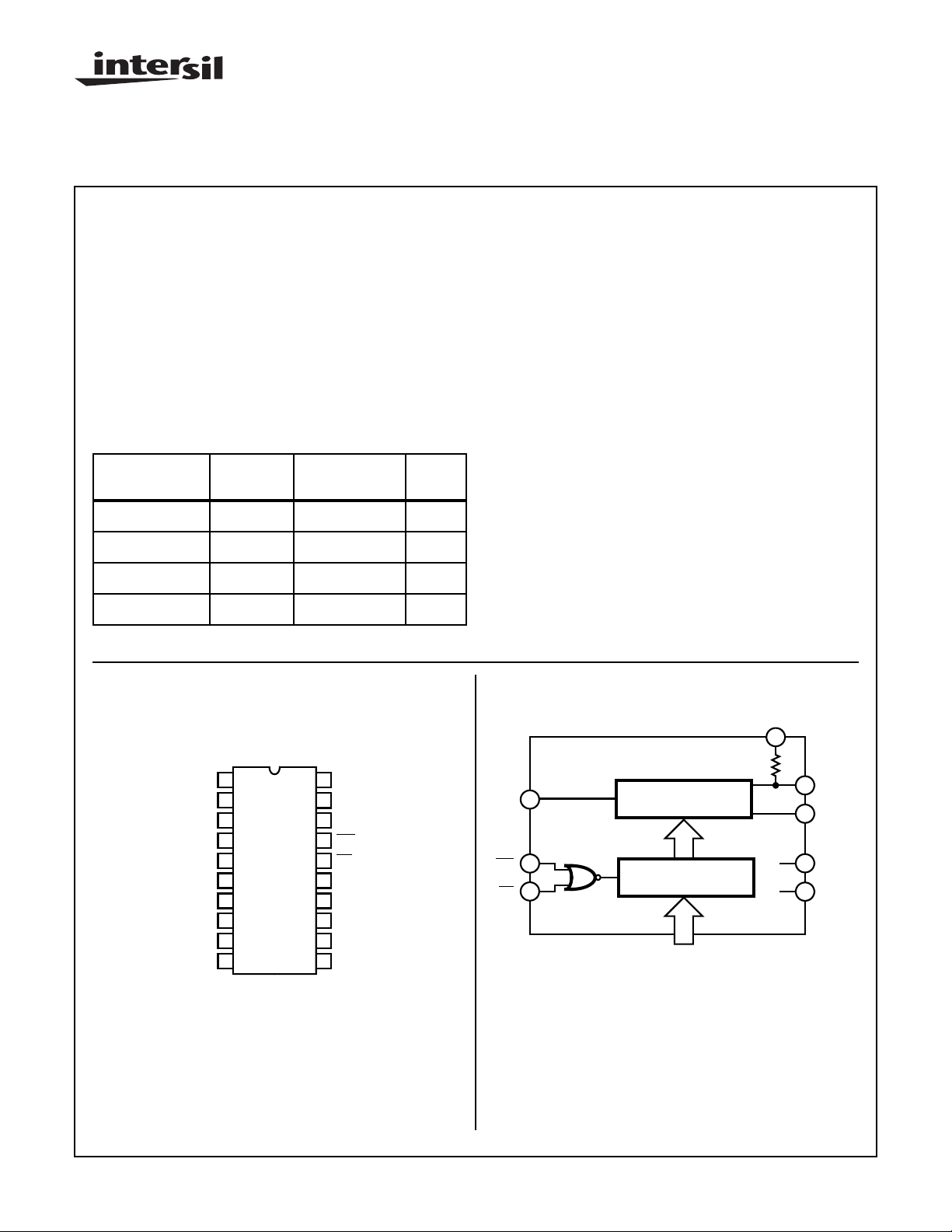
AD7545JN 0 to 70 20 Ld PDIP E20.3
AD7545KN 0 to 70 20 Ld PDIP E20.3
AD7545AN -40 to 85 20 Ld PDIP E20.3
AD7545BN -40 to 85 20 Ld PDIP E20.3
RANGE (oC) PACKAGE
12-Bit, Buffered, Multiplying CMOS DAC
Description
The AD7545 is a low cost monolithic 12-bit, CMOS
multiplying DAC with on-board data latches. Data is loaded
in a single 12-bit wide word which allows interfacing directly
to most 12-bit and 16-bit bus systems. Loading of the input
latches is under the control of the CS and WR inputs. A logic
low on these control inputs makes the input latches transparent allowing direct unbuffered operation of the DAC.
PKG.
NO.
Pinout
OUT 1
AGND
DGND
DB11 (MSB)
DB10
DB9
DB8
DB7
DB6
DB5
1
2
3
4
5
6
7
8
9
10
AD7545
(PDIP)
TOP VIEW
R
20
V
19
V
18
WR
17
CS
16
DB0 (LSB)
15
DB1
14
DB2
13
12
DB3
11
DB4
FB
REF
DD
Functional Diagram
AD7545
V
REF
WR
CS
19
17
16
MULTIPLYING DAC
INPUT DATA LATCHES
12-BIT
12
12
DB11 - DB0
(PINS 4 - 15)
R
FB
20
R
1
OUT1
2
AGND
18
V
DD
3
DGND
CAUTION: These devices are sensitive to electrostatic discharge; follow proper IC Handling Procedures.
http://www.intersil.com or 407-727-9207
| Copyright © Intersil Corporation 1999
10-10
File Number 3108.1

AD7545
Absolute Maximum Ratings Thermal Information
Supply Voltage (VDD to DGND) . . . . . . . . . . . . . . . . . . . -0.3V, +17V
Digital Input Voltage to DGND . . . . . . . . . . . . . . . .-0.3V, VDD +0.3V
V
, V
to DGND . . . . . . . . . . . . . . . . . . . . . . . . . . . . . . . ±25V
REF
to DGND . . . . . . . . . . . . . . . . . . . . . . . . . . .-0.3V, VDD +0.3V
V
RFB
PIN1
AGND to DGND . . . . . . . . . . . . . . . . . . . . . . . . . . .-0.3V, VDD +0.3V
Operating Conditions
Temperature Ranges
Commercial (J, K, Grades) . . . . . . . . . . . . . . . . . . . . .0oC to 70oC
Industrial (A, B, Grades) . . . . . . . . . . . . . . . . . . . . . -40oC to 85oC
Extended (S Grades) . . . . . . . . . . . . . . . . . . . . . . -55oC to 125oC
CAUTION: Stresses above those listed in “Absolute Maximum Ratings” may cause permanent damage to the device. This is a stress only rating and operation
of the device at these or any other conditions above those indicated in the operational sections of this specification is not implied.
NOTE:
1. θJA is measured with the component mounted on an evaluation PC board in free air.
Thermal Resistance (Typical, Note 1) θJA (oC/W)
PDIP Package. . . . . . . . . . . . . . . . . . . . . . . . . . . . . 125
Maximum Junction Temperature (PDIP Package) . . . . . . . . .150oC
Maximum Storage Temperature Range . . . . . . . . . .-65oC to 150oC
Maximum Lead Temperature (Soldering 10s). . . . . . . . . . . . 300oC
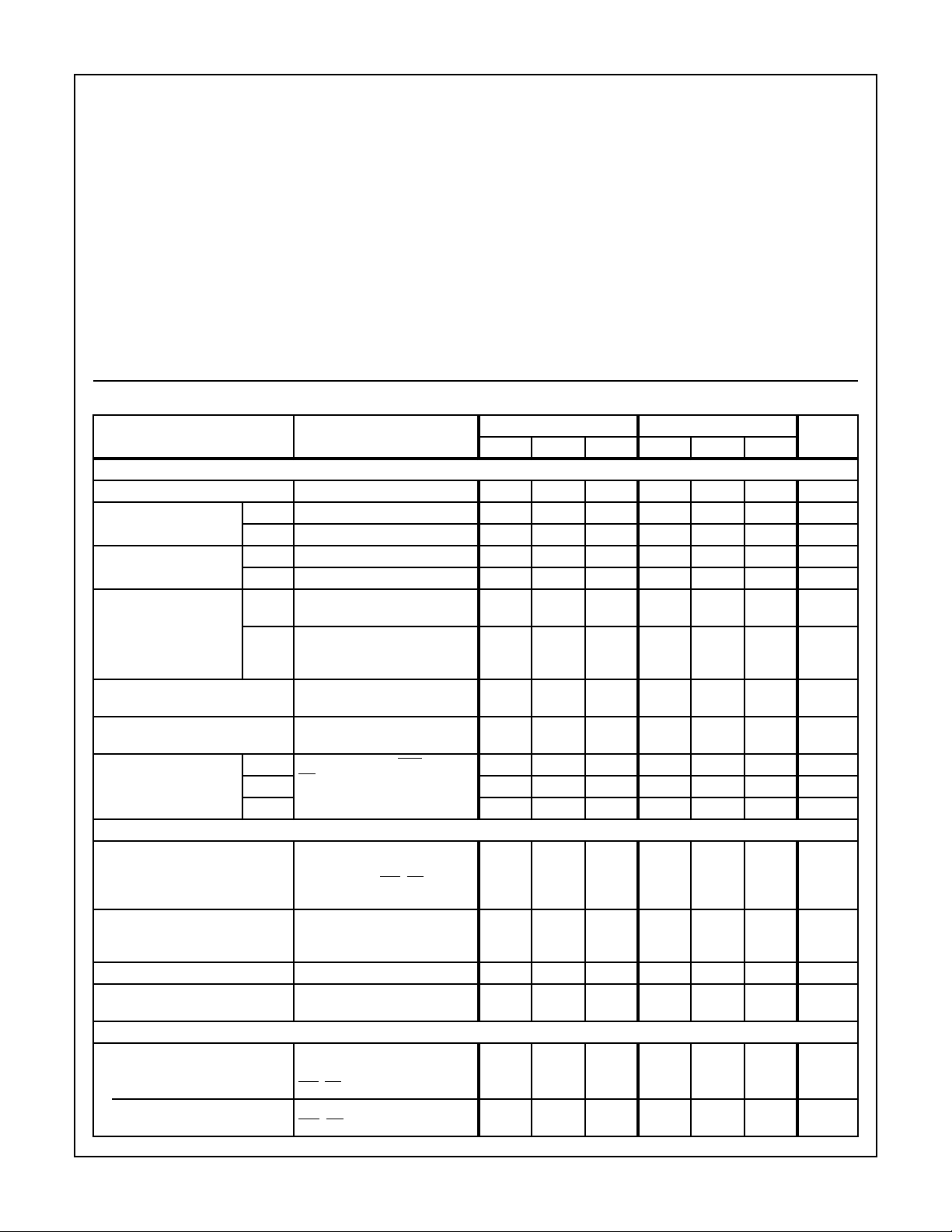
Electrical Specifications T
= See Note 2, V
A
= +10V, V
REF
= 0V, AGND = DGND, Unless Otherwise Specified
OUT1
VDD = +5V VDD = +15V
PARAMETER TEST CONDITIONS
UNITSMIN TYP MAX MIN TYP MAX
STATIC PERFORMANCE
Resolution 12 12 Bits
Relative Accuracy J, A, S - - ±2- -±2 LSB
K, B - - ±1- -±1 LSB
Differential Nonlinearity J, A, S 10-Bit Monotonic T
K, B 12-Bit Monotonic T
Gain Error
(Using Internal RFB)
J, A, S DAC Register Loaded with
1111 1111 1111
K, B Gain Error is Adjustable
MIN
MIN
to T
to T
MAX
MAX
--±4- -±4 LSB
--±1- -±1 LSB
--±20 - - ±25 LSB
--±10 - - ±15 LSB
Using the Circuits of
Figures 4 and 5 (Note 3)
Gain Temperature Coefficient
∆Gain/∆Temperature
DC Supply Rejection
∆Gain/∆V
DD
Output Leakage Current
at OUT1
Typical Value is 2ppm/oC for
--±5- -±10 ppm/oC
VDD = +5V (Note 4)
∆VDD = ±5% 0.015 - 0.03 0.01 - 0.02 %
J, K DB0 - DB11 = 0V; WR,
CS = 0V (Note 2)
A, B - -50- -50nA
- - 50 - - 50 nA
S - - 200 - - 200 nA
DYNAMIC CHARACTERISTICS
Current Setting Time To1/2 LSB, OUT1 LOAD = 100Ω,
--2--2µs
DAC Output Measured from
Falling Edge ofWR, CS = 0V
(Note 4)
Propagation Delay from Digital Input
Change to 90% of Final Analog
OUT1 LOAD = 100Ω,
C
= 13pF (Notes 4 and 5)
EXT
- - 300 - - 250 ns
Output
Digital to Analog Glitch Impulse V
AC Feedthrough at OUT1 V
= AGND - 400 - - 250 - nV/s
REF
= ±10V, 10kHz Sinewa v e
REF
-5--5-mV
(Note 6)
ANALOG OUTPUTS
Output Capacitance
C
OUT1
DB0 - DB11 = 0V,
- - 70 - - 70 pF
WR, CS = 0 V(Note 4)
C
OUT1
DB0 - DB11 = VDD,
- - 200 - - 200 pF
WR, CS = 0V (Note 4)
P-P
10-11

AD7545
Electrical Specifications T
= See Note 2, V
A
REF
= +10V, V
= 0V, AGND = DGND, Unless Otherwise Specified (Continued)
OUT1
VDD = +5V VDD = +15V
PARAMETER TEST CONDITIONS
UNITSMIN TYP MAX MIN TYP MAX
REFERENCE INPUT
Input Resistance (Pin 19 to GND) Input Resistance
7--7--kΩ
TC = -300ppm/oC (Typ)
Typical Input Resistance = 11kΩ - - 25 - - 25 kΩ
DIGITAL INPUTS
Input High Voltage, V
Input Low Voltage, V
Input Current, I
IN
IH
IL
VIN = 0 or VDD (Note 7) ±1-±10 ±1-±10 µA (Max)
2.4 - - - - 13.5 V
- - 0.8 - - 1.5 V
Input Capacitance
DB0 - DB11 VIN = 0 (Note 4) - - 7 - - 7 pF
WR, CS VIN = 0 (Note 4) - - 20 - - 20 pF
SWITCHING CHARACTERISTICS (Note 4)
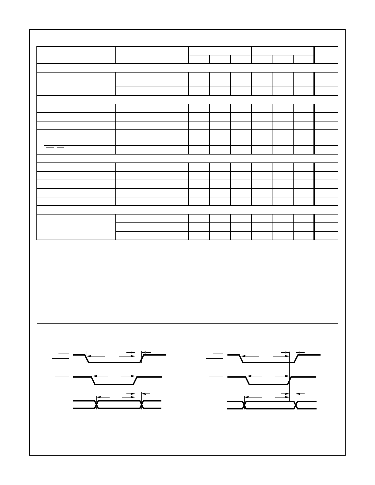
Chip Select to Write Setup Time, tCSSee Figure 1 380 200 - 200 120 - ns
Chip Select to Write Hold Time, tCHSee Figure 1 0 - - 0 - - ns
Write Pulse Width, t
Data Setup Time, t
Data Hold Time, t
DH
WR
DS
tCS≥ tWR, tCH≥ 0, See Figure 1 400 175 - 240 100 ns
See Figure 1 210 100 - 120 60 - ns
See Figure 1 10 - - 10 - - ns
POWER SUPPLY CHARACTERISTICS
I
DD
All Digital Inputs VIL or V
All Digital Inputs 0V or V
All Digital Inputs 0V or V
IH
DD
DD
--2--2mA
- 100 500 - 100 500 µA
-10- -10- µA
NOTES:
2. Temperature Ranges as follows: J, K versions: 0oC to 70oC
A, B versions: -20oC to 85oC
S version: -55oC to 125oC
TA = 25oC for TYP Specifications. MIN and MAX are measured over the specified operating range.
3. This includes the effect of 5ppm maximum gain TC.
4. Parameter not tested. Parameter guaranteed by design, simulation, or characterization.
5. DB0 - DB11 = 0V to VDD or VDD to 0V in plastic and sidebraze package.
6. Feedthrough can be further reduced by connecting the metal lid on the ceramic package to DGND.
7. Logic inputs are MOS gates. Typical input current (25oC) is less than 1nA.
8. Typical values are not guaranteed but reflect mean performance specification.
Specifications subject to change without notice.
Timing Diagrams
CHIP
SELECT
WRITE
DATA IN
(DB0 - DB11)
FIGURE 1A. TYPICAL WRITE CYCLE FIGURE 1B. PREFERRED WRITE CYCLE
t
CS
t
WR
t
DS
DATA VALID
t
CH
V
DD
0
V
DD
t
DH
0
V
DD
0
CHIP
SELECT
WRITE
DATA IN
(DB0 - DB11)
FIGURE 1. WRITE CYCLE TIMING DIAGRAM
10-12
t
CS
t
WR
t
DS
DATA VALID
t
CH
V
DD
0
V
DD
t
DH
0
V
DD
0
 Loading...