Intersil Corporation AD7533 Datasheet

AD7523, AD7533
August 1997
Features
• 8-Bit, 9-Bit and 10-Bit Linearity
• Low Gain and Linearity Temperature Coefficients
• Full Temperature Range Operation
• Static Discharge Input Protection
• TTL/CMOS Compatible
• Supply Range. . . . . . . . . . . . . . . . . . . . . . . .+5V to +15V
• Fast Settling Time at 25
• Four Quadrant Multiplication
• AD7533 Direct AD7520 Equivalent
o
C . . . . . . . . . . . . 150ns (Max)
Description
The AD7523 and AD7533 are monolithic, low cost, high
performance, 8-bit and 10-bit accurate, multiplying digital-toanalog converter (DAC), in a 16 pin DIP.
Intersil’ thin film resistors on CMOS circuitry provide 10-bit
resolution (8-bit, 9-bit and 10-bit accuracy), with TTL/CMOS
compatible operation.
The AD7523 and AD7533s accurate four quadrant
multiplication, full military temperature range operation, full
input protection from damage due to static discharge by
clamps to V+ and GND, and very low power dissipation
make it a very versatile converter.
Low noise audio gain controls, motor speed controls,
digitally controlled gain and digital attenuators are a few of
8-Bit, Multiplying D/A Converters
the wide range of applications of the AD7523 and AD7533.
Ordering Information
PART NUMBER LINEARITY (INL, DNL) TEMP. RANGE (oC) PACKAGE PKG. NO.
AD7523JN, AD7533JN 0.2% (8-Bit) 0 to 70 16 Ld PDIP E16.3
AD7523KN, AD7533KN 0.1% (9-Bit) 0 to 70 16 Ld PDIP E16.3
AD7523LN, AD7533LN 0.05% (10-Bit) 0 to 70 16 Ld PDIP E16.3
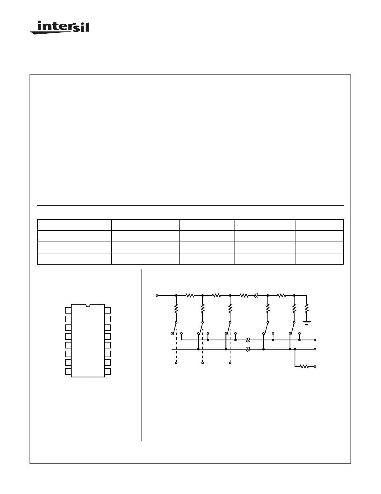
Pinout
AD7523, AD7533
(PDIP)
TOP VIEW
1
I
OUT1
2
I
OUT2
3
GND
BIT 2
BIT 3
BIT 4
BIT 5
4
5
6
7
8
BIT 1 (MSB)
NOTE:
1. NC for AD7523 only.
16
R
15
V
14
V+
NC/BIT 10
13
(NOTE 1)
NC/BIT 9
12
(NOTE 1)
BIT 8
11
10
BIT 7
9
BIT 6
FEEDBACK
REF IN
Functional Block Diagram
V
REF IN
(15)
SPDT
NMOS
SWITCHES
NOTE: Switches shown for digital inputs “High”
10kΩ 10kΩ 10kΩ 10kΩ
MSB
(4)
(5) (6)
BIT 3BIT 2
20kΩ20kΩ20kΩ20kΩ20kΩ
10kΩ
20kΩ
(3)
I
(2)
OUT2
I
(1)
OUT1
R
FEEDBACK
(16)
CAUTION: These devices are sensitive to electrostatic discharge; follow proper IC Handling Procedures.
http://www.intersil.com or 407-727-9207
| Copyright © Intersil Corporation 1999
10-8
File Number 3105.1

AD7523, AD7533
Absolute Maximum Ratings Thermal Information
Supply Voltage (V+ to GND). . . . . . . . . . . . . . . . . . . . . . . . . . . +17V
V
. . . . . . . . . . . . . . . . . . . . . . . . . . . . . . . . . . . . . . . . . . . . . ±25V
REF
Digital Input Voltage Range . . . . . . . . . . . . . . . . . . . . . . .V+ to GND
Output Voltage Compliance . . . . . . . . . . . . . . . . . . . . -100mV to V+
Operating Conditions
Temperature Range
JN, KN, LN Versions. . . . . . . . . . . . . . . . . . . . . . . . . .0oC to 70oC
CAUTION: Stresses above those listed in “Absolute Maximum Ratings” may cause permanent damage to the device. This is a stress only rating and operation
of the device at these or any other conditions above those indicated in the operational sections of this specification is not implied.
NOTE:
1. θJA is measured with the component mounted on an evaluation PC board in free air.
Thermal Resistance (Typical, Note 1) θJA (oC/W)
PDIP Package. . . . . . . . . . . . . . . . . . . . . . . . . . . . . . . . . . 100
Maximum Junction Temperature (Plastic Package) . . . . . . . . 150oC
Maximum Storage Temperature . . . . . . . . . . . . . . . .-65oC to 150oC
Maximum Lead Temperature (Soldering 10s) . . . . . . . . . . . . . 300oC
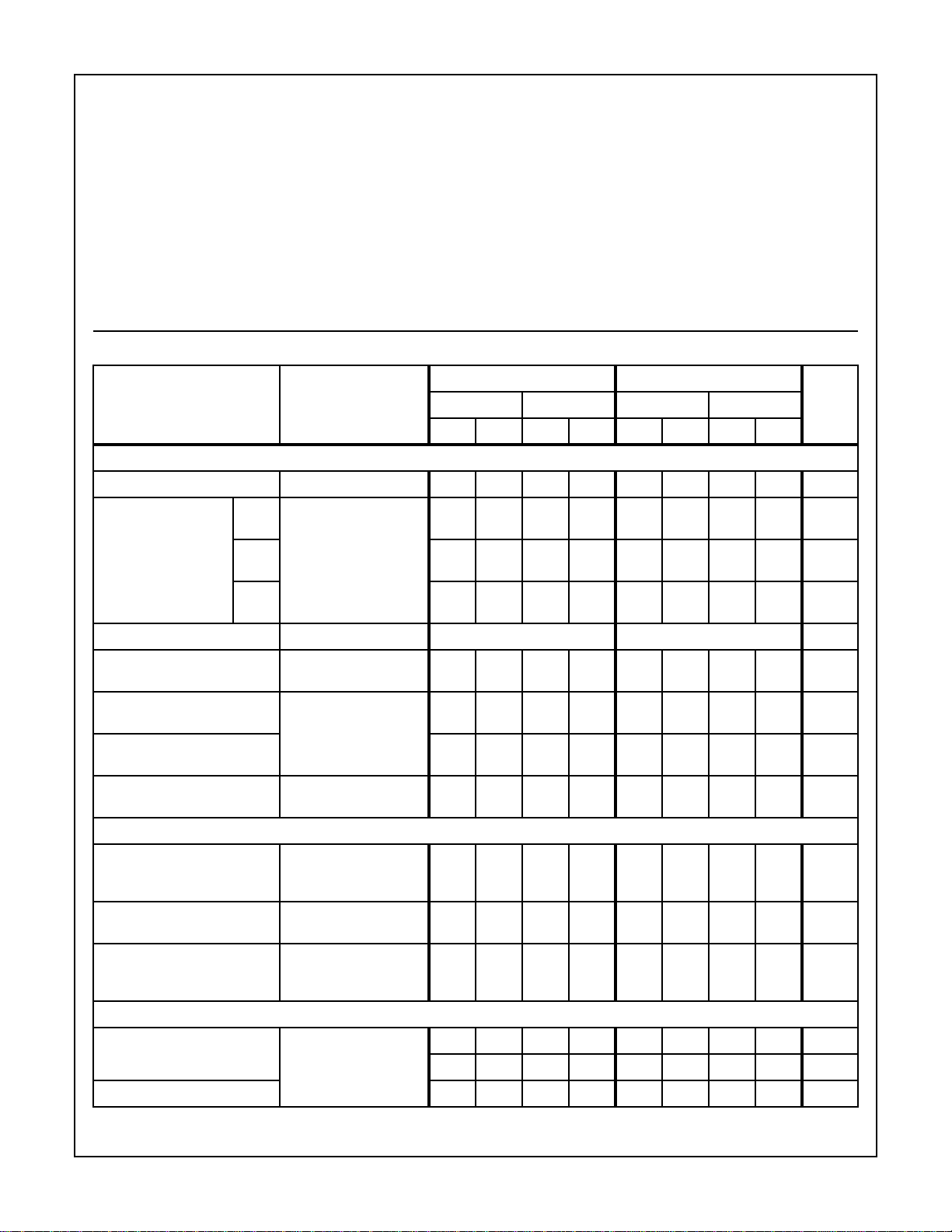
Electrical Specifications V+ = +15V, V
= +10V, V
REF
OUT1
= V
= 0V, Unless Otherwise Specified
OUT2
AD7523 AD7533
TA 25oCTA MIN-MAX TA 25oCTA MIN-MAX
PARAMETER TEST CONDITIONS
MIN MAX MIN MAX MIN MAX MIN MAX
UNITS
SYSTEM PERFORMANCE
Resolution 8 - 8 - 10 - 10 - Bits
Nonlinearity J -10V ≤ V
V
OUT1
K, T - ±0.1 - ±0.1 - ±0.1 - ±0.1 % of
(Notes 2, 3, 6)
= V
REF
≤ +10V
OUT2
= 0V
- ±0.2 - ±0.2 - ±0.2 - ±0.2 % of
FSR
FSR
L-±0.05 - ±0.05 - ±0.05 - ±0.05 % of
FSR
Monotonicity Guaranteed Guaranteed
Gain Error All Digital Inputs High
(Note 3)
Nonlinearity Tempco -10V ≤ V
REF
≤ + 10V
(Notes 3, 4)
- ±1.5 - ±1.8 - ±1.4 - ±1.8 % of
FSR
- ±2-±2-±2-±2 ppm of
FSR/oC
Gain Error Tempco - ±10 - ±10 - ±10 - ±10 ppm of
FSR/oC
Output Leakage Current
V
OUT1
= V
= 0 - ±50 - ±200 - ±50 - ±200 nA
OUT2
(Either Output)
DYNAMIC CHARACTERISTICS
Power Supply Rejection V+ = 14.0V to 15.0V
(Note 3)
- ±0.02 - ±0.03 - ±0.005 - ±0.008 % of
FSR/%
of ∆V+
Output Current Settling Time To 0.2% of FSR,
- 150 - 200 - 600 - 800 ns
RL = 100Ω (Note 4)
Feedthrough Error V
REF
= 20V
P-P
, 200kHz
- ±1/2 - ±1-±0.05 - ±0.1 LSB
Sine Wave, All Digital
Inputs Low (Note 4)
REFERENCE INPUTS
Input Resistance (Pin 15) All Digital Inputs High
I
at Ground (Note 4)
OUT1
5-5-5-5-kΩ
- 20 - 20 - 20 - 20 kΩ
Temperature Coefficient - -500 - -500 - -300 - -300 ppm/οC
10-9

AD7523, AD7533
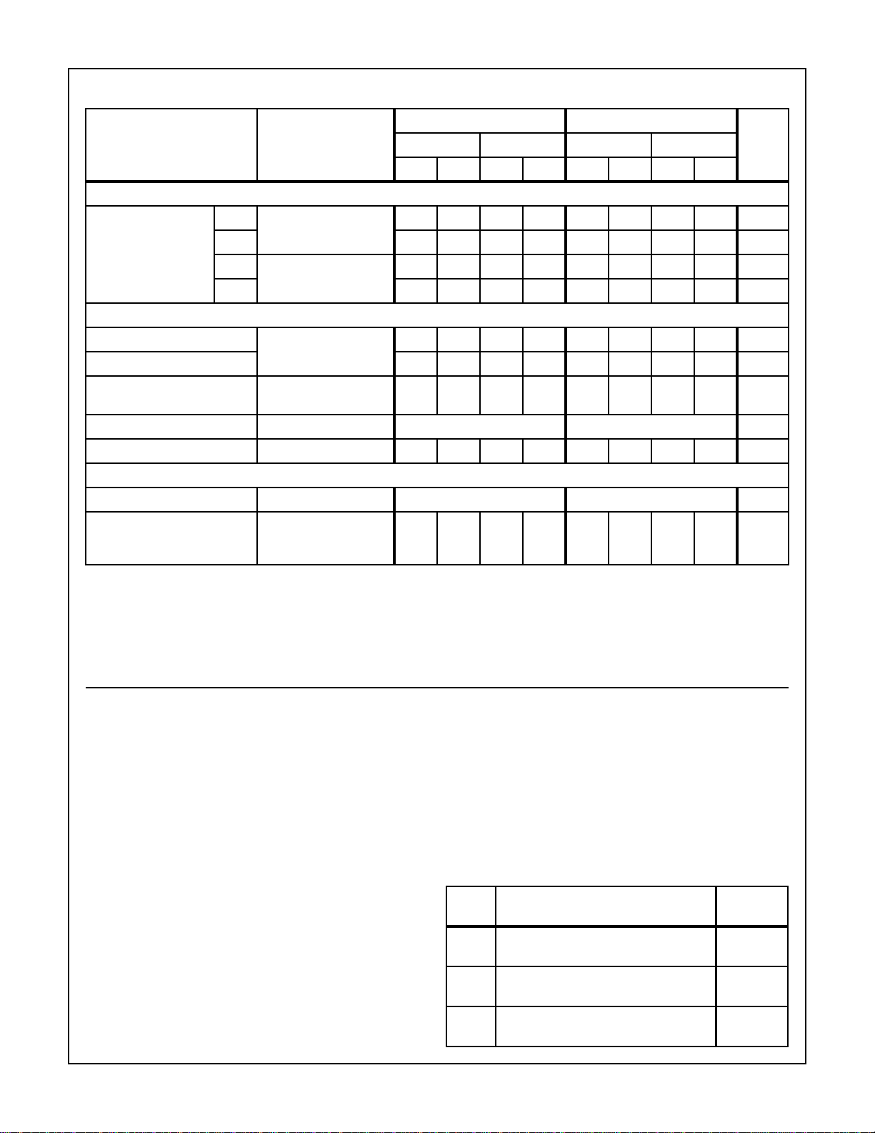
Electrical Specifications V+ = +15V, V
PARAMETER TEST CONDITIONS
ANALOG OUTPUT
Output Capacitance C
C
C
C
DIGITAL INPUTS
Low State Threshold, V
High State Threshold, V
Input Current (Low or High),
IIL, I
IH
Input Coding See Tables 1 and 3 Binary/Offset Binary Binary/Offset Binary
Input Capacitance (Note 4) - 4 - 4 - 4 - 4 pF
POWER SUPPLY CHARACTERISTICS
Power Supply Voltage Range (Note 6) +5 to +16 +5 to +16 V
I+ All Digital Inputs High or
NOTES:
2. Full Scale Range (FSR) is 10V for unipolar and ±10V for bipolar modes.
3. Using internal feedback resistor, R
4. Guaranteed by design or characterization and not production tested.
5. Accuracy not guaranteed unless outputs at ground potential.
6. Accuracy is tested and guaranteed at V+ = +15V, only.
IL
IH
All Digital Inputs High
OUT1
(Note 4)
OUT2
All Digital Inputs Low
OUT1
(Note 4)
OUT2
VIN = 0V or + 15V - ±1-±1-±1-±1 µA
Low (Excluding Ladder
Network)
FEEDBACK
= +10V, V
REF
.
= V
OUT1
TA 25oCTA MIN-MAX TA 25oCTA MIN-MAX
MIN MAX MIN MAX MIN MAX MIN MAX
- 100 - 100 - 100 - 100 pF
- 30 - 30 - 35 - 35 pF
- 30 - 30 - 35 - 35 pF
- 100 - 100 - 100 - 100 pF
- 0.8 - 0.8 - 0.8 - 0.8 V
2,4 - 2,4 - 2.4 - 2.4 - V
- 2 - 2.5 - 2 - 2.5 mA
= 0V, Unless Otherwise Specified (Continued)
OUT2
AD7523 AD7533
UNITS
Definition of Terms
Nonlinearity: Error contributed by deviation of the DAC
transfer function from a “best straight line” through the actual
plot of transfer function. Normally expressed as a
percentage of full scale range or in (sub)multiples of 1 LSB.
Resolution: It is addressing the smallest distinct analog
output change that a D/A converter can produce. It is
commonly expressed as the number of converter bits. A
converter with resolution of n bits can resolve output changes
-N
of 2
of the full-scale range, e.g., 2-N V
conversion. Resolution by no means implies linearity.
Settling Time: Time required for the output of a DAC to
settle to within specified error band around its final value
1
(e.g.,
/2 LSB) for a given digital input change, i.e., all digital
inputs LOW to HIGH and HIGH to LOW.
Gain Error: The difference between actual and ideal analog
output values at full-scale range, i.e., all digital inputs at
HIGH state. It is expressed as a percentage of full scale
range or in (sub)multiples of 1 LSB.
for a unipolar
REF
Feedthrough Error: Error caused by capacitive coupling
from V
Output Capacitance: Capacitance from I
REF
to I
with all digital inputs LOW.
OUT1
OUT1
, and I
terminals to ground.
Output Leakage Current: Current which appears on
, terminal when all digital inputs are LOW or on I
I
OUT1
terminal when all digital inputs are HIGH.
For further information on the use of this device, see the
following Application Notes:
AnswerFAX
NOTE # DESCRIPTION
AN002 “Principles of Data Acquisition and
Conversion”
AN018 “Do’s and Don’ts of Applying A/D
Converters”
AN042 “Interpretation of Data Conversion
Accuracy Specifications”
10-10
OUT2
OUT2
DOC. #
9002
9018
9042
 Loading...