Intersil Corporation AD7521, AD7520, AD7531, AD7530 Datasheet

AD7520, AD7530,
AD7521, AD7531
August 1997
Features
• AD7520/AD7530, 10-Bit Resolution; 8-Bit, 9-Bit and
10-Bit Linearity
• AD7521/AD7531, 12-Bit Resolution; 8-Bit, 9-Bit and
10-Bit Linearity
• Low Power Dissipation (Max). . . . . . . . . . . . . . . .20mW
• Low Nonlinearity Tempco at 2ppm of FSR/
• Current Settling Time to 0.05% of FSR . . . . . . . . 1.0µs
• Supply Voltage Range . . . . . . . . . . . . . . . . ±5V to +15V
o
C
10-Bit, 12-Bit, Multiplying D/A Converters
Description
The AD7520/AD7530 and AD7521/AD7531 are monolithic,
high accuracy, low cost 10-bit and 12-bit resolution,
multiplying digital-to-analog converters (DAC). Intersil’
thin-film on CMOS processing gives up to 10-bit accuracy
with TTL/CMOS compatible operation. Digital inputs are fully
protected against static discharge by diodes to ground and
positive supply.
Typical applications include digital/analog interfacing,
multiplication and division, programmable power supplies,
CRT character generation, digitally controlled gain circuits,
integrators and attenuators, etc.
• TTL/CMOS Compatible
The AD7530 and AD7531 are identical to the AD7520 and
• Full Input Static Protection
• /883B Processed Versions Available
AD7521, respectively, with the exception of output leakage
current and feedthrough specifications.
Ordering Information
PART NUMBER LINEARITY (INL, DNL) TEMP. RANGE (oC) PACKAGE PKG. NO.
AD7520JN, AD7530JN 0.2% (8-Bit) 0 to 70 16 Ld PDIP E16.3
AD7520KN, AD7530KN 0.1% (9-Bit) 0 to 70 16 Ld PDIP E16.3
AD7521JN, AD7531JN 0.2% (8-Bit) 0 to 70 18 Ld PDIP E18.3
AD7521KN, AD7531KN 0.1% (9-Bit) 0 to 70 18 Ld PDIP E18.3
AD7520LN, AD7530LN 0.05% (10-Bit) -40 to 85 16 Ld PDIP E16.3
AD7521LN, AD7531LN 0.05% (10-Bit) -40 to 85 18 Ld PDIP E18.3
AD7520JD 0.2% (8-Bit) -25 to 85 16 Ld CERDIP F16.3
AD7520KD 0.1% (9-Bit) -25 to 85 16 Ld CERDIP F16.3
AD7520LD 0.05% (10-Bit) -25 to 85 16 Ld CERDIP F16.3
AD7520SD, AD7520SD/883B 0.2% (8-Bit) -55 to 125 16 Ld CERDIP F16.3
AD7520UD, AD7520UD/883B 0.05% (10-Bit) -55 to 125 16 Ld CERDIP F16.3
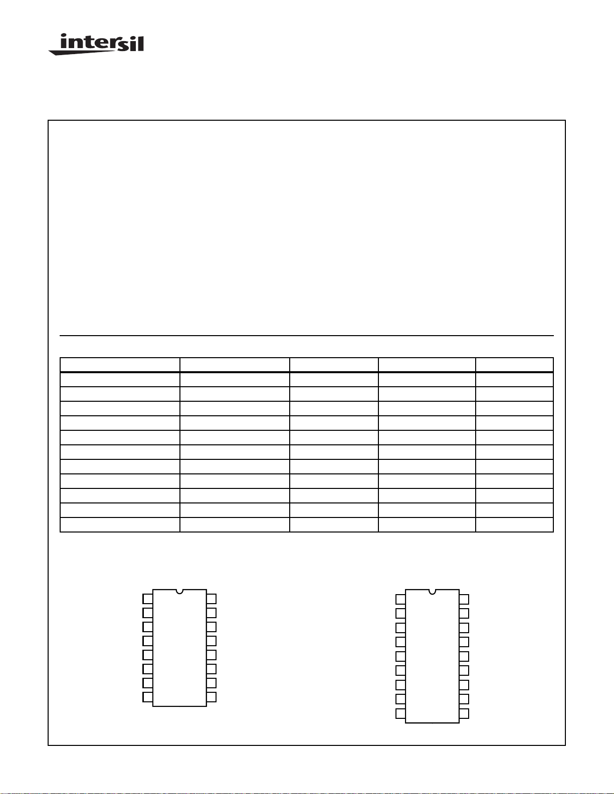
Pinouts
AD7520, AD7530
(CERDIP, PDIP)
TOP VIEW
16
1
I
OUT1
2
I
OUT2
3
GND
BIT 2
BIT 3
BIT 4
BIT 5
4
5
6
7
8
| Copyright © Intersil Corporation 1999
BIT 1 (MSB)
CAUTION: These devices are sensitive to electrostatic discharge; follow proper IC Handling Procedures.
http://www.intersil.com or 407-727-9207
R
FEEDBACK
15
V
REF
14
V+
13
BIT 10 (LSB)
12
BIT 9
BIT 8
11
10
BIT 7
9
BIT 6
BIT 1 (MSB)
10-7
I
OUT1
I
OUT2
GND
BIT 2
BIT 3
BIT 4
BIT 5
BIT 6
1
2
3
4
5
6
7
8
9
AD7521, AD7531
(PDIP)
TOP VIEW
18
R
FEEDBACK
V
17
REF
16
V+
15
BIT 12 (LSB)
14
BIT 11
13
BIT 10
12
BIT 9
11
BIT 8
10
BIT 7
File Number 3104.1

AD7520, AD7530, AD7521, AD7531
Absolute Maximum Ratings Thermal Information
Supply Voltage (V+ to GND). . . . . . . . . . . . . . . . . . . . . . . . . . . +17V
V
. . . . . . . . . . . . . . . . . . . . . . . . . . . . . . . . . . . . . . . . . . . . . ±25V
REF
Digital Input Voltage Range . . . . . . . . . . . . . . . . . . . . . . .V+ to GND
Output Voltage Compliance . . . . . . . . . . . . . . . . . . . . -100mV to V+
Operating Conditions
Temperature Ranges
JN, KN, LN Versions. . . . . . . . . . . . . . . . . . . . . . . . . .0oC to 70oC
JD, KD, LD Versions . . . . . . . . . . . . . . . . . . . . . . . . -25oC to 85oC
SD, UD Versions. . . . . . . . . . . . . . . . . . . . . . . . . . -55oC to 125oC
CAUTION: Stresses above those listed in “Absolute Maximum Ratings” may cause permanent damage to the device. This is a stress only rating and operation
of the device at these or any other conditions above those indicated in the operational sections of this specification is not implied.
The digital control inputs are zener protected; however, permanent damage may occur on unconnected units under high energy electrostatic fields. Keep
unused units in conductive foam at all times.
Do not apply voltages higher than VDD or less than GND potential on any terminal except V
NOTE:
1. θJA is measured with the component mounted on an evaluation PC board in free air.
Thermal Resistance (Typical, Note 1) θJA (oC/W) θJC (oC/W)
16 Ld PDIP Package. . . . . . . . . . . . . . . . 100 N/A
18 Ld PDIP Package. . . . . . . . . . . . . . . . 90 N/A
CERDIP Package . . . . . . . . . . . . . . . . . . 75 20
Maximum Junction Temperature (Hermetic Package) . . . . . . . . 175oC
Maximum Junction Temperature (Plastic Packages) . . . . . . .150oC
Maximum Storage Temperature Range . . . . . . . . . .-65oC to 150oC
Maximum Lead Temperature (Soldering 10s). . . . . . . . . . . . . 300oC
REF
and R
FEEDBACK
.
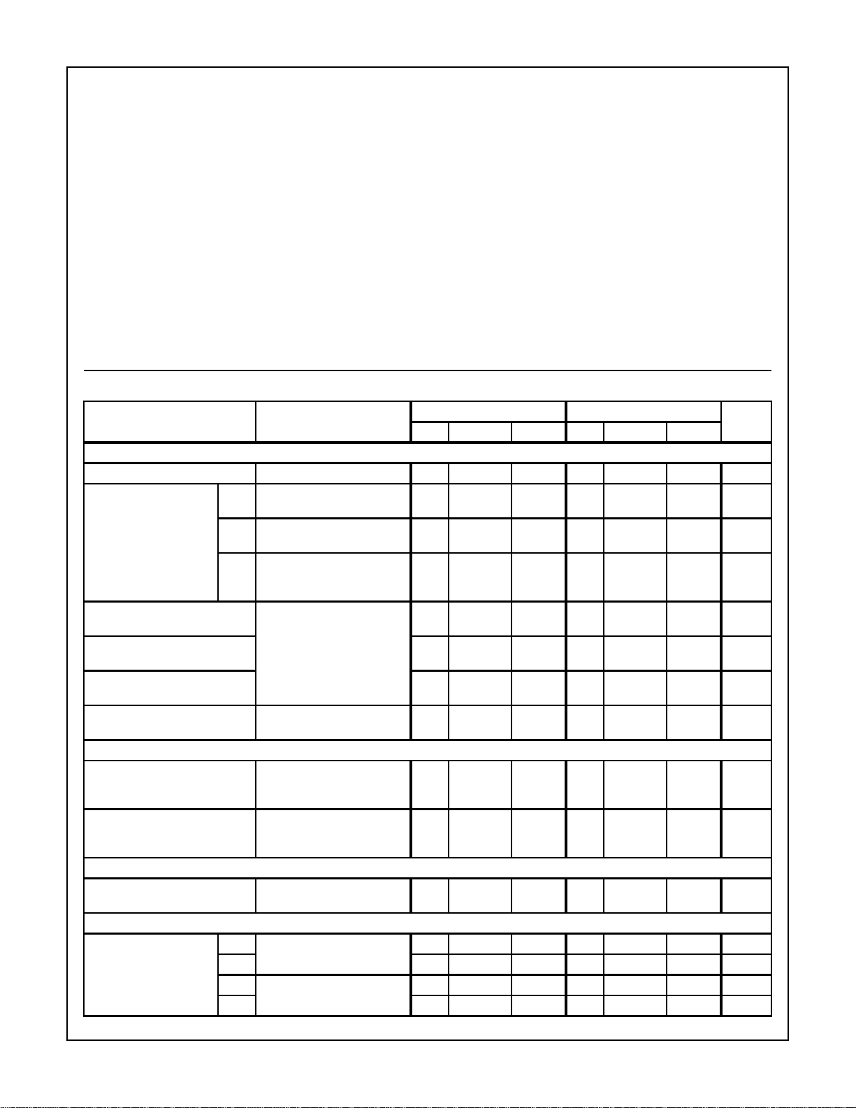
Electrical Specifications V+ = +15V, V
= +10V, TA = 25oC Unless Otherwise Specified
REF
AD7520/AD7530 AD7521/AD7531
PARAMETER TEST CONDITIONS
UNITSMIN TYP MAX MIN TYP MAX
SYSTEM PERFORMANCE (Note 2)
Resolution 10 10 10 12 12 12 Bits
Nonlinearity J, S S Over -55oC to 125oC
(Notes 2, 5) (Figure 3)
o
K T Over -55
C to 125oC
(Figure 2)
L, U -10V ≤ V
REF
≤ +10V
U Over -55oC to 125oC
--±0.2
(8-Bit)
--±0.1
(9-Bit)
--±0.05
(10-Bit)
--±0.2
(8-Bit)
--±0.1
(9-Bit)
--±0.05
(10-Bit)
% of
FSR
% of
FSR
% of
FSR
(Figure 2)
Nonlinearity Tempco -10V ≤ V
(Notes 3, 4)
REF
≤ +10V
-- ±2- - ±2 ppm of
FSR/oC
Gain Error - ±0.3 - - ±0.3 - % of
FSR
Gain Error Tempco - - ±10 - - ±10 ppm of
FSR/
Output Leakage Current
(Either Output)
Over the Specified
Temperature Range
--±200
(±300)
--±200
(±300)
nA
DYNAMIC CHARACTERISTICS
Output Current Settling Time To 0.05% of FSR (All Digital
- 1.0 - - 1.0 - µs
Inputs Low To High And High
To Low) (Note 4) (Figure 7)
Feedthrough Error V
REF
= 20V
P-P
, 10kHz
- - 10 - - 10 mV
(50kHz) All Digital Inputs Low
(Note 4) (Figure 6)
REFERENCE INPUT
Input Resistance All Digital Inputs High
at Ground
I
OUT1
5 10 20 5 10 20 kΩ
ANALOG OUTPUT
Output Capacitance I
All Digital Inputs High
OUT1
(Note 4) (Figure 5)
I
OUT2
All Digital Inputs Low
I
OUT1
(Note 4) (Figure 5)
I
OUT2
- 200 - - 200 - pF
-75 --75 - pF
-75 --75 - pF
- 200 - - 200 - pF
P-P
o
C
10-8

AD7520, AD7530, AD7521, AD7531
Electrical Specifications V+ = +15V, V
= +10V, TA = 25oC Unless Otherwise Specified (Continued)
REF
AD7520/AD7530 AD7521/AD7531
PARAMETER TEST CONDITIONS
Output Noise Both Outputs
(Note 4) (Figure 4)
- Equivalent
to 10kΩ
- - Equivalent
to 10kΩ
UNITSMIN TYP MAX MIN TYP MAX
- Johnson
Noise
DIGITAL INPUTS
Low State Threshold, V
High State Threshold, V
Input Current, I
, I
IL
IH
IL
IH
Over the Specified
Temperature Range
VIN = 0V or +15V
- - 0.8 - - 0.8 V
2.4 - - 2.4 - - V
-- ±1- - ±1 µA
Input Coding See Tables 1 and 2 Binary/Offset Binary
POWER SUPPLY CHARACTERISTICS
Power Supply Rejection V+ = 14.5V to 15.5V
(Note 3) (Figure 3)
- ±0.005 - - ±0.005 - % FSR/
% ∆V+
Power Supply Voltage Range +5 to +15 +5 to +15 V
I+ All Digital Inputs at 0V or V+
- ±1--±1-µA
Excluding Ladder Network
All Digital Inputs High or Low
-- 2-- 2mA
Excluding Ladder Network
Total Power Dissipation Including the Ladder Network - 20 - - 20 - mW
NOTES:
2. Full scale range (FSR) is 10V for Unipolar and±10V for Bipolar modes.
3. Using internal feedback resistor R
FEEDBACK
.
4. Guaranteed by design, or characterization and not production tested.
5. Accuracy not guaranteed unless outputs at GND potential.
6. Accuracy is tested and guaranteed at V+ = 15V only.
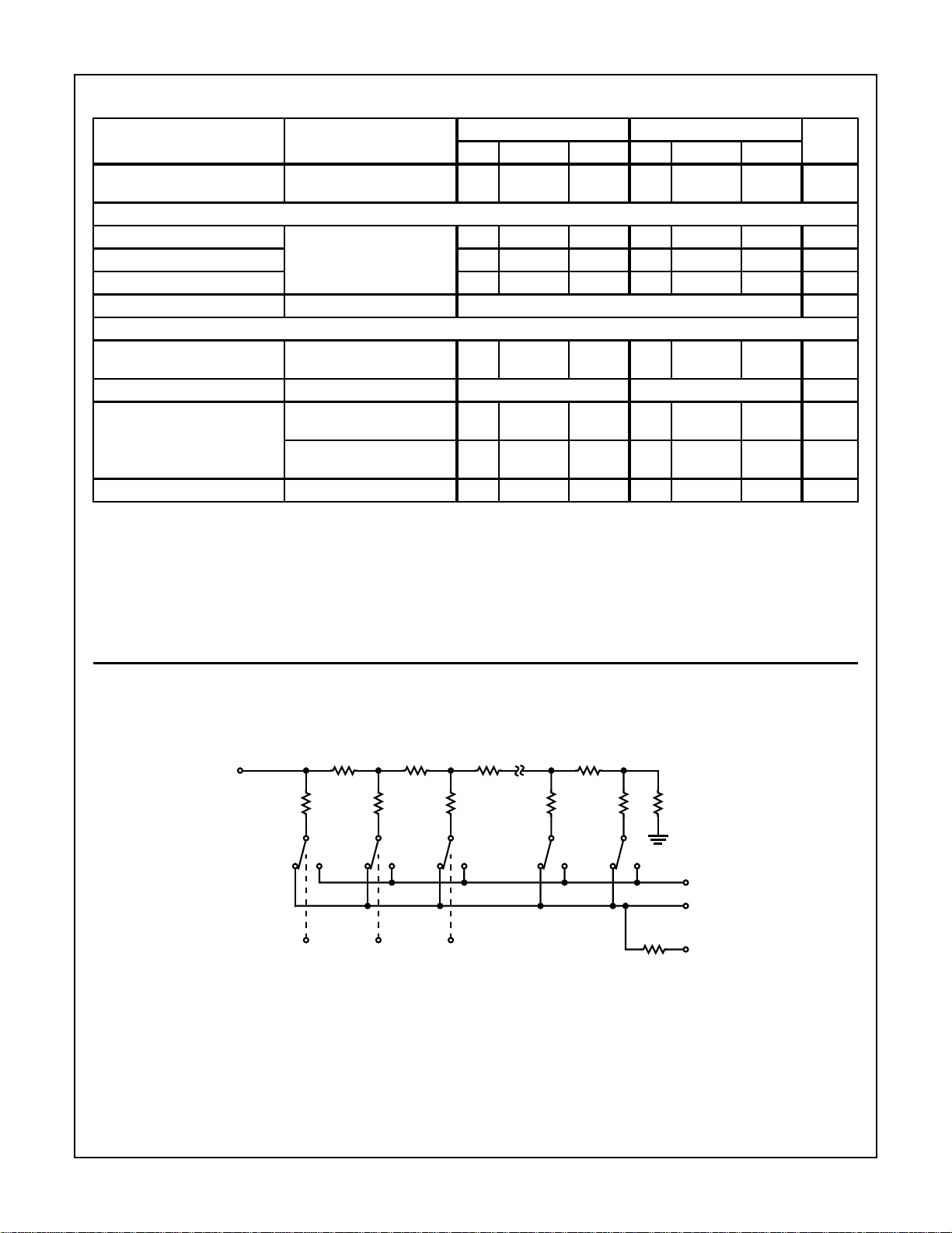
Functional Diagram
V
REF
SPDT NMOS
SWITCHES
NOTES:
Switches shown for Digital Inputs “High”.
Resistor values are typical.
10kΩ 10kΩ 10kΩ 10kΩ
BIT 3BIT 2MSB
10kΩ
20kΩ
GND
I
OUT2
I
OUT1
R
FEEDBACK
20kΩ20kΩ20kΩ20kΩ20kΩ
10-9
 Loading...