

查询ACS04K/SAMPLE-03供应商
®
AD7520, AD7521
Data Sheet August 2002
10-Bit, 12-Bit, Multiplying D/A Converters
The AD7520 and AD7521 are monolithic, high accuracy, low
cost 10-bit and 12-bit resolution, multiplying digital-to-analog
converters (DAC). Intersil’s thin-film on CMOS processing
gives up to 10-bit accuracy with TTL/CMOS compatible
operation. Digital inputs are fully protected against static
discharge by diodes to ground and positive supply.
Typical applications include digital/analog interfacing,
multiplication and division, programmable power supplies,
CRT character generation, digitally controlled gain circuits,
integrators and attenuators, etc.
Ordering Information
TEMP.
PART
NUMBER
LINEARITY
(INL, DNL)
AD7520JN 0.2% (8-Bit) 0 to 70 16 Ld PDIP E16.3
AD7521LN 0.05% (10-
Bit)
RANGE
o
(
C) PACKAGE
PKG.
0 to 70 18 Ld PDIP E18.3
NO.
FN3104.4
Features
• AD7520, 10-Bit Resolution; 8-Bit Linearity
• AD7521, 12-Bit Resolution; 10-Bit Linearity
• Low Power Dissipation (Max). . . . . . . . . . . . . . . . . 20mW
o
• Low Nonlinearity Tempco at 2ppm of FSR/
• Current Settling Time to 0.05% of FSR . . . . . . . . . . 1.0µs
• Supply Voltage Range . . . . . . . . . . . . . . . . . ±5V to +15V
• TTL/CMOS Compatible
• Full Input Static Protection
C
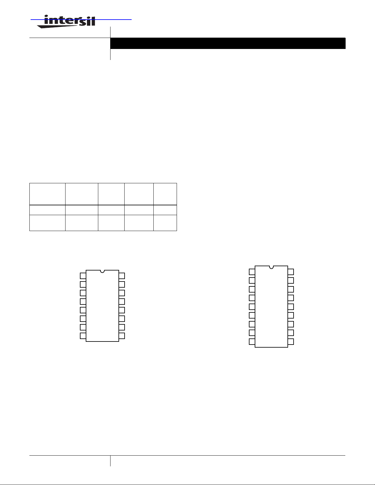
Pinouts
I
OUT1
I
OUT2
GND
BIT 1 (MSB)
BIT 2
BIT 3
BIT 4
BIT 5
AD7520 (PDIP)
TOP VIEW
1
2
3
4
5
6
7
8
R
16
FEEDBACK
V
15
REF
14
V+
BIT 10 (LSB)
13
BIT 9
12
BIT 8
11
BIT 7
10
BIT 6
9
I
OUT1
I
OUT2
GND
BIT 1 (MSB)
BIT 2
BIT 3
BIT 4
BIT 5
BIT 6
AD7521 (PDIP)
TOP VIEW
1
2
3
4
5
6
7
8
9
18
R
FEEDBACK
V
17
REF
16
V+
15
BIT 12 (LSB)
14
BIT 11
13
BIT 10
12
BIT 9
11
BIT 8
BIT 7
10
1
CAUTION: These devices are sensitive to electrostatic discharge; follow proper IC Handling Procedures.
1-888-INTERSIL or 321-724-7143
| Intersil (and design) is a registered trademark of Intersil Americas Inc.
Copyright © Intersil Americas Inc. 2002. All Rights Reserved
AD7520, AD7521
Absolute Maximum Ratings Thermal Information
Supply Voltage (V+ to GND) . . . . . . . . . . . . . . . . . . . . . . . . . . .+17V
V
. . . . . . . . . . . . . . . . . . . . . . . . . . . . . . . . . . . . . . . . . . . . ±25V
REF
Digital Input Voltage Range . . . . . . . . . . . . . . . . . . . . . . . V+ to GND
Output Voltage Compliance . . . . . . . . . . . . . . . . . . . . . -100mV to V+
Operating Conditions
Temperature Ranges
JN, LN Versions . . . . . . . . . . . . . . . . . . . . . . . . . . . . . 0
CAUTION: Stresses above those listed in “Absolute Maximum Ratings” may cause permanent damage to the device. This is a stress only rating and operation of the
device at these or any other conditions above those indicated in the operational sections of this specification is not implied.
The digital control inputs are zener protected; however, permanent damage may occur on unconnected units under high energy electrostatic fields. Keep unused units in
conductive foam at all times.
Do not apply voltages higher than V
or less than GND potential on any terminal except V
DD
o
C to 70oC
Thermal Resistance (Typical, Note 1) θ
16 Ld PDIP Package 90 N/A
18 Ld PDIP Package 80 N/A
Maximum Junction Temperature (Plastic Packages) . . . . . . . 150
Maximum Storage Temperature Range. . . . . . . . . . -65
Maximum Lead Temperature (Soldering 10s) . . . . . . . . . . . . .300
REF
and R
FEEDBACK
.
1. θJA is measured with the component mounted on a low effective thermal conductivity test board in free air. See Tech Brief TB379 for details.
(oC/W) θJC (oC/W)
JA
o
C to 150oC
o
o
C
C
Electrical Specifications V+ = +15V, V
= +10V, TA = 25oC Unless Otherwise Specified
REF
AD7520 AD7521
PARAMETER TEST CONDITIONS
UNITSMIN TYP MAX MIN TYP MAX
SYSTEM PERFORMANCE (Note 2)
Resolution 10 10 10 12 12 12 Bits
Nonlinearity J (Note 3) (Figure 2)
-10V ≤ V
L -10V ≤ V
REF
REF
≤ +10V
≤ +10V
(Figure 2)
Nonlinearity Tempco -10V ≤ V
(Notes 3, 4)
REF
≤ +10V
--±0.2
(8-Bit)
--±0.05
(10-Bit)
-- ±2- - ±2 ppm of
-- -% of
FSR
--±0.05
(10-Bit)
% of
FSR
FSR/
Gain Error - ±0.3 - - ±0.3 - % of
FSR
Gain Error Tempco - - ±10 - - ±10 ppm of
FSR/
Output Leakage Current
(Either Output)
Over the Specified
Temperature Range
--±200 - - ±200 nA
DYNAMIC CHARACTERISTICS
Output Current Settling Time To 0.05% of FSR (All Digital
-1.0 - -1.0 - µs
Inputs Low To High And High
To Low) (Note 4) (Figure 7)
Feedthrough Error V
= 20V
REF
All Digital Inputs Low (Note 4)
P-P
, 100kHz
- - 10 - - 10 mV
P-P
(Figure 6)
REFERENCE INPUT
Input Resistance All Digital Inputs High
I
at Ground
OUT1
5 10 20 5 10 20 kΩ
ANALOG OUTPUT
Output Capacitance I
All Digital Inputs High
OUT1
(Note 4) (Figure 5)
I
OUT2
All Digital Inputs Low
I
OUT1
(Note 4) (Figure 5)
I
OUT2
Output Noise Both Outputs
(Note 4) (Figure 4)
- 200 - - 200 - pF
-75--75-pF
-75--75-pF
- 200 - - 200 - pF
- Equivalent
to 10kΩ
- - Equivalent
to 10kΩ
- Johnson
Noise
DIGITAL INPUTS
Low State Threshold, V
High State Threshold, V
Input Current, I
, I
IL
IH
IL
IH
Over the Specified
Temperature Range
V
= 0V or +15V
IN
-- 0.8-- 0.8V
2.4 - - 2.4 - - V
-- ±1- - ±1 µA
Input Coding See Tables 1 and 2 Binary/Offset Binary
o
C
o
C
2
AD7520, AD7521
Electrical Specifications V+ = +15V, V
= +10V, TA = 25oC Unless Otherwise Specified (Continued)
REF
AD7520 AD7521
PARAMETER TEST CONDITIONS
UNITSMIN TYP MAX MIN TYP MAX
POWER SUPPLY CHARACTERISTICS
Power Supply Rejection V+ = 14.5V to 15.5V
(Note 3) (Figure 3)
- ±0.005 - - ±0.005 - %
FSR/%
∆V+
Power Supply Voltage Range +5 to +15 +5 to +15 V
I+ All Digital Inputs at 0V or V+
- ±1--±1-µA
Excluding Ladder Network
All Digital Inputs High or Low
-- 2-- 2mA
Excluding Ladder Network
Total Power Dissipation Including the Ladder Network - 20 - - 20 - mW
NOTES:
2. Full Scale Range (FSR) is 10V for Unipolar and ±10V for Bipolar modes.
3. Using internal feedback resistor R
FEEDBACK
.
4. Guaranteed by design, or characterization and not production tested.
5. Accuracy not guaranteed unless outputs at GND potential.
6. Accuracy is tested and guaranteed at V+ = 15V only.
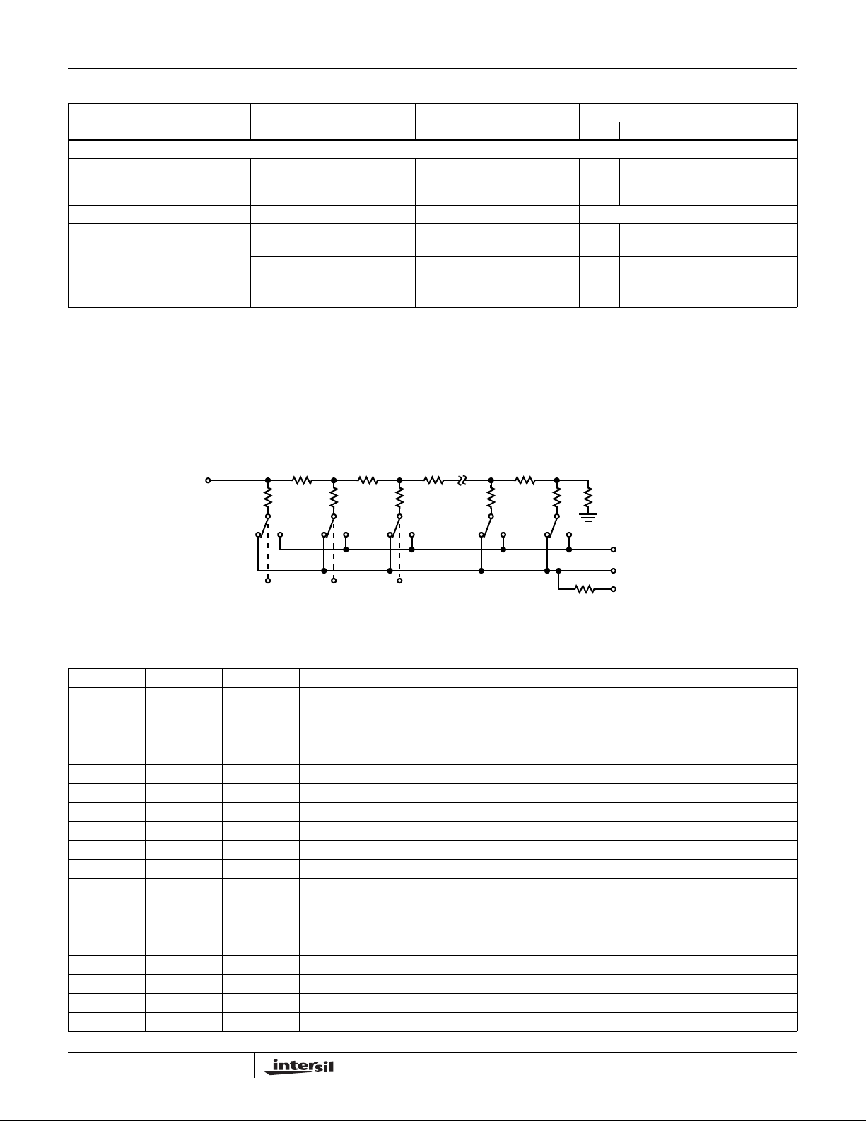
Functional Diagram
V
REF
10kΩ 10kΩ 10kΩ 10kΩ
20kΩ20kΩ20kΩ20kΩ20kΩ
20kΩ
GND
SPDT NMOS
SWITCHES
NOTES:
BIT 3BIT 2MSB
Switches shown for Digital Inputs “High”.
Resistor values are typical.
Pin Descriptions
AD7520 AD7521 PIN NAME DESCRIPTION
11I
22I
OUT1
OUT2
3 3 GND Digital Ground. Ground potential for digital side of D/A.
4 4 Bits 1(MSB) Most Significant Digital Data Bit.
5 5 Bit 2 Digital Bit 2.
6 6 Bit 3 Digital Bit 3.
7 7 Bit 4 Digital Bit 4.
8 8 Bit 5 Digital Bit 5.
9 9 Bit 6 Digital Bit 6.
10 10 Bit 7 Digital Bit 7.
11 11 Bit 8 Digital Bit 8.
12 12 Bit 9 Digital Bit 9.
13 13 Bit 10 Digital Bit 10 (AD7521). Least Significant Digital Data Bit (AD7520).
- 14 Bit 11 Digital Bit 11 (AD7521).
- 15 Bit 12 Least Significant Digital Data Bit (AD7521).
14 16 V+ Power Supply +5V to +15V.
15 17 V
16 18 R
REF
FEEDBACK
Current Out summing junction of the R2R ladder network.
Current Out virtual ground, return path for the R2R ladder network.
Voltage Reference Input to set the output range. Supplies the R2R resistor ladder.
Feedback resistor used for the current to voltage conversion when using an external Op Amp.
10kΩ
I
OUT2
I
OUT1
R
FEEDBACK
3

AD7520, AD7521
Definition of Terms
Nonlinearity: Error contributed by deviation of the DAC
transfer function from a “best straight line” through the actual
plot of transfer function. Normally expressed as a
percentage of full scale range or in (sub)multiples of 1 LSB.
Resolution: It is addressing the smallest distinct analog
output change that a D/A converter can produce. It is
commonly expressed as the number of converter bits. A
converter with resolution of N bits can resolve output changes
-N
of 2
of the full-scale range, e.g., 2-N V
for a unipolar
REF
conversion. Resolution by no means implies linearity.
Settling Time: Time required for the output of a DAC to
settle to within specified error band around its final value
1
(e.g.,
/2 LSB) for a given digital input change, i.e., all digital
inputs LOW to HIGH and HIGH to LOW.
Gain Error: The difference between actual and ideal analog
output values at full scale range, i.e., all digital inputs at
HIGH state. It is expressed as a percentage of full scale
range or in (sub)multiples of 1 LSB.
Feedthrough Error: Error caused by capacitive coupling
from V
Output Capacitance: Capacitance from I
REF
to I
with all digital inputs LOW.
OUT1
OUT1
and I
OUT2
terminals to ground.
Output Leakage Current: Current which appears on I
terminal when all digital inputs are LOW or on I
OUT2
OUT1
terminal
when all digital inputs are HIGH.
Detailed Description
The AD7520 and AD7521 are monolithic, multiplying D/A
converters. A highly stable thin film R-2R resistor ladder
network and NMOS SPDT switches form the basis of the
converter circuit, CMOS level shifters permit low power
TTL/CMOS compatible operation. An external voltage or
current reference and an operational amplifier are all that is
required for most voltage output applications.
A simplified equivalent circuit of the DAC is shown in the
Functional Diagram. The NMOS SPDT switches steer the
ladder leg currents between I
OUT1
and I
buses which
OUT2
must be held either at ground potential. This configuration
maintains a constant current in each ladder leg independent
of the input code.
Converter errors are further reduced by using separate
metal interconnections between the major bits and the
outputs. Use of high threshold switches reduce offset
(leakage) errors to a negligible level.
The level shifter circuits are comprised of three inverters with
positive feedback from the output of the second to the first, see
Figure 1. This configuration results in TTL/CMOS compatible
operation over the full military temperature range. With the
ladder SPDT switches driven by the level shifter, each switch is
binarily weighted for an ON resistance proportional to the
respective ladder leg current. This assures a constant voltage
drop across each switch, creating equipotential terminations for
the 2R ladder resistors and highly accurate leg currents.
CMOS INPUT
V+
DTL/TTL/
13
4
6
5
72
FIGURE 1. CMOS LEVEL SHIFTER AND SWITCH
TO LADDER
89
I
OUT2IOUT1
Test Circuits The following test circuits apply for the AD7520. Similar circuits are used for the AD7521.
V
10-BIT
BINARY
COUNTER
CLOCK
BIT 1
(MSB)
BIT 10
(LSB)
BIT 1
(MSB)
BIT 10
BIT 11
BIT 12
REF
+15V
R
15
4
5
AD7520
13
32
GND
V
REF
12-BIT
REFERENCE
16
DAC
I
1
I
OUT2
FEEDBACK
OUT1
10kΩ 0.01%
-
HA2600
+
10kΩ
0.01%
-
HA2600
+
1MΩ
LINEARITY
ERROR
x 100
+10V
V
REF
BIT 1
(MSB)
BIT 10
(LSB)
GND
+15V
15
14
4
16
5
AD7520
13
32
R
I
OUT1
1
I
OUT2
UNGROUNDED
SINE WAVE
GENERATOR
40Hz 1V
5K 0.01%
FEEDBACK
FIGURE 2. NONLINEARITY FIGURE 3. POWER SUPPLY REJECTION
4
P-P
5kΩ 0.01%
-
HA2600
+
500kΩ
-
HA2600
+
V
ERROR
x 100

AD7520, AD7521
Test Circuits The following test circuits apply for the AD7520. Similar circuits are used for the AD7521. (Continued)
+11V (ADJUST FOR V
1K
15µF
100kHz SINE WAVE
= 20V
V
REF
BIT 1 (MSB)
BIT 10 (LSB)
15
4
5
AD7520
13
3
P-P
= 0V)
OUT
+15V
14
2
1
I
OUT2
I
OUT1
50kΩ
100Ω
1kΩ
0.1µF
10kΩ
-
101ALN
+
-50V
V
OUT
f = 1kHz
BW = 1Hz
QUAN
TECH
MODEL 134D
WAVE
ANALYZER
+15V
BIT 1 (MSB)
BIT 10 (LSB)
+15VNC
15
14
4
5
AD7520
1332
16
1
FIGURE 4. NOISE FIGURE 5. OUTPUT CAPACITANCE
+15V
15
4
5
AD7520
13
3
14
16
GND
V
REF
+10V
BIT 1 (MSB)
I
OUT1
3
2
-
HA2600
+
6
V
OUT
1
I
OUT2
2
+5V
0V
DIGITAL
INPUT
BIT 10 (LSB)
EXTRAPOLATE
+15V
15
14
4
5
AD7520
1
1332
I
GND
+100mV
OUT2
NC
1kΩ
100mV
SCOPE
1MHz
5t: 1% SETTLING (1mV)
8t: 0.03% SETTLING
t = RISE TIME
100Ω
P-P
SCOPE
FIGURE 6. FEEDTHROUGH ERROR FIGURE 7. OUTPUT CURRENT SETTLING TIME
Applications
Unipolar Binary Operation
The circuit configuration for operating the AD7520 in
unipolar mode is shown in Figure 8. Similar circuits can be
used for AD7521. With positive and negative V
the circuit is capable of 2-Quadrant multiplication. The Digital
Input Code/Analog Output Value table for unipolar mode is
given in Table 1.
15
4
5
AD7520
13
3
+15V
14
16
GND
1
2
R
FEEDBACK
I
OUT1
I
OUT2
V
REF
BIT 1 (MSB)
DIGITAL
INPUT
BIT 10 (LSB)
FIGURE 8. UNIPOLAR BINARY OPERATION (2-QUADRANT
MULTIPLICATION)
values
REF
-
V
6
+
OUT
TABLE 1. CODE TABLE - UNlPOLAR BINARY OPERATION
DIGITAL INPUT ANALOG OUTPUT
1111111111 -V
1000000001 -V
1000000000 -V
0111111111 -V
0000000001 -V
REF
REF
REF
REF
REF
(1-2-N)
/2
(1/2-2-N)
(2-N)
(1/2 + 2-N)
0000000000 0
NOTES:
-N
V
1. LSB = 2
REF
.
2. N = 8 for 7520
N = 10 for 7521.
Zero Offset Adjustment
1. Connect all digital inputs to GND.
2. Adjust the offset zero adjust trimpot of the output
operational amplifier for 0V at V
OUT
.
Gain Adjustment
1. Connect all digital inputs to V+.
2. Monitor V
AD7520 and N = 10 for AD7521).
OUT
for a -V
(1-2-N) reading. (N = 8 for
REF
5

AD7520, AD7521
3. To decrease V
between the reference voltage and the V
4. To increase V
in the I
OUT1
, connect a series resistor (0 to 250Ω)
OUT
REF
, connect a series resistor (0 to 250Ω)
OUT
amplifier feedback loop.
terminal.
Bipolar (Offset Binary) Operation
The circuit configuration for operating the AD7520 in the
bipolar mode is given in Figure 9. Similar circuits can be
used for AD7521. Using offset binary digital input codes
and positive and negative reference voltage values,
4-Quadrant multiplication can be realized. The “Digital
Input Code/Analog Output Value” table for bipolar mode is
given in Table 2.
V
REF
BIT 1
(MSB)
INPUT
DIGITAL
BIT 10
(LSB)
FIGURE 9. BIPOLAR OPERATION (4-QUADRANT
TABLE 2. BlPOLAR (OFFSET BINARY) CODE TABLE
DIGITAL INPUT ANALOG OUTPUT
NOTES:
1. LSB = 2
+15V
15
14
R
V
16
1
2
REF
FEEDBACK
I
OUT1
I
OUT2
.
-
6
+
R1 10K
0.01%
4
5
AD7520
13
3
MULTIPLICATION)
1111111111 -V
1000000001 -V
1000000000 0
0111111111 V
0000000001 V
0000000000 V
-(N-1)
2. N = 8 for 7520
R3
10MΩ
R2 10K
0.01%
-(N-1)
(1-2
REF
-(N-1)
(2
REF
-(N-1)
(2
REF
-(N-1)
(1-2
REF
REF
N = 10 for 7521.
-
6
+
)
)
)
)
A “Logic 1” input at any digital input forces the corresponding
ladder switch to steer the bit current to IOUT1 bus. A “Logic 0”
input forces the bit current to IOUT2 bus. For any code the
IOUT1 and IOUT2 bus currents are complements of one
another. The current amplifier at IOUT2 changes the polarity
of IOUT2 current and the transconductance amplifier at
IOUT1 output sums the two currents. This configuration
doubles the output range. The difference current resulting
at zero offset binary code, (MSB = “Logic 1”, all other
bits = “Logic 0”), is corrected by using an external resistor,
(10MW), from VREF to IOUT2 .
Offset Adjustment
1. Adjust V
2. Connect all digital inputs to “Logic 1”.
3. Adjust I
I
OUT2
4. Connect MSB (Bit 1) to “Logic 1” and all other bits to
“Logic 0”.
OUT
V
5. Adjust I
at V
OUT
to approximately +10V.
REF
amplifier offset adjust trimpot for 0V ±1mV at
OUT2
amplifier output.
amplifier offset adjust trimpot for 0V ±1mV
OUT1
.
Gain Adjustment
1. Connect all digital inputs to V+.
2. Monitor V
OUT
for a -V
REF
AD7520, and N = 10 for AD7521.).
3. To increase V
between V
4. To decrease V
, connect a series resistor of up to 250Ω
OUT
and R
OUT
, connect a series resister of up to 250Ω
OUT
between the reference voltage and the V
-(N-1)
(1-2
FEEDBACK
volts reading. (N = 8 for
.
terminal.
REF
6

Die Characteristics
AD7520, AD7521
DIE DIMENSIONS:
101 mils x 103 mils (2565µm x 2616µm)
METALLIZATION:
Type: Pure Aluminum
Thickness: 10 ±1k
Å
Metallization Mask Layout
PIN 7
BIT 4
PIN 8
BIT 5
PIN 6
BIT 3
AD7520
PIN 5
BIT 2
PAS SIVATIO N:
Type: PSG/Nitride
PSG: 7 ±1.4kÅ
Nitride: 8 ±1.2kÅ
PROCESS:
CMOS Metal Gate
PIN 4
BIT 1
(MSB)
PIN 3
GND
PIN 2
I
OUT
PIN 1
I
OUT
2
1
PIN 9
BIT 6
PIN 10
BIT 7
PIN 11
BIT 8
BIT 9
PIN 13
BIT 10
(LSB)
PIN 16
R
FEEDBACK
PIN 15
V
REF
PIN 14
V+
NCNCPIN 12
7

Die Characteristics
AD7520, AD7521
DIE DIMENSIONS:
101 mils x 103 mils (2565µm x 2616µm)
METALLIZATION:
Type: Pure Aluminum
Thickness: 10 ±1k
Å
Metallization Mask Layout
PIN 7
BIT 4
PIN 8
BIT 5
PIN 6
BIT 3
AD7521
PIN 5
BIT 2
PAS SIVATIO N:
Type: PSG/Nitride
PSG: 7 ±1.4kÅ
Nitride: 8 ±1.2kÅ
PROCESS:
CMOS Metal Gate
PIN 4
BIT 1
(MSB)
PIN 3
GND
PIN 2
I
OUT
PIN 1
I
OUT
2
1
PIN 9
BIT 6
PIN 10
BIT 7
PIN 11
BIT 8
PIN 12
BIT 9
PIN 13
BIT 10
PIN 14
BIT 11
PIN 15
BIT 12
(LSB)
PIN 18
R
FEEDBACK
PIN 17
V
REF
PIN 16
V+
8

Dual-In-Line Plastic Packages (PDIP)
AD7520, AD7521
N
D1
-C-
E1
-B-
A1
A2
E
A
L
e
C
C
L
e
A
C
e
B
INDEX
AREA
BASE
PLANE
SEATING
PLANE
D1
B1
12 3 N/2
-AD
e
B
0.010 (0.25) C AM BS
NOTES:
1. Controlling Dimensions: INCH. In case of conflict between English and
Metric dimensions, the inch dimensions control.
2. Dimensioning and tolerancing per ANSI Y14.5M-1982.
3. Symbols are defined in the “MO Series Symbol List” in Section 2.2 of
Publication No. 95.
4. Dimensions A, A1 and L are measured with the package seated in JEDEC seating plane gauge GS-3.
5. D, D1, and E1 dimensions do not include mold flash or protrusions.
Mold flash or protrusions shall not exceed 0.010 inch (0.25mm).
6. E and are measured with the leads constrained to be perpendic-
7. e
e
A
ular to datum .
and eC are measured at the lead tips with the leads unconstrained.
B
e
must be zero or greater.
C
-C-
8. B1 maximum dimensions do not include dambar protrusions. Dambar
protrusions shall not exceed 0.010 inch (0.25mm).
9. N is the maximum number of terminal positions.
10. Corner leads (1, N, N/2 and N/2 + 1) for E8.3, E16.3, E18.3, E28.3,
E42.6 will have a B1 dimension of 0.030 - 0.045 inch (0.76 - 1.14mm).
E16.3 (JEDEC MS-001-BB ISSUE D)
16 LEAD DUAL-IN-LINE PLASTIC PACKAGE
INCHES MILLIMETERS
SYMBOL
A - 0.210 - 5.33 4
A1 0.015 - 0.39 - 4
A2 0.115 0.195 2.93 4.95 -
B 0.014 0.022 0.356 0.558 -
B1 0.045 0.070 1.15 1.77 8, 10
C 0.008 0.014 0.204 0.355 -
D 0.735 0.775 18.66 19.68 5
D1 0.005 - 0.13 - 5
E 0.300 0.325 7.62 8.25 6
E1 0.240 0.280 6.10 7.11 5
e 0.100 BSC 2.54 BSC -
e
A
e
B
0.300 BSC 7.62 BSC 6
- 0.430 - 10.92 7
L 0.115 0.150 2.93 3.81 4
N16 169
NOTESMIN MAX MIN MAX
Rev. 0 12/93
9

Dual-In-Line Plastic Packages (PDIP)
AD7520, AD7521
N
D1
-C-
E1
-B-
A1
A2
E
A
L
e
C
C
L
e
A
C
e
B
INDEX
AREA
BASE
PLANE
SEATING
PLANE
D1
B1
12 3 N/2
-AD
e
B
0.010 (0.25) C AM BS
NOTES:
1. Controlling Dimensions: INCH. In case of conflict between English and
Metric dimensions, the inch dimensions control.
2. Dimensioning and tolerancing per ANSI Y14.5M-1982.
3. Symbols are defined in the “MO Series Symbol List” in Section 2.2 of
Publication No. 95.
4. Dimensions A, A1 and L are measured with the package seated in
JEDEC seating plane gauge GS-3.
5. D, D1, and E1 dimensions do not include mold flash or protrusions.
Mold flash or protrusions shall not exceed 0.010 inch (0.25mm).
6. E and are measured with the leads constrained to be perpendic-
7. e
e
A
ular to datum .
and eC are measured at the lead tips with the leads unconstrained.
B
e
must be zero or greater.
C
-C-
8. B1 maximum dimensions do not include dambar protrusions. Dambar
protrusions shall not exceed 0.010 inch (0.25mm).
9. N is the maximum number of terminal positions.
10. Corner leads (1, N, N/2 and N/2 + 1) for E8.3, E16.3, E18.3, E28.3,
E42.6 will have a B1 dimension of 0.030 - 0.045 inch (0.76 - 1.14mm).
E18.3 (JEDEC MS-001-BC ISSUE D)
18 LEAD DUAL-IN-LINE PLASTIC PACKAGE
INCHES MILLIMETERS
SYMBOL
A - 0.210 - 5.33 4
A1 0.015 - 0.39 - 4
A2 0.115 0.195 2.93 4.95 -
B 0.014 0.022 0.356 0.558 -
B1 0.045 0.070 1.15 1.77 8, 10
C 0.008 0.014 0.204 0.355 -
D 0.845 0.880 21.47 22.35 5
D1 0.005 - 0.13 - 5
E 0.300 0.325 7.62 8.25 6
E1 0.240 0.280 6.10 7.11 5
e 0.100 BSC 2.54 BSC -
e
A
e
B
0.300 BSC 7.62 BSC 6
- 0.430 - 10.92 7
L 0.115 0.150 2.93 3.81 4
N18 189
NOTESMIN MAX MIN MAX
Rev. 0 12/93
All Intersil products are manufactured, assembled and tested utilizing ISO9000 quality systems.
Intersil Corporation’s quality certifications can be viewed at website www.intersil.com/design/quality
Intersil products are sold by description only. Intersil Corporation reserves the right to make changes in circuit design and/or specifications at any time without notice.
Accordingly, the reader is cautioned to verify that data sheets are current before placing orders. Information furnished by Intersil is believed to be accurate and reliable. However, no responsibility is assumed by Intersil or its subsidiaries for its use; nor for any infringements of patents or other rights of third parties which may result from its use. No
license is granted by implication or otherwise under any patent or patent rights of Intersil or its subsidiaries.
For information regarding Intersil Corporation and its products, see web site www.intersil.com
10
 Loading...