Intersil Corporation ACTS373MS Datasheet

April 1995
ACTS373MS
Radiation Hardened
Octal Transparent Latch, Three-State
Features
• 1.25 Micron Radiation Hardened SOS CMOS
• Total Dose 300K RAD (Si)
• Single Event Upset (SEU) Immunity
<1 x 10
• SEU LET Threshold >80 MEV-cm
• Dose Rate Upset >10
-10
Errors/Bit-Day (Typ)
11
RAD (Si)/s, 20ns Pulse
2
/mg
• Latch-Up Free Under Any Conditions
o
• Military Temperature Range: -55
C to +125oC
• Significant Power Reduction Compared to ALSTTL Logic
• DC Operating Voltage Range: 4.5V to 5.5V
• Input Logic Levels
- VIL = 0.8V Max
- VIH = VCC/2V Min
• Input Current ≤1µA at VOL, VOH
Description
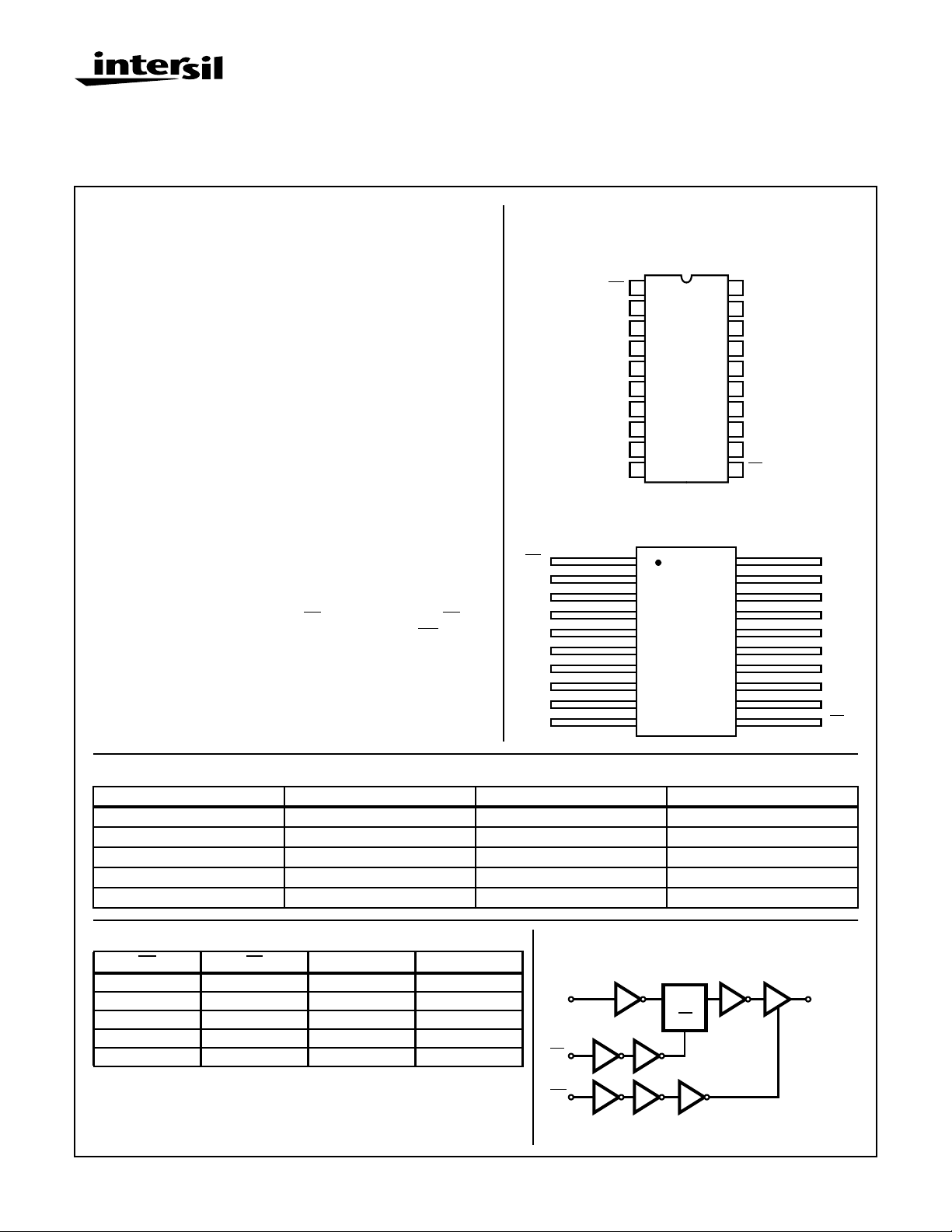
The Intersil ACTS373MS is a radiation hardened octal transparent latch with three-state outputs. The outputs are transparent to
the inputs when the latch enable (
low, the data is latched. When the Output Enable (
the outputs are in the high impedance state. The latch operation
is independent of the state of the output enable.
The ACTS373MS utilizes advanced CMOS/SOS technology to
achieve high-speed operation. This device is a member of the
radiation hardened, high-speed, CMOS/SOS Logic Family.
LE) is high. When the LE goes
OE) is high,
Pinouts
20 LEAD CERAMIC DUAL-IN-LINE
MIL-STD-1835 DESIGNATOR, CDIP2-T20, LEAD FINISH C
TOP VIEW
1
OE
Q0
2
D0
3
D1
4
Q1
5
Q2
6
D2
7
8
D3
9
Q3
GND
10
20 LEAD CERAMIC FLATPACK
MIL-STD-1835 DESIGNATOR, CDFP4-F20, LEAD FINISH C
TOP VIEW
OE
Q0
D0
D1
Q1
Q2
D2
D3
Q3
GND
120
2
3
4
5
6
7
8
9
10
VCC
20
Q7
19
D7
18
D6
17
Q6
16
Q5
15
D5
14
D4
13
12
Q4
11
LE
VCC
19
18
17
16
15
14
13
12
11
Q7
D7
D6
Q6
Q5
D5
D4
Q4
LE
Ordering Information
PART NUMBER TEMPERATURE RANGE SCREENING LEVEL PACKAGE
ACTS373DMSR -55oC to +125oC Intersil Class S Equivalent 20 Lead SBDIP
ACTS373KMSR -55oC to +125oC Intersil Class S Equivalent 20 Lead Ceramic Flatpack
ACTS373D/Sample +25oC Sample 20 Lead SBDIP
ACTS373K/Sample +25oC Sample 20 Lead Ceramic Flatpack
ACTS373HMSR +25oC Die Die
Truth Table
OE LE D Q
LHHH
LHLL
LLIL
LLhH
HXXZ
NOTE:
L = Low Voltage Level
H = High Voltage Level
I = Low voltage level one set-up time prior to the high to low latch enable transition
h = High voltage level one set-up time prior to the high to low latch enable transition
CAUTION: These devices are sensitive to electrostatic discharge; follow proper IC Handling Procedures.
1-888-INTERSIL or 321-724-7143 | Copyright © Intersil Corporation 1999
X = Don’t Care
Z = High Impedance State
1
Functional Diagram
1 OF 8
(3, 4, 7, 8, 13,
14, 17, 18)
D
COMMON
CONTROLS
LE
(11)
OE
(1)
LATCH
DQ
LE
Spec Number 518800
File Number 4000
OE
Q
(2, 5, 6, 9, 12,
15, 16, 19)

Specifications ACTS373MS
Absolute Maximum Ratings Reliability Information
Supply Voltage . . . . . . . . . . . . . . . . . . . . . . . . . . . . . .-0.5V to +6.0V
Input Voltage Range, All Inputs . . . . . . . . . . . . .-0.5V to VCC +0.5V
DC Input Current, Any One Input . . . . . . . . . . . . . . . . . . . . . . . .±10mA
DC Drain Current, Any One Output. . . . . . . . . . . . . . . . . . . . . . .±50mA
Storage Temperature Range (TSTG). . . . . . . . . . . -65oC to +150oC
Lead Temperature (Soldering 10s). . . . . . . . . . . . . . . . . . . . +265
Junction Temperature (TJ) . . . . . . . . . . . . . . . . . . . . . . . . . . +175
ESD Classification . . . . . . . . . . . . . . . . . . . . . . . . . . . . . . . . Class 1
(All Voltages Reference to VSS)
CAUTION: As with all semiconductors, stress listed under “Absolute Maximum Ratings” may be applied to devices (one at a time) without resulting in permanent
damage. This is a stress rating only. Exposure to absolute maximum rating conditions for extended periods may affect device reliability. The conditions listed
under “Electrical Performance Characteristics” are the only conditions recommended for satisfactory device operation.
Operating Conditions
Supply Voltage (VCC). . . . . . . . . . . . . . . . . . . . . . . . +4.5V to +5.5V
Input Rise and Fall Times at VCC = 4.5V (TR, TF) . . . . 10ns/V Max
Operating Temperature Range (T
) . . . . . . . . . . . . -55oC to +125oC
A
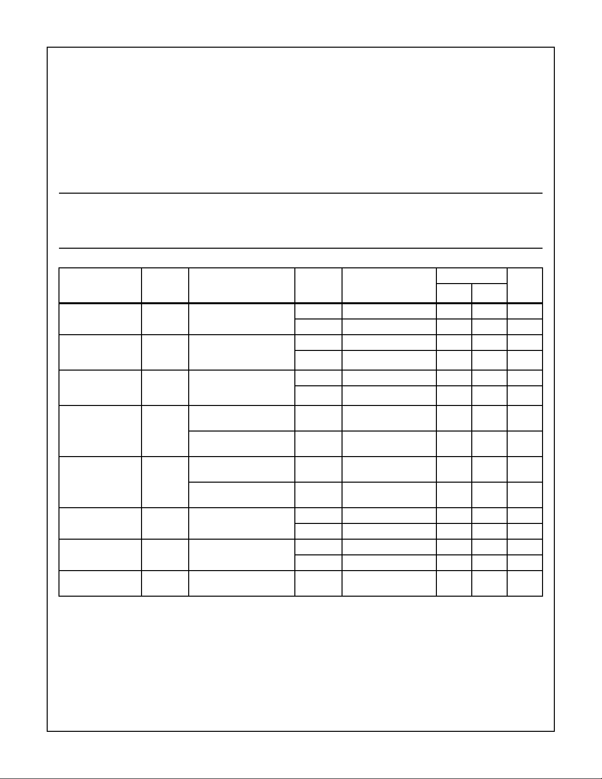
TABLE 1. DC ELECTRICAL PERFORMANCE CHARACTERISTICS
Thermal Impedance θ
DIP. . . . . . . . . . . . . . . . . . . . . . . . . . . . . . 72oC/W 24oC/W
Flatpack. . . . . . . . . . . . . . . . . . . . . . . . . . 107
Maximum Package Power Dissipation at +125
DIP. . . . . . . . . . . . . . . . . . . . . . . . . . . . . . . . . . . . . . . . . . . . . 0.7W
o
C
Flatpack. . . . . . . . . . . . . . . . . . . . . . . . . . . . . . . . . . . . . . . . . 0.5W
o
C
Maximum Device Power Dissipation. . . . . . . . . . . . . . . . . . .(TBD)W
JA
o
C/W 28oC/W
o
C
Gate Count . . . . . . . . . . . . . . . . . . . . . . . . . . . . . . . . . . . .121 Gates
Input High Voltage (VIH). . . . . . . . . . . . . . . . . . . . . VCC to VCC/2V
Input Low Voltage (VIL). . . . . . . . . . . . . . . . . . . . . . . . . . .0V to 0.8V
θ
JC
GROUP
(NOTE 1)
PARAMETER SYMBOL
CONDITIONS
Supply Current ICC VCC = 5.5V,
VIN = VCC or GND
Output Current
(Source)
IOH VCC = VIH = 4.5V,
VOUT = VCC -0.4V,
VIL = 0V, (Note 2)
Output Current
(Sink)
IOL VCC = VIH = 4.5V,
VOUT = 0.4V, VIL = 0V,
(Note 2)
Output Voltage High VOH VCC = 5.5V, VIH = 2.75V
A SUB-
GROUPS TEMPERATURE
1 +25
o
C-20µA
2, 3 +125oC, -55oC - 400 µA
1 +25oC -12 - mA
2, 3 +125oC, -55oC-8-mA
1 +25oC12-mA
2, 3 +125oC, -55oC8-mA
1, 2, 3 +25oC, +125oC, -55oC VCC -
VIL = 0.8V, IOH = -50µA
VCC = 4.5V, VIH = 2.25V,
1, 2, 3 +25oC, +125oC, -55oC VCC -
VIL = 0.8V, IOH = -50µA
Output Voltage Low VOL VCC = 5.5V, VIH = 2.75V
1, 2, 3 +25oC, +125oC, -55oC - 0.1 V
VIL = 0.8V, IOH = 50µA
VCC = 4.5V, VIH = 2.25V,
1, 2, 3 +25oC, +125oC, -55oC - 0.1 V
VIL = 0.8V, IOH = 50µA
Input Leakage
Current
Three-State Output
Leakage Current
Noise Immunity
Functional Test
IIN VCC = 5.5V,
VIN = VCC or GND
IOZ VCC = 5.5V,
Force Voltage = 0V or VCC
FN VCC = 4.5V, VIH = 2.25V,
VIL = 0.8V, (Note 3)
1 +25oC-±0.5 µA
2, 3 +125oC, -55oC-±1.0 µA
1 +25oC-±1 µA
2, 3 +125oC, -55oC-±35 µA
7, 8A, 8B +25oC, +125oC, -55oC- - V
NOTE:
1. All voltages referenced to device GND.
2. Force/measure functions may be interchanged.
3. For functional tests, VO ≥4.0V is recognized as a logic “1”, and VO ≤0.5V is recognized as a logic “0”.
LIMITS
UNITSMIN MAX
-V
0.1
-V
0.1
Spec Number 518800
2

Specifications ACTS373MS
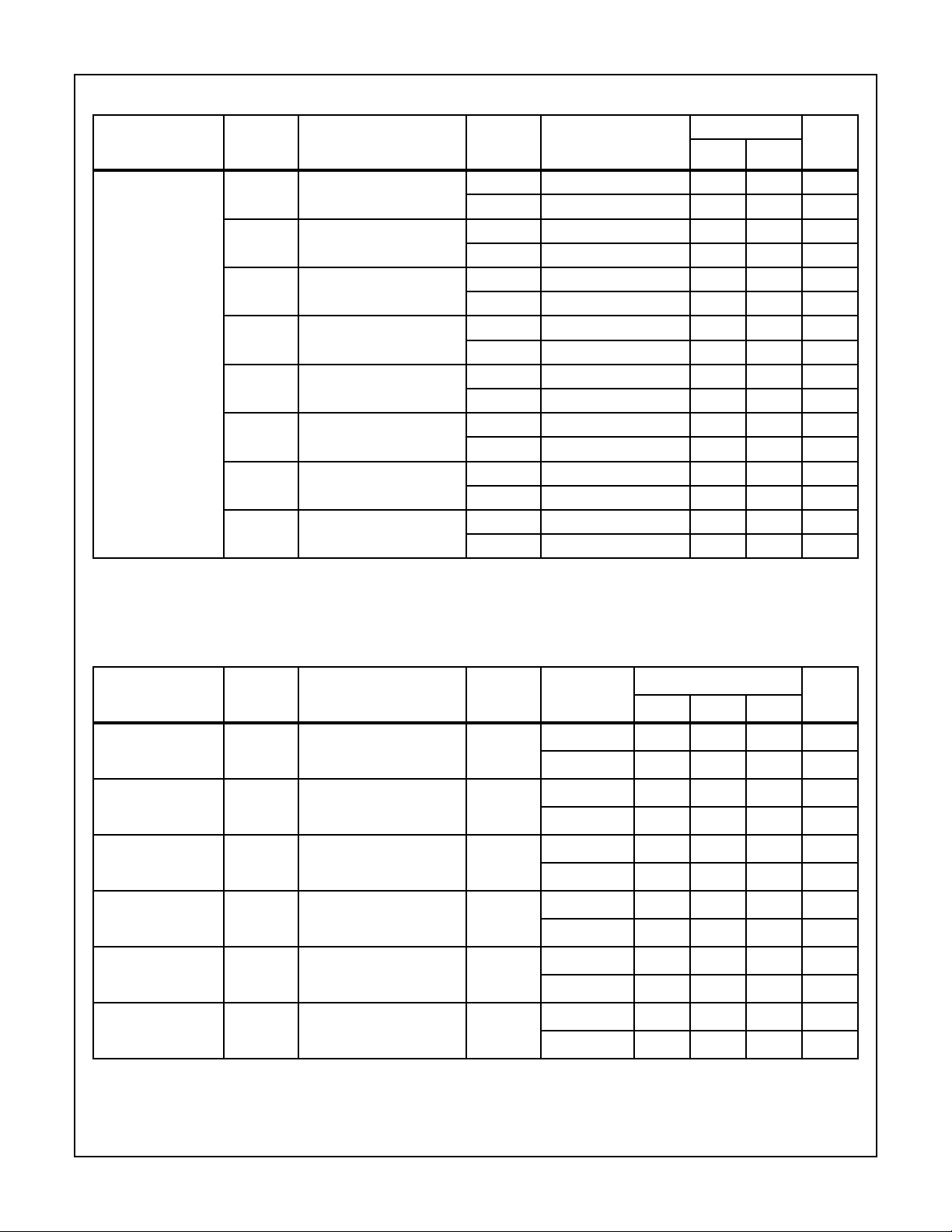
TABLE 2. AC ELECTRICAL PERFORMANCE CHARACTERISTICS
GROUP
(NOTES 1, 2)
PARAMETER SYMBOL
Propagation Delay TPHL1 VCC = 4.5V, VIH = 3.0V,
TPLH1 VCC = 4.5V, VIH = 3.0V,
TPHL2 VCC = 4.5V, VIH = 3.0V,
TPLH2 VCC = 4.5V, VIH = 3.0V,
TPZL1 VCC = 4.5V, VIH = 3.0V,
TPLZ1 VCC = 4.5V, VIH = 3.0V,
TPHZ1 VCC = 4.5V, VIH = 3.0V,
TPZH1 VCC = 4.5V, VIH = 3.0V,
NOTES:
1. All voltages referenced to device GND.
2. AC measurements assume RL = 500Ω, CL = 50pF, Input TR = TF = 3ns.
CONDITIONS
VIL = 0V
VIL = 0V
VIL = 0V
VIL = 0V
VIL = 0V
VIL = 0V
VIL = 0V
VIL = 0V
A SUB-
GROUPS TEMPERATURE
10, 11 +125oC, -55oC 2 21 ns
10, 11 +125oC, -55oC 2 20 ns
10, 11 +125oC, -55oC 2 18 ns
10, 11 +125oC, -55oC 2 19 ns
10, 11 +125oC, -55oC 2 20 ns
10, 11 +125oC, -55oC 2 18 ns
10, 11 +125oC, -55oC 2 20 ns
10, 11 +125oC, -55oC 2 18 ns
LIMITS
UNITSMIN MAX
9 +25oC 2 19 ns
9 +25oC 2 18 ns
9 +25oC 2 17 ns
9 +25oC 2 17 ns
9 +25oC 2 18 ns
9 +25oC 2 18 ns
9 +25oC 2 19 ns
9 +25oC 2 17 ns
TABLE 3. ELECTRICAL PERFORMANCE CHARACTERISTICS
LIMITS
PARAMETER SYMBOL CONDITIONS NOTE TEMP
Capacitance Power
Dissipation
Input Capacitance CIN VCC = 5.0V, VIH = 5.0V,
Output Capacitance COUT VCC = 5.0V, VIH = 5.0V,
Pulse Width Time TW VCC = 4.5V, VIH = 4.5V,
Setup Time TSU VCC = 4.5V, VIH = 4.5V,
Hold Time TH VCC = 4.5V, VIH = 4.5V,
NOTES:
1. The parameters listed in Table 3 are controlled via design or process parameters. Min and Max Limits are guaranteed but not directly
tested. These parameters are characterized upon initial design release and upon design changes which affect these characteristics.
CPD VCC = 5.0V, VIH = 5.0V,
VIL = 0V, f = 1MHz
VIL = 0V, f = 1MHz
VIL = 0V, f = 1MHz
VIL = 0V
VIL = 0V
VIL = 0V
1 +25oC - 17 - pF
+125oC - 21 - pF
1 +25oC--10pF
+125oC--10pF
1 +25oC--20pF
+125oC--20pF
1 +25oC7--ns
+125oC7--ns
1 +25oC5--ns
+125oC5--ns
1 +25oC3--ns
+125oC3--ns
UNITSMIN TYP MAX
Spec Number 518800
3
 Loading...