Intersil Corporation 82C88 Datasheet

82C88
March 1997
Features
• Compatible with Bipolar 8288
• Performance Compatible with:
- 80C86/80C88. . . . . . . . . . . . . . . . . . . . . . . . . .(5/8MHz)
- 80186/80188 . . . . . . . . . . . . . . . . . . . . . . . . . .(6/8MHz)
- 8086/8088 . . . . . . . . . . . . . . . . . . . . . . . . . . . .(5/8MHz)
- 8089
• Provides Advanced Commands for Multi-Master
Busses
• Three-State Command Outputs
• Bipolar Drive Capability
• Scaled SAJI IV CMOS Process
• Single 5V Power Supply
• Low Power Operation
- ICCSB . . . . . . . . . . . . . . . . . . . . . . . . . . . . 10µA (Max)
- ICCOP . . . . . . . . . . . . . . . . . . . . . . . . .1mA/MHz (Max)
• Operating Temperature Ranges
- C82C88 . . . . . . . . . . . . . . . . . . . . . . . . . .0
- I82C88 . . . . . . . . . . . . . . . . . . . . . . . . . -40
- M82C88 . . . . . . . . . . . . . . . . . . . . . . . -55
o
o
o
C to +125oC
C to +70oC
C to +85oC
CMOS Bus Controller
Description
The Intersil 82C88 is a high performance CMOS Bus Controller manufactured using a self-aligned silicon gate CMOS
process (Scaled SAJI IV). The 82C88 provides the control
and command timing signals for 80C86, 80C88, 8086, 8088,
8089, 80186, and 80188 based systems. The high output
drive capability of the 82C88 eliminates the need for additional bus drivers.
Static CMOS circuit design insures low operating power. The
Intersil advanced SAJI process results in performance equal
to or greater than existing equivalent products at a significant
power savings.
Ordering Information
TEMPERATURE
PART NUMBER PACKAGE
CP82C88 20 Ld PDIP 0oC to +70oC E20.3
CP82C88-10 0oC to +70oC E20.3
IP82C88 -40oC to +85oC E20.3
CS82C88 20 Ld
IS82C88 -40oC to +85oC N20.35
CD82C88 20 Ld
ID82C88 -40oC to +85oC F20.3
MD82C88/B -55oC to +125oC F20.3
8406901RA SMD# F20.3
MR82C88/B 20 Pad
84069012A SMD# J20.A
PLCC
CERDIP
CLCC
RANGE
0oC to +70oC N20.35
0oC to +70oC F20.3
-55oC to +125oC J20.A
PKG.
NO.
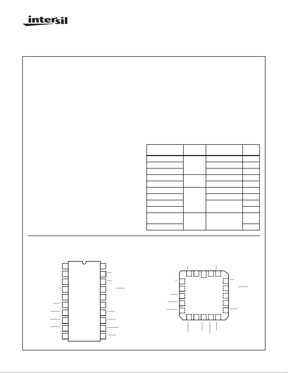
Pinouts
20 LEAD PDIP, CERDIP
TOP VIEW
1
IOB
2
CLK
3
S1
4
DT/
R
5
ALE
6
AEN
7
MRDC
MWTC
GND
8
9
10
| Copyright © Intersil Corporation 1999
AMWC
CAUTION: These devices are sensitive to electrostatic discharge; follow proper IC Handling Procedures.
http://www.intersil.com or 407-727-9207
20
V
19
S0
18
S2
17
MCE/PDEN
16
DEN
15
CEN
14
INTA
13
IORC
12
AIOWC
11
IOWC
CC
DT/
MRDC
AMWC
4-333
20 LEAD PLCC, CLCC
S1
3212019
4
R
5
ALE
6
AEN
7
8
9101112
MWTC
TOP VIEW
CLK
GND
IOWC
VCCIOB
S0
18
S2
MCE/
PDEN
DEN
CEN
INTA
AIOWC
17
16
15
14
13
IORC
File Number 2979.1

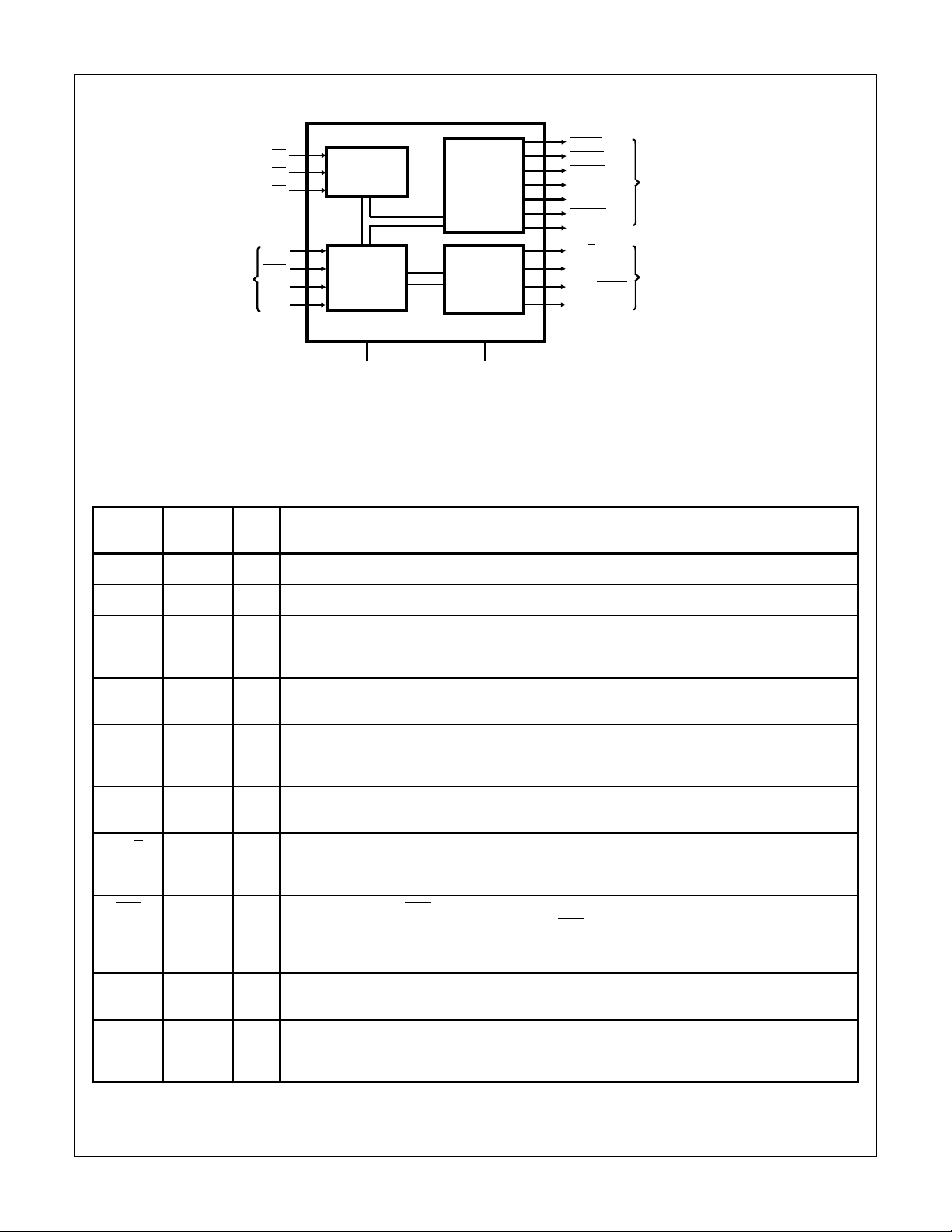
Functional Diagram
82C88
MRDC
MWTC
AMWC
IORC
IOWC
AIOWC
INTA
DT/
DEN
MCE/
ALE
CONTROL
INPUT
S0
S1
S2
CLK
AEN
CEN
IOB
STATUS
DECODER
CONTROL
LOGIC
V
CC
COMMAND
SIGNAL
GENERATOR
CONTROL
SIGNAL
GENERATOR
GND
Pin Description
PIN
SYMBOL NUMBER TYPE DESCRIPTION
V
CC
20 VCC: The +5V power supply pin. A 0.1µF capacitor between pins 10 and 20 is recommended f or decoupling.
R
PDEN
MULTIBUS
COMMAND
SIGNALS
ADDRESS LATCH,
DATA TRANSCEIVER,
AND INTERRUPT
CONTROL SIGNALS
TM
GND 10 GROUND.
S0, S1, S2 19, 3, 18 I STATUS INPUT PINS: These pins are the input pins from the 80C86, 80C88,8086/88, 8089 processors.
The 82C88 decodes these inputs to generate command and control signals at the appropriate time.
When Status pins are not in use (passive), command outputs are held HIGH (See Table1).
CLK 2 I CLOCK: This is a CMOS compatible input which receives a clock signal from the 82C84A or 82C85 clock
generator and serves to establish when command/control signals are generated.
ALE 5 O ADDRESS LATCH ENABLE: This signal serves to strobe an address into the address latches. This sig-
nal is active HIGH and latching occurs on the falling (HIGH to LOW) transition. ALE is intended for use
with transparent D type latches, such as the 82C82 and 82C83H.
DEN 16 O DATA ENABLE: This signal serves to enable data transceivers onto either the local or system data bus.
This signal is active HIGH.
DT/R 4 O DATA TRANSMIT/RECEIVE: This signal establishes the direction of data flow through the transceivers.
A HIGH on this line indicates Transmit (write to I/O or memory) and a LOW indicates Receive (read from
I/O or memory).
AEN 6 I ADDRESS ENABLE: AEN enables command outputs of the 82C88 Bus Controller a minimum of 110ns
(250ns maximum) after it becomes active (LOW). AEN going inactive immediately three-states the command output drivers. AEN does not affect the I/O command lines if the 82C88 is in the I/O Bus mode
(IOB tied HIGH).
CEN 15 I COMMAND ENABLE: When this signal is LOW all 82C88 command outputs and the DEN and PDEN con-
trol outputs are forced to their Inactive state. When this signal is HIGH, these same outputs are enabled.
IOB 1 I INPUT/OUTPUT BUS MODE: When the IOB pin is strapped HIGH, the 82C88 functions in the I/O Bus
mode. When it is strapped LOW, the 82C88 functions in the System Bus mode (See I/O Bus and System
Bus sections).
Intel™ is a Registered Trademark of Intel Corporation
4-334

82C88
Pin Description
PIN
SYMBOL NUMBER TYPE DESCRIPTION
AIOWC 12 O ADVANCED I/O WRITE COMMAND: The AIOWC issues an I/O Write Command earlier in the machine
IOWC 11 O I/O WRITE COMMAND: This command line instructs an I/O device to read the data on the data bus. The
IORC 13 O I/O READ COMMAND: This command line instructs an I/O device to drive its data onto the data bus. This
AMWC 8 O ADVANCED MEMORY WRITE COMMAND: The AMWC issues a memory write command earlier in the
MWTC 9 O MEMORY WRITE COMMAND: This command line instructs the memory to record the data present on
MRDC 7 O MEMORY READ COMMAND: This command line instructs the memory to drive its data onto the data
INTA 14 O INTERRUPT ACKNOWLEDGE: This command line tells an interrupting device that its interrupt has been
MCE/PDEN 17 O This is a dual function pin. MCE (IOB IS TIED LOW) Master Cascade Enable occurs during an interrupt
(Continued)
cycle to give I/O devices an early indication of a write instruction. Its timing is the same as a read command signal. AIOWC is active LOW.
signal is active LOW.
signal is active LOW.
machine cycle to give memory devices an early indication of a write instruction. Its timing is the same as
a read command signal. AMWC is active LOW.
the data bus. This signal is active LOW.
bus. MRDC is active LOW.
acknowledged and that it should drive vectoring information onto the data bus. This signal is active LOW.
sequence and serves to read a Cascade Address from a master 82C59A Priority Interrupt Controller onto
the data bus. The MCE signal is active HIGH. PDEN (IOB IS TIED HIGH): Peripheral Data Enable enables
the data bus transceiver for the I/O bus that DEN performs for the system bus. PDEN is active LOW.
Functional Description
The command logic decodes the three 80C86, 8086, 80C88,
8088, 80186, 80188 or 8089 status lines (
determine what command is to be issued (see Table 1).
TABLE 1. COMMAND DECODE DEFINITION
S2 S1 S0 PROCESSOR STATE
0 0 0 Interrupt Acknowledge INTA
0 0 1 Read I/O Port IORC
0 1 0 Write I/O Port IOWC, AIOWC
0 1 1 Halt None
1 0 0 Code Access MRDC
1 0 1 Read Memory MRDC
1 1 0 Write Memory MWTC, AMWC
1 1 1 Passive None
I/O Bus Mode
The 82C88 is in the I/O Bus mode if the IOB pin is strapped
HIGH. In the I/O Bus mode, all I/O command lines IORC,
IOWC, AIOWC, INTA) are always enabled (i.e., not dependent on
AEN). When an I/O command is initiated by the pro-
S0, S1, S2) to
82C88
COMMAND
cessor, the 82C88 immediately activates the command lines
using
PDEN and DT/R to control the I/O bus transceiver. The
I/O command lines should not be used to control the system
bus in this configuration because no arbitration is present.
This mode allows one 82C88 Bus Controller to handle two
external busses. No waiting is involved when the CPU wants
to gain access to the I/O bus. Normal memory access
requires a “Bus Ready” signal (
AEN LOW) before it will proceed. It is advantageous to use the IOB mode if I/O or
peripherals dedicated to one processor exist in a multi-processor system.
System Bus Mode
The 82C88 is in the System Bus mode if the IOB pin is
strapped LOW. In this mode, no command is issued until a
specified time period after the
AEN line is activated (LOW).
This mode assumes bus arbitration logic will inform the bus
controller (on the
AEN line) when the bus is free for use.
Both memory and I/O commands wait for bus arbitration.
This mode is used when only one bus exists. Here, both I/O
and memory are shared by more than one processor.
Command Outputs
The advanced write commands are made available to initiate
write procedures early in the machine cycle. This signal can
be used to prevent the processor from entering an unnecessary wait state.
4-335
 Loading...