Intersil Corporation 82C87H Datasheet

82C87H
March 1997
Features
• Full Eight Bit Bi-Directional Bus Interface
• Industry Standard 8287 Compatible Pinout
• High Drive Capability
- B Side I
- A Side I
• Three-State Inverting Outputs
• Propagation Delay . . . . . . . . . . . . . . . . . . . . . 35ns Max.
• Gated Inputs
- Reduce Operating Power
- Eliminate the Need for Pull-Up Resistors
• Single 5V Power Supply
• Low Power Operation . . . . . . . . . . . . . . . ICCSB = 10µA
• Operating Temperature Range
- C82C87H . . . . . . . . . . . . . . . . . . . . . . . . . 0
- I82C87H. . . . . . . . . . . . . . . . . . . . . . . . -40
- M82C87H. . . . . . . . . . . . . . . . . . . . . . -55
. . . . . . . . . . . . . . . . . . . . . . . . . . . . . . 20mA
OL
. . . . . . . . . . . . . . . . . . . . . . . . . . . . . . 12mA
OL
o
C to +70oC
o
C to +85oC
o
C to +125oC
CMOS Octal Inverting Bus Transceiver
Description
The Intersil 82C87H is a high performance CMOS Octal
Transceiver manufactured using a self-aligned silicon gate
CMOS process (Scaled SAJI IV). The 82C87H provides a full
eight-bit bi-directional bus interface in a 20 pin package. The
Transmit (T) control determines the data direction. The active
low output enable (
80C86, 80C88 and other microprocessors. The 82C87H has
gated inputs, eliminating the need for pull-up/pull-down resistors and reducing overall system operating power dissipation.
The 82C87H provides inverted data at the outputs.
Ordering Information
PART NUMBERS
CP82C87H-5 CP82C87H 20 Ld
IP82C87H-5 IP82C87H -40oC to +85oC E20.3
CS82C87H-5 CS82C87H 20 Ld
IS82C87H-5 IS82C87H -40oC to +85oC N20.35
CD82C87H-5 CD82C87H 20 Ld
ID82C87H-5 ID82C87H -40oC to +85oC F20.3
MD82C87H-5/B - -55oC to
59628757702RA
MR82C87H-5/B - 20 Pad
596287577022A
OE) permits simple interface to the
PACK-
AGE
PDIP
PLCC
CERDIP
- SMD # F20.3
CLCC
- SMD # J20.A
TEMP.
RANGE
0oC to +70oC E20.3
0oC to +70oC N20.35
0oC to +70oC F20.3
+125oC
-55oC to
+125oC
PKG.
NO.5MHz 8MHz
F20.3
J20.A
CAUTION: These devices are sensitive to electrostatic discharge; follow proper IC Handling Procedures.
http://www.intersil.com or 407-727-9207
| Copyright © Intersil Corporation 1999
4-325
File Number 2978.1

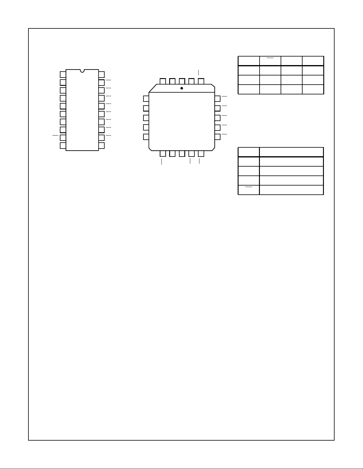
Pinouts
82C87H82C87H
82C87H (PDIP, CERDIP)
TOP VIEW
1
A0
2
A1
3
A2
4
A3
5
A4
6
A5
A6
7
8
A7
9
OE
10
GND
82C87H (PLCC, CLCC)
TOP VIEW
A2
20
V
CC
B0
19
18
B1
17
B2
16
B3
15
B4
14
B5
13
B6
12
B7
T
11
A3
A4
A5
A6
A7
4
5
6
7
8
A1
9
10 11 12 13
OE
GND
A0
CC
B0
V
193 2 201
18
17
16
15
14
H = Logic One
B1
L = Logic Zero
B2
I = Input Mode
O = Output Mode
B3
X = Don’t Care
B4
Hi-Z = High Impedance
B5
PIN DESCRIPTION
T
B7
B6
A0-A7Local Bus Data I/O Pins
B0-B7System Bus Data I/O Pins
TRUTH TABLE
T OE A B
X H Hi-Z Hi-Z
HL IO
LLOI
PIN NAMES
T Transmit Control Input
OE Active Low Output Enable
4-326

82C87H
82C87H
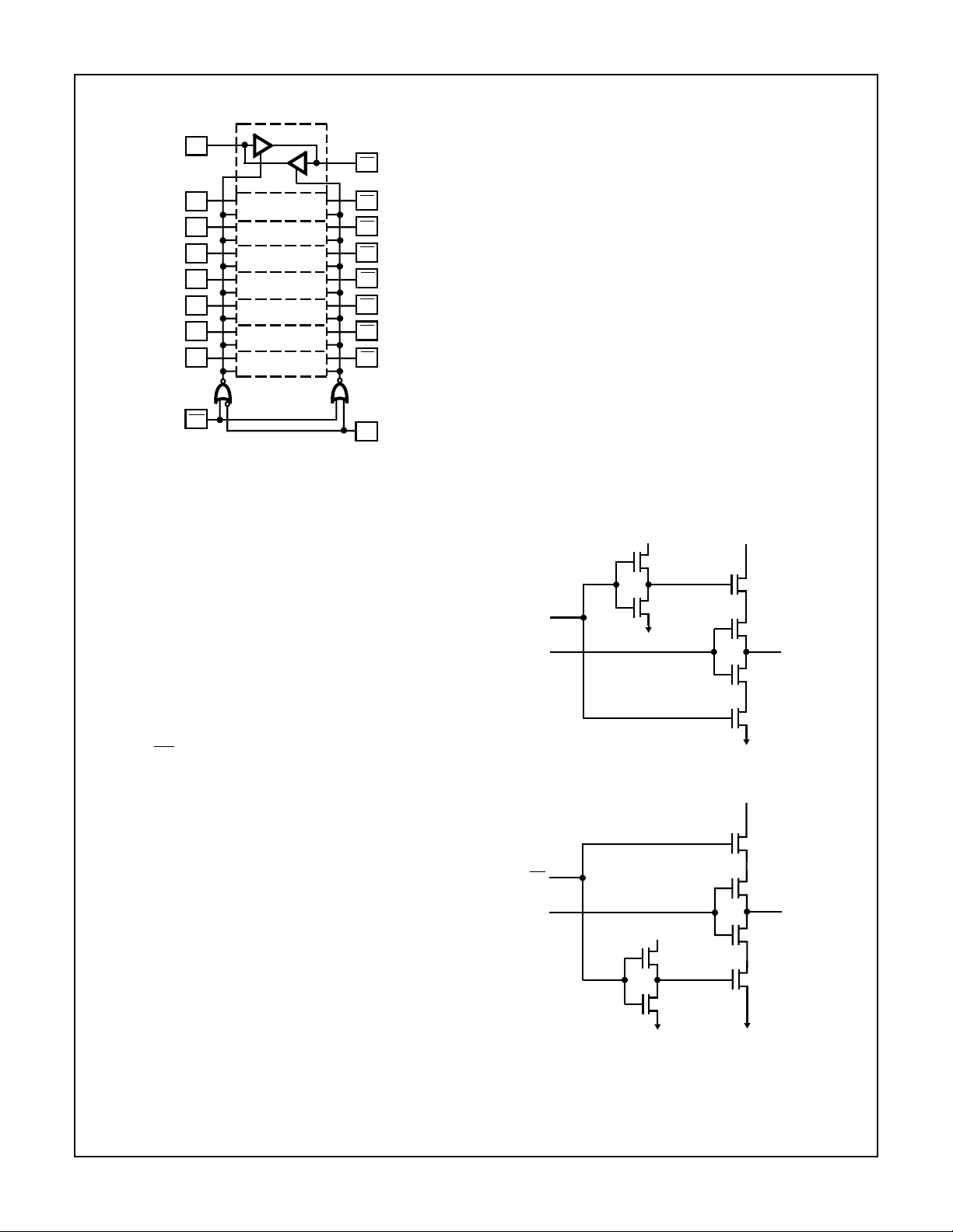
Functional Diagram
A0
B0
A1
A2
A3
A4
A5
A6
A7
OE
B1
B2
B3
B4
B5
B6
B7
T
Gated Inputs
During normal system operation of a latch, signals on the
bus at the device inputs will become high impedance or
make transitions unrelated to the operation of the latch.
These unrelated input transitions switch the input circuitry
and typically cause an increase in power dissipation in
CMOS devices by creating a low resistance path between
V
and GND when the signal is at or near the input switch-
CC
ing threshold. Additionally, if the driving signal becomes high
impedance (“float” condition), it could create an indeterminate logic state at the inputs and cause a disruption in
device operation.
Decoupling Capacitors
The transient current required to charge and discharge the
300pF load capacitance specified in the 82C86H/87H data
sheet is determined by:
ICLdv dt⁄()=
Assuming that all outputs change state at the same time and
that dv/dt is constant;
VCC 80%×()
------------------------------------ -
=
IC
L
tR tF⁄
where tR = 20ns, V
= 5.0V, CL = 300pF on each eight out-
CC
puts.
12–
I 80 300 10
480mA=
××()5.0V 0.8×()20 109–×()⁄×=
This current spike may cause a large negative voltage spike on
V
which could cause improper operation of the device. To fil-
CC
ter out this noise, it is recommended that a 0.1µF ceramic disc
capacitor be placed between V
and GND at each device,
CC
with placement being as near to the device as possible.
STB
DATA IN
V
CC
P
N
V
CC
P
P
N
(EQ. 4)
(EQ. 5)
(EQ. 6)
INTERNAL
DAT A
The Intersil 82C8X series of bus drivers eliminates these
conditions by turning off data inputs when data is latched
(STB = logic zero for the 82C82/83H) and when the de vice is
disabled (
inputs disconnect the input circuitry from the V
OE = logic one for the 82C87H/87H). These gated
and
CC
ground power supply pins by turning off the upper P-Channel and lower N-Channel (See Figures 1 and 2). No current
flow from V
to GND occurs during input transitions and
CC
invalid logic states from floating inputs are not transmitted.
The next stage is held to a valid logic level internal to the
device.
D.C. input voltage levels can also cause an increase in ICC if
these input levels approach the minimum V
V
conditions. This is due to the operation of the input cir-
IL
or maximum
IH
cuitry in its linear operating region (partially conducting
state). The 82C8X series gated inputs mean that this condition will occur only during the time the device is in the transparent mode (STB = logic one). ICC remains below the
maximum ICC standby specification of 10µA during the time
inputs are disabled, thereby greatly reducing the average
power dissipation of the 82C8X series devices.
OE
DATA IN
N
FIGURE 3. 82C82/83H
V
CC
P
P
V
CC
P
N
FIGURE 4. 82C86H/87H GATED INPUTS
N
N
INTERNAL
DAT A
4-327
 Loading...