Intersil Corporation 82C52 Datasheet
82C52
March 1997
Features
• Single Chip UART/BRG
• DC to 16MHz (1M Baud) Operation
• Crystal or External Clock Input
• On-Chip Baud Rate Generator - 72 Selectable Baud
Rates
• Interrupt Mode with Mask Capability
• Microprocessor Bus Oriented Interface
• 80C86 Compatible
• Single +5V Power Supply
• Low Power Operation . . . . . . . . . . . . . . . 1mA/MHz Typ
• Modem Interface
• Line Break Generation and Detection
• Operating Temperature Range:
o
- C82C52 . . . . . . . . . . . . . . . . . . . . . . . . . .0
- I82C52 . . . . . . . . . . . . . . . . . . . . . . . . . -40
- M82C52 . . . . . . . . . . . . . . . . . . . . . . . -55
C to +70oC
o
C to +85oC
o
C to +125oC
CMOS Serial Controller Interface
Description
The Intersil 82C52 is a high performance programmable
Universal Asynchronous Receiver/Transmitter (UART) and
Baud Rate Generator (BRG) on a single chip. Utilizing the
Intersil advanced Scaled SAJI IV CMOS process, the 82C52
will support data rates up to 1M baud asynchronously with a
16X clock (16MHz clock frequency).
The on-chip Baud Rate Generator can be programmed for
any one of 72 different baud rates using a single industry
standard crystal or external frequency source. A unique prescale divide circuit has been designed to provide standard
RS-232-C baud rates when using any one of three industry
standard crystals (1.8432MHz, 2.4576MHz, or 3.072MHz).
A programmable buffered clock output (CO) is available and
can be programmed to provide either a buffered oscillator or
16X baud rate clock for general purpose system usage.
Ordering Information
TEMPERA TURE
PACKAGE
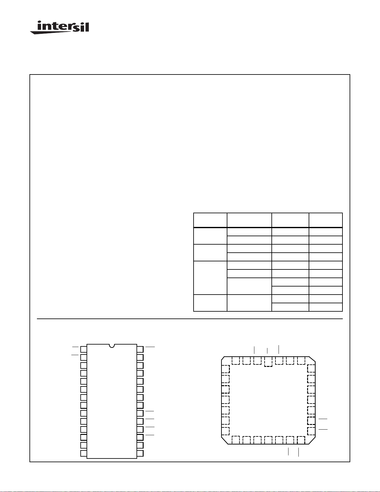
PDIP 0oC to +70oC CP82C52 E28.6
PLCC 0oC to +70oC CS82C52 N28.45
CERDIP 0oC to +70oC CD82C52 F28.6
SMD# 8501501XA F28.6
CLCC -55oC to +125oC MR82C52/B J28.A
SMD# 85015013A J28.A
RANGE 1M BAUD PKG. NO.
-40oC to +85oC IP82C52 E28.6
-40oC to +85oC IS82C52 N28.45
-40oC to +85oC ID82C52 F28.6
-55oC to +125oC MD82C52/B F28.6
Pinouts
82C52 (PDIP, CERDIP)
TOP VIEW
RD
1
WR
2
3
D0
4
D1
D2
5
6
D3
7
D4
8
D5
9
D6
10
D7
11
A0
12
A1
13
IX
14
OX
CAUTION: These devices are sensitive to electrostatic discharge; follow proper IC Handling Procedures.
http://www.intersil.com or 407-727-9207
| Copyright © Intersil Corporation 1999
CSO
28
27
VCC
26
DR
25
SDI
24
INTR
23
RST
22
TBRE
21
CO
20
RTS
19
DTR
18
DSR
17
CTS
16
GND
15
SDO
D2
D3
D4
D5
D6
D7
A0
5
6
7
8
9
10
11
5-1
82C52 (PLCC, CLCC)
TOP VIEW
RD
WR
14 15 16 17 1812 13
OX
SDO
A1
D1
D0
3 2 14
IX
VCC
CTS
DR
25
24
23
22
21
20
19
DSR
CSO
28 27 26
GND
File Number 2950.1
SDI
INTR
RST
TBRE
CO
RTS
DTR
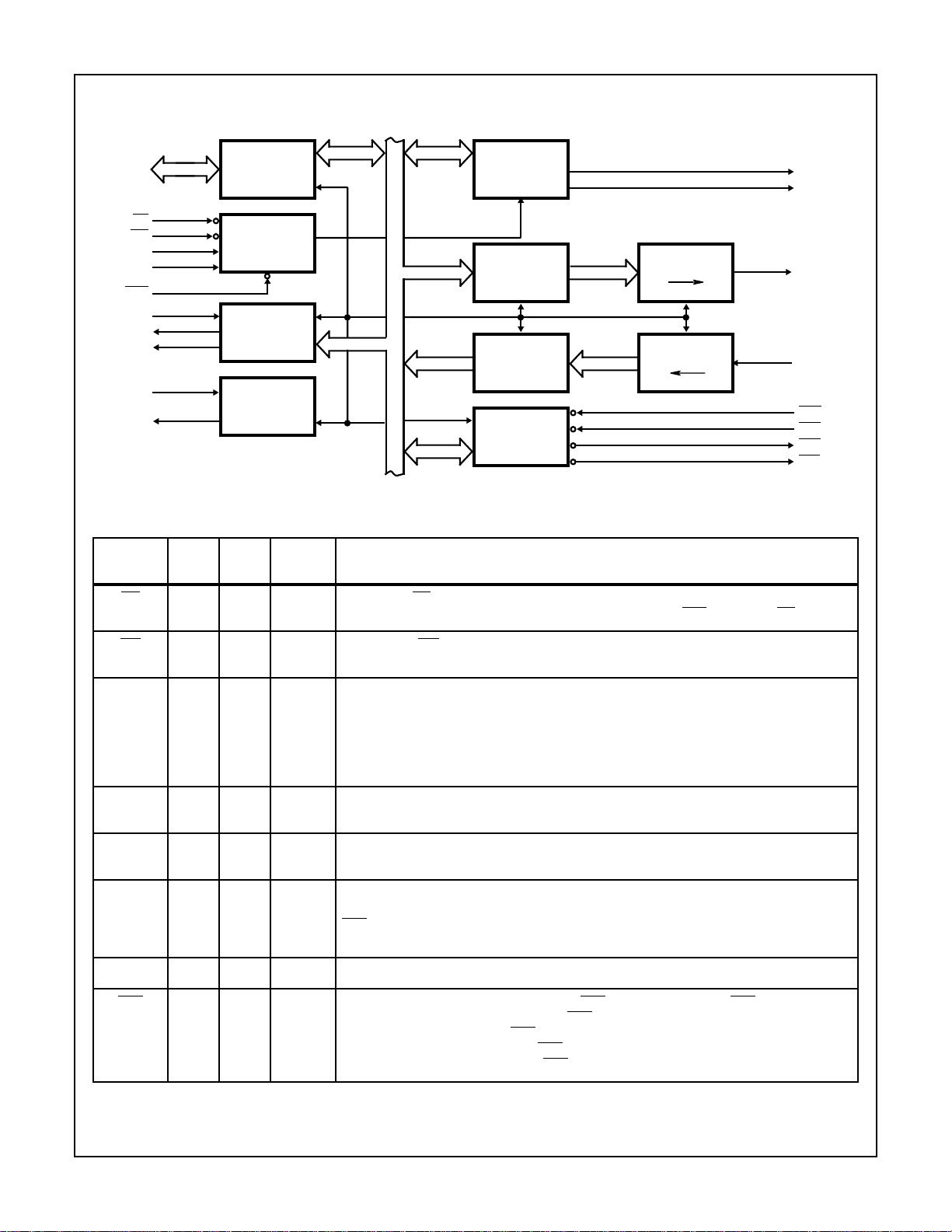
Block Diagram
82C52
UART
CONTROL AND
STATUS
REGISTERS
TRANSMITTER
BUFFER
REGISTER
RECEIVER
BUFFER
REGISTER
MODEM
CONTROL AND
STATUS
REGISTERS
TRANSMITTER
REGISTER
P
RECEIVER
REGISTER
P
S
S
22
26
15
25
18
17
19
20
D0-D7
RD
WR
A0
A1
CSO
OX
CO
RST
INTR
3 - 10
1
2
11
12
28
13
IX
14
21
23
24
DAT A
BUS
BUFFER
READ/WRITE
CONTROL
LOGIC
PROGRAM-
MABLE
BOUD RATE
GENERATOR
CONTROL
LOGIC
INTERNAL DATA BUS
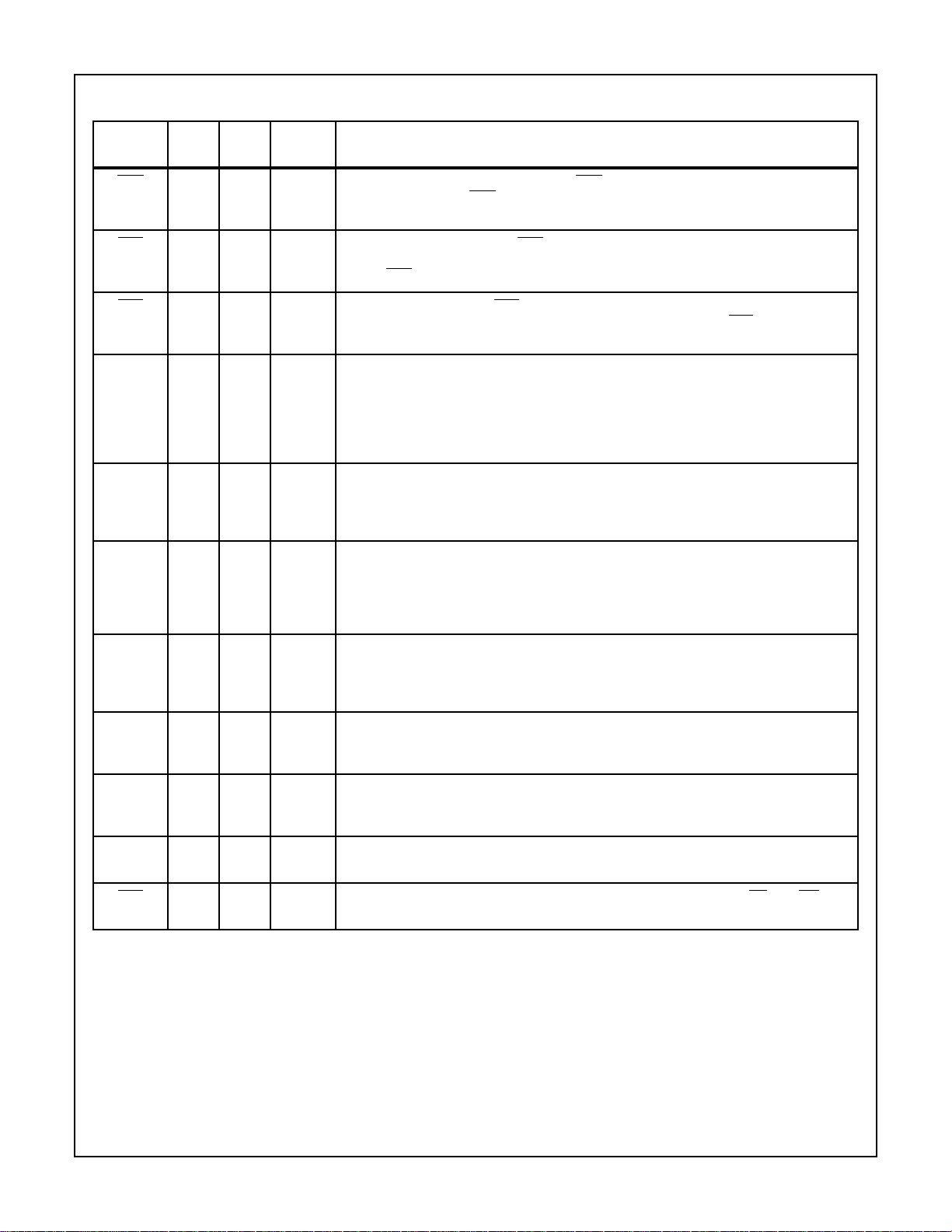
Pin Description
PIN
SYMBOL
NO. TYPE
RD 1 I Low READ: The RD input causes the 82C52 to output data to the data bus (D0-D7). The data
ACTIVE
LEVEL DESCRIPTION
output depends upon the state of the address inputs (A0-A1). CS0 enables the RD input.
TBRE
DR
SDO
SDI
DSR
CTS
DTR
RTS
WR 2 I Low WRITE: The WR input causes data from the data bus (D0-D7) to be input to the 82C52.
Addressing and chip select action is the same as for read operations.
D0-D7 3-10 I/O High DATA BITS 0-7: The Data Bus provides eight, three-state input/output lines for the transfer of
data, control and status information between the 82C52 and the CPU. For character formats
of less than 8 bits, the corresponding D7, D6 and D5 are considered “don't cares” for data
WRITE operations and are 0 for data READ operations. These lines are normally in a high
impedance state except during read operations. D0 is the Least Significant Bit (LSB) and is the
first serial data bit to be received or transmitted.
A0, A1 11, 12 I High ADDRESS INPUTS: The address lines select the various internal registers dur ing CPU bus
operations.
IX, OX 13, 14 I/O CRYSTAL/CLOCK: Crystal connections for the internal Baud Rate Generator. IX can also be
used as an external clock input in which case OX should be left open.
SDO 15 O High SERIAL D ATA OUTPUT: Serial data output from the 82C52 transmitter circuitry. A Mark (1) is
a logic one (high) and Space (0) is logic zero (low). SD0 is held in the Mark condition when
CTS is false, when RST is true, when the Transmitter Register is empty, or when in the Loop
Mode.
GND 16 Low GROUND: Power supply ground connection.
CTS 17 I Low CLEAR TO SEND: The logical state of the CTS line is reflected in the CTS bit of the Modem
Status Register. Any change of state in CTS causes INTR to be set true when INTEN and
MIEN are true. A false lev el onCTS will inhibit transmission of data on the SD0 output and will
hold SD0 in the Mark (high) state. If CTS goes false during transmission, the current character
being transmitted will be completed. CTS does not affect Loop Mode operation.
5-2
82C52
Pin Description
PIN
SYMBOL
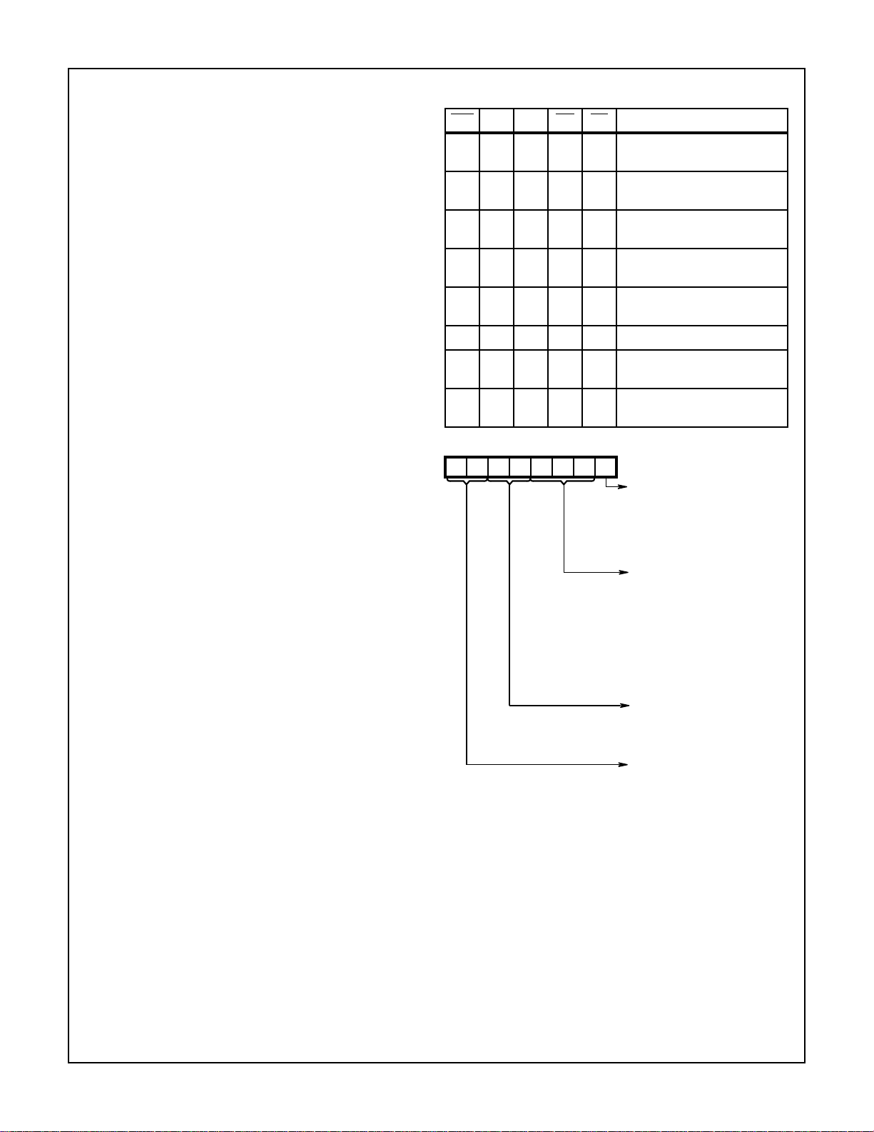
DSR 18 I Low DA TA SET READ Y : The logical state of theDSR line is reflected in the Modem Status Register.
DTR 19 O Low DATA TERMINAL READY: The DTR signal can be set (low) by writing a logic 1 to the appro-
RTS 20 O Low REQUEST TO SEND: The RTS signal can be set (low) by writing a logic 1 to the appropriate
CO 21 O CLOCK OUT: This output is user programmable to provide either a buffered IX output or a
TBRE 22 O High TRANSMITTER BUFFER REGISTER EMPTY: The TBRE output is set (high) whenever the
NO. TYPE
(Continued)
ACTIVE
LEVEL DESCRIPTION
Any change of state of DSR will cause INTR to be set if INTEN and MIEN are true. The state
of this signal does not affect any other circuitry within the 82C52.
priate bit in the Modem Control Register (MCR). This signal is cleared (high) by writing a logic
0 in the DTR bit in the MCR or whenever a reset (RST = high) is applied to the 82C52.
bit in the MCR. This signal is cleared (high) by writing a logic 0 to the RTS bit in the MCR or
whenever a reset (RST = high) is applied to the 82C52.
buffered Baud Rate Generator (16X) clock output. The buffered IX (Crystal or external clock
source) output is provided when the Baud Rate Select Register (BRSR) bit 7 is set to a zero.
Writing a logic one to BRSR bit 7 causes the CO output to provide a buffered version of the
internal Baud Rate Generator clock which operates at sixteen times the programmed baud
rate. On reset D7 (CO select) is reset to 0.
T r ansmitter Buffer Register (TBR) has tr ansferred its data to the Transmit Register. Application
of a reset (RST) to the 82C52 will also set the TBRE output. TBRE is cleared (low) whenever
data is written to the TBR.
RST 23 I High RESET: The RST input forces the 82C52 into an “Idle” mode in which all serial data activities
are suspended. The Modem Control Register (MCR) along with its associated outputs are
cleared. The UART Status Register (USR) is cleared except for the TBRE and TC bits, which
are set. The 82C52 remains in an “Idle” state until programmed to resume serial data activities.
The RST input is a Schmitt triggered input.
INTR 24 O High INTERRUPT REQUEST: The INTR output is enabled by the INTEN bit in the Modem Control
Register (MCR). The MIEN bit selectively enables modem status changes to provide an input
to the INTR logic. Figure 9 in Design Information shows the overall relationship of these interrupt control signals.
SDI 25 I High SERIAL DATA INPUT: Serial data input to the 82C52 receiver circuits. A Mark (1) is high, and
a Space (0) is low. Data inputs on SDI are disabled when operating in the loop mode or when
RST is true.
DR 26 O High DATA READY: A true level indicates that a character has been received, transferred to the
RBR, and is ready for transfer to the CPU. DR is reset on a data READ of the Receiver Buffer
Register (RBR) or when RST is true.
V
CC
CS0 28 I Low CHIP SELECT: The chip select input acts as an enable signal for the RD and WR input
27 High VCC: +5V positive power supply pin. A 0.1µF decoupling capacitor from VCC (Pin 27) to GND
(Pin 16) is recommended.
signals.
5-3
82C52
Reset
During and after power-up, the 82C52 Reset Input (RST)
must be held high for at least two IX clock cycles in order to
initialize and drive the 82C52 circuits to an idle mode until
proper programming can be done. A high on RST causes
the following events to occur
• Resets the internal Baud Rate Generator (BRG) circuit
clock counters and bit counters. The Baud Rate Select
Register (BRSR) is not affected (except for bit 7 which is
reset to 0).
• Clears the UART Status Register (USR) except for
Transmission Complete (TC) and Transmit Buffer Register
Empty (TBRE) which are set. The Modem Control
Register (MCR) is also cleared. All of the discrete lines,
memory elements and miscellaneous logic associated
with these register bits are also cleared or turned off. Note
that the UART Control Register (UCR) is not affected.
Following removal of the reset condition (RST = low), the
82C52 remains in the idle mode until programmed to its
desired system configuration.
Programming The 82C52
The complete functional definition of the 82C52 is
programmed by the systems software. A set of control w ords
(UCR, BRSR and MCR) must be sent out by the CPU to
initialize the 82C52 to support the desired communication
format. These control words will program the character
length, number of stop bits, even/odd/no parity, baud rate,
etc. Once programmed, the 82C52 is ready to perform its
communication functions.
The control registers can be written to in any order. However,
the MCR should be written to last because it controls the
interrupt enables, modem control outputs and the receiver
enable bit. Once the 82C52 is programmed and operational,
these registers can be updated any time the 82C52 is not
immediately transmitting or receiving data.
Table 1. Shows the control signals required to access 82C52
internal registers.
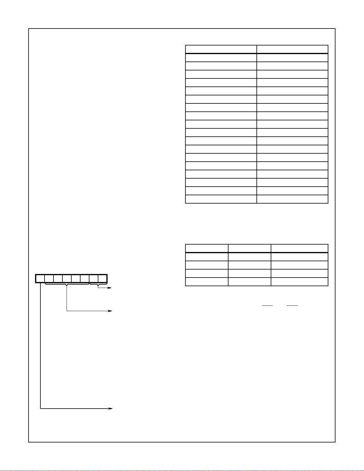
UART Control Register (UCR)
The UCR is a write only register which configures the UART
transmitter and receiver circuits. Data bits D7 and D6 are not
used but should always be set to a logic zero (0) in order to
insure software compatibility with future product upgrades.
During the Echo Mode, the transmitter always repeats the
received word and parity, even when the UCR is
programmed with different or no parity. See Figure 1.
TABLE 1.
CS0 A1 A0 WR RD OPERATION
00001Data Bus → Transmitter Buffer
Register (TBR)
00010Receiver Buffer Register
(RBR) → Data Bus
00101Data Bus → UART Control
Register (UCR)
00110UART Status Register
(USR) → Data Bus
01001Data Bus → Modem Control
Register (MCR)
01010MCR→ Data Bus
01101Data Bus → Bit Rate Select
Register (BRSR)
01110Modem Status Register
(MSR) → Data Bus
D7 D6 D5 D4 D3 D2 D1 D0
Stop Bit
Select
Parity
Control
Word
Length
Select
Reserved Set to 00 for Future
FIGURE 1. UCR
0 = 1 Stop Bits
1 = 1.5 Stop Bits (Tx)
and 1 Stop Bit (Rx)
If 5 Data Bits Selected
1 = 2 Stop Bits for 6, 7
or 8 Data Bits Selected
000 = Tx and Rx Even
001 = Tx and Rx Odd
010 = Tx Even, Rx
Odd
011 = Tx Odd, Rx
Even
100 = Tx Even, Rx
Check Disabled
101 = Tx Odd, Rx
Check Disabled
11X = Generation and
Check Disabled
00 = 5 Bits
01 = 6 Bits
10 = 7 Bits
11 = 8 Bits
Product Upgrade
Compatibility
5-4
82C52
Baud Rate Select Register (BRSR)
The 82C52 is designed to operate with a single crystal or
external clock driving the IX input pin. The Baud Rate Select
Register is used to select the divide ratio (one of 72) for the
internal Baud Rate Generator circuitry. The internal circuitry
is separated into two separate counters, a Prescaler and a
Divisor Select. The Prescaler can be set to any one of four
division rates, ÷1, ÷3, ÷4, or ÷5.
The Prescaler design has been optimized to provide
standard baud rates using any one of three popular crystal
frequencies. By using one of these common system clock
frequencies, 1.8432MHz, 2.4576MHz or 3.072MHz and
Prescaler divide ratios of ÷3, ÷4, or ÷5 respectively, the
Prescaler output will provide a constant 614.4KHz. When
this frequency is further divided by the Divisor Select
counter, any of the standard baud rates from 50 Baud to
38.4Kbaud can be selected (see Table 2). Non-standard
baud rates up to 1Mbaud can be selected by using different
input frequencies (crystal or an external frequency input up
to 16MHz) and/or different Prescaler and Divisor Select
ratios.
Regardless of the baud rate, the baud rate generator
provides a clock which is 16 times the desired baud rate. F or
example, in order to operate at a 1Mbaud data rate, a
16MHz crystal, a Prescale rate of ÷1, and a Divisor Select
rate of “external” would be used. This would provide a
16MHz clock as the output of the Baud Rate Generator to
the Transmitter and Receiver circuits.
The CO select bit in the BRSR selects whether a buffered
version of the external frequency input (IX input) or the Baud
Rate Generator output (16x baud rate clock) will be output
on the CO output (pin 21). The Baud Rate Generator output
will always be a 50% nominal duty cycle except when “external” is selected and the Prescaler is set to ÷3 or ÷5.
D7 D6 D5 D4 D3 D2 D1 D0
Prescaler
Select
Divisor
Select
CO
Select
FIGURE 2. BRSR
00 = ÷ 1
01 = ÷ 3
10 = ÷ 4
11 = ÷ 5
00000 = ÷ 2
00001 = ÷ 4
00010 = ÷ 16/3
00011 = ÷ 8
00100 = ÷ 32/3
00101 = ÷ 16
00110 = ÷ 58/3
00111 = ÷ 22
01000 = ÷ 32
01001 = ÷ 64
01010 = ÷ 128
01011 = ÷ 192
01100 = ÷ 256
01101 = ÷ 288
01110 = ÷ 352
01111 = ÷ 512
10000 = ÷ 768
11111 = External (÷ 1)
0 = IX Output
1 = Brg Output (On
Reset, D7 (CO Select)
is Reset to 0)
TABLE 2.
BAUD RATE DIVISOR
38.4K External
19.2K 2
9600 4
7200 16/3
4800 8
3600 32/3
2400 16
2000† 58/3
1800† 22
1200 32
600 64
300 128
200 192
150 256
134.5† 288
110† 352
75 512
50 768
NOTE: These baud rates are based upon the following input
frequency/ Prescale divisor combinations.
1.8432MHz and Prescale = ÷ 3
2.4576MHz and Prescale = ÷ 4
3.072MHZ and Prescale = ÷ 5
† All baud rates are exact except for:
BAUD RATE ACTUAL PERCENT ERROR
1800 1745.45 3.03%
2000 1986.2 0.69%
134.5 133.33 0.87%
110 109.09 0.83%
Modem Control Register
The MCR is a general purpose control register which can be
written to and read from. The
RTS and DTR outputs are
directly controlled by their associated bits in this register.
Note that a logic one asserts a true logic level (low) at these
output pins. The Interrupt Enable (INTEN) bit is the overall
control for the INTR output pin. When INTEN is false, INTR
is held false (low).
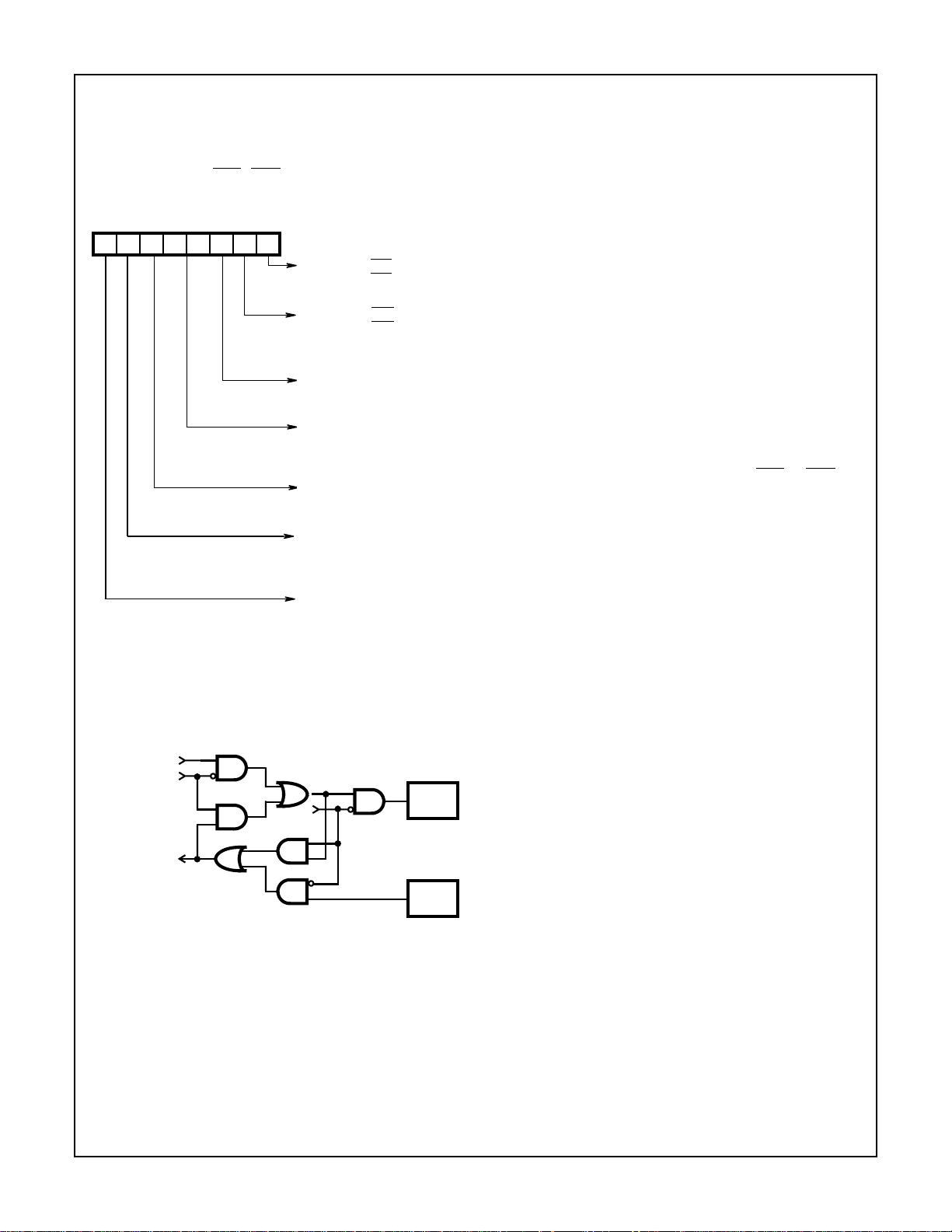
The Operating Mode bits configure the 82C52 into one of
four possible modes. “Normal” configures the 82C52 for normal full or half duplex communications. “Transmit Break”'
enables the transmitter to only transmit break characters
(Start, Data and Stop bits all are logic zero). The Echo Mode
causes any data that is received on the SDI input pin to be
retransmitted on the SDO output pin. Note that this output is
a buffered version of the data seen on the SDI input and is
not a resynchronized output. Also note that normal UART
transmission via the Transmitter Register is disabled when
operating in the Echo mode (see Figure 4). The Loop Test
Mode internally routes transmitted data to the receiver
circuitry for the purpose of self test. The transmit data is
5-5
82C52
disabled from the SDO output pin. The Receiver Enable bit
gates off the input to the receiver circuitry when in the false
state.
Modem Interrupt Enable will permit any change in modem
status line inputs (
CTS, DSR) to cause an interrupt when
this bit is enabled. Bit D7 must always be written to with a
logic zero to insure correct 82C52 operation.
D7 D6 D5 D4 D3 D2 D1 D0
Request
to Send
(RTS)
Data
Terminal
Ready
(DTR)
Interrupt
Enable
(INTEN)
Mode
Select
Receiver
Enable
(REN)
Modem
Interrupt
Enable
(MIEN)
Must be Set to a Logic 0 for
Normal 82C52 Operation
† See Modem Status Register description for a description of
register flag images with respect to output pins.
FIGURE 3. MCR
0 = RTS Output High†
1 =
RTS Output Low
DTR Output High
0 =
1 =
DTR Output Low
1 = Interrupts Enabled
0 = interrupts Disabled
00 = Normal
01 = Transmit Break
10 = Echo Mode
11 = Loop Test Mode
0 = Not Enabled
1 = Enabled
0 = Not Enabled
1 = Enabled
Three error flags OE, FE and PE report the status of any
error conditions detected in the receiver circuitry. These
error flags are updated with every character received during
reception of the stop bits. The Overrun Error (OE) indicates
that a character in the Receiver Register has been received
and cannot be transferred to the Receiver Buffer Register
(RBR) because the RBR was not read by the CPU. Framing
Error (FE) indicates that the last character received in the
RBR contained improper stop bits. This could be caused by
the absence of the required stop bit(s) or by a stop bit(s) that
was too short to be properly detected. Parity Error (PE) indicates that the last character received in the RBR contained a
parity error based on the programmed parity of the receiver
and the calculated parity of the received character data and
parity bits.
The Received Break (RBRK) status bit indicates that the last
character received was a break character. A break character
would be considered to be an invalid data character in that
the entire character including parity and stop bits are a logic
zero.
The Modem Status bit is set whenever a transition is
detected on any of the Modem input lines (
CTS or DSR). A
subsequent read of the Modem Status Register will show the
state of these two signals. Assertion of this bit will cause an
interrupt (INTR) to be generated if the MIEN and INTEN bits
in the MCR register are enabled.
The Transmission Complete (TC) bit indicates that both the
TBR and Transmitter Registers are empty and the 82C52
has completed transmission of the last character it was commanded to transmit. The assertion of this bit will cause an
interrupt (INTR) if the INTEN bit in the MCR register is true.
The Transmitter Buffer Register Empty (TBRE) bit indicates
that the TBR register is empty and ready to receive another
character.
SERIAL DATA
FROM
TRANSMITTER
REGISTER
ECHO MODE
SDO
LOOP
MODE
SERIAL DATA
TO RECEIVER
REGISTER
FIGURE 4. LOOP AND ECHO MODE FUNCTIONALITY
PIN 15
SDI
PIN 25
UART Status Register (USR)
The USR provides a single register that the controlling sys
tem can examine to determine if errors have occurred or if
other status changes in the 82C52 require attention. For this
reason, the USR is usually the first register read by the CPU
to determine the cause of an interrupt or to poll the status of
the 82C52.
The Data Ready (DR) bit indicates that the RBR has been
loaded with a received character (including Break) and that
the CPU may access this data.
Assertion of the TBRE or DR bits do not affect the INTR
logic and associated INTR output pin since the 82C52 has
been designed to provide separate requests via the DR and
TBRE output pins. If a single interrupt for any status change
in the 82C52 is desired this can be accomplished by using
an 82C59A Interrupt controller with DR, TBRE, and INTR as
inputs. (See Figure 11).
5-6
 Loading...