Intersil Corporation 82C284-883 Datasheet

March 1997
82C284/883
Clock Generator and
Ready Interface for 80C286 Processors
Features
• This Circuit is Processed in Accordance to MIL-STD883 and is Fully Conformant Under the Provisions of
Paragraph 1.2.1.
• Generates System Clock for 80C286 Processors
• Generates System Reset Output from Schmitt Trigger
Input
- Improved Hysteresis
• Uses Crystal or External Signal for Frequency Source
- Dynamically Switchable Between Two Input Fre-
quencies
• Provides Local
READY and MULTIBUS™ READY
Synchronization
• Static CMOS Technology
• Single +5V Power Supply
• Available in 18 Lead CERDIP Package
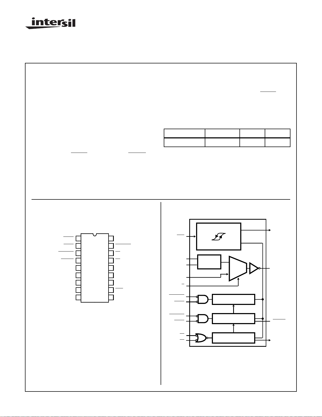
Pinout
82C284/883
(CERDIP)
TOP VIEW
1
ARDY
SRDY
SRDYEN
READY
EFI
F/C
X1
X2
GND
2
3
4
5
6
7
8
9
18
17
16
15
14
13
12
11
10
VCC
ARDYEN
S1
S0
NC
PCLK
RESET
RES
CLK
Description
The Intersil 82C284/883 is a clock generator/driver which
provides clock signals for 80C286 processors and support
components. It also contains logic to supply
READY to the
CPU from either asynchronous or synchronous sources and
synchronous RESET from an asynchronous input with hysteresis.
Ordering Information
PART NUMBER TEMP. RANGE PACKAGE PKG. NO.
MD82C284-12/883 -55oC to +125oC CERDIP F18.3
Functional Diagram
RES
X1
X2
EFI
F/
ARDYEN
ARDY
RESET
SYNCHRONIZER
XTAL
OSC
MUX
C
SYNCHRONIZER
RESET
CLK
SRDYEN
SRDY
S1
S0
CAUTION: These devices are sensitive to electrostatic discharge; follow proper IC Handling Procedures.
http://www.intersil.com or 407-727-9207
MULTIBUS™ is a Trademark of Intel Corporation.
| Copyright © Intersil Corporation 1999
1
READY LOGIC
PCLK GENERATOR
READY
PCLK
File Number 2968.1

82C284/883
Absolute Maximum Ratings Thermal Information
Supply Voltage . . . . . . . . . . . . . . . . . . . . . . . . . . . . . . . . . . . . .+8.0V
Input, Output or I/O Voltage Applied. . . . . GND -0.1V to VCC +1.0V
ESD Classification . . . . . . . . . . . . . . . . . . . . . . . . . . . . . . . . Class 2
CAUTION: Stresses above those listed in the “Absolute Maximum Ratings” may cause permanent damage to the device. This is a stress only rating and operation of the device at these or any other conditions above those indicated in the operation section of this specification is not implied.
Operating Conditions
Operating Temperature Range. . . . . . . . . . . . . . . .-55oC to +125oC
Operating Supply Voltage. . . . . . . . . . . . . . . . . . . . . +4.5V to +5.5V
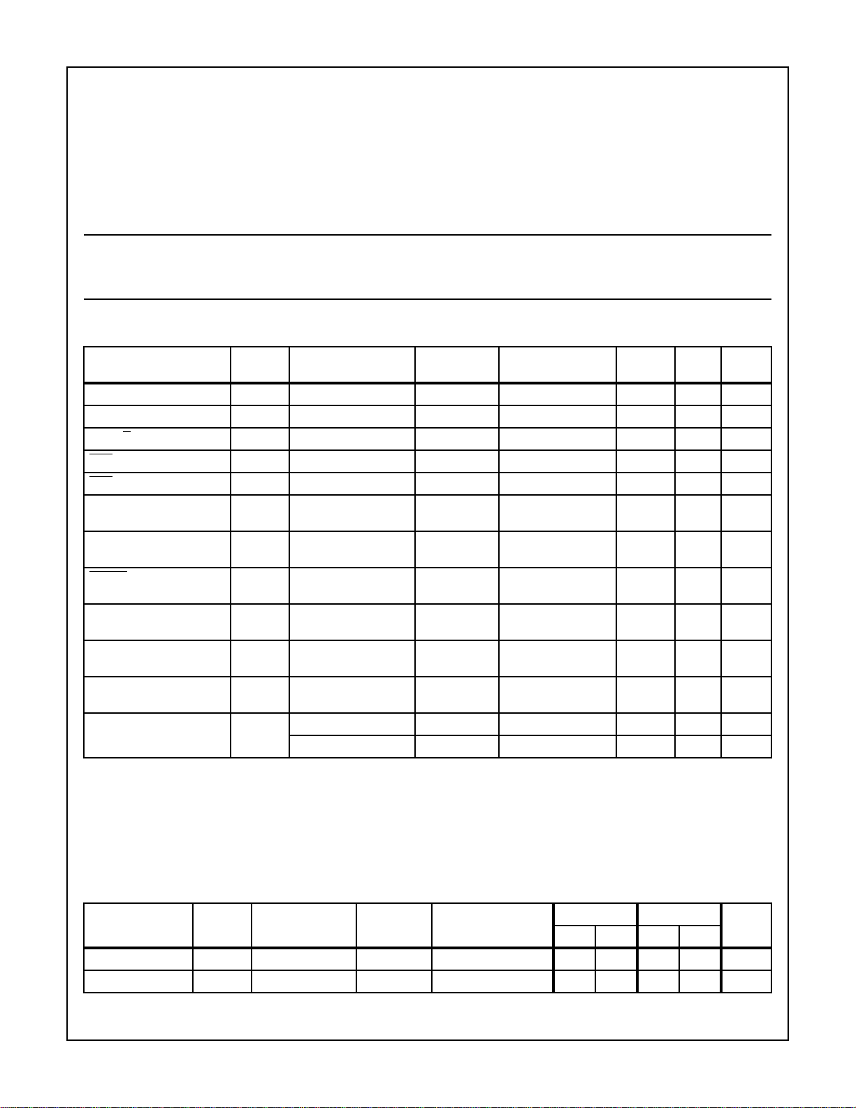
TABLE 1. 82C284/883 D.C. ELECTRICAL PERFORMANCE SPECIFICATIONS
Device Guaranteed and 100% Tested.
PARAMETER SYMBOL CONDITIONS
Input LOW Voltage VIL VCC = 4.5V 1, 2, 3 -55oC ≤ TA≤ +125oC - 0.8 V
Input HIGH Voltage VIH VCC = 5.5V 1, 2, 3 -55oC ≤ TA≤ +125oC 2.2 - V
EFI, F/C Input High Voltage VIHC VCC = 5.5V 1, 2, 3 -55oC ≤ TA≤ +125oC 3.2 - V
RES HIGH Voltage VIHR VCC = 5.5V 1, 2, 3 -55oC ≤ TA≤ +125oC VCC -0.8 - V
RES Input Hysteresis VHYS VCC = 5.5V 1, 2, 3 -55oC ≤ TA≤ +125oC 0.5 - V
RESET, PCLK Output
LOW Voltage
RESET, PCLK Output
Voltage
READY Output LOW
Voltage
CLK Output LOW Voltage VOLC IOL = 5mA,
CLK Output HIGH Voltage VOHC IOH = -5mA,
Input Leakage Current II VIN = GND or VCC,
Active Power Supply
Current
NOTES:
1. ICCOP measured at 10MHz for the 82C284-10/883 and at 12.5MHz for the 82C284-12/883. VIN = GND or VCC, VCC = 5.5V, outputs
unloaded.
2. Interchanging of force and sense conditions is permitted.
VOL IOL = 5mA,
VCC = 4.5V, Note 2
VOH IOH = -1mA,
VCC = 4.5V, Note 2
VOLR IOH = 10mA,
VCC = 4.55V, Note 2
VCC = 4.5V, Note 2
VCC = 4.5V, Note 2
VCC = 5.5V
ICCOP 82C284-10/883, Note 1 1, 2, 3 -55oC ≤ TA≤ +125oC - 48 mA
82C284-12/883, Note 1 1, 2, 3 -55oC ≤ TA≤ +125oC - 60 mA
Thermal Resistance θJA (oC/W) θJC (oC/W)
CERDIP Package . . . . . . . . . . . . . . 80 20
Gate Count . . . . . . . . . . . . . . . . . . . . . . . . . . . . . . . . . . . .200 Gates
Storage Temperature Range. . . . . . . . . . . . . . . . . .-65oC to +150oC
Junction Temperature . . . . . . . . . . . . . . . . . . . . . . . . . . . . . .+175oC
Lead Temperature (Soldering 10s) . . . . . . . . . . . . . . . . . . . .+300oC
EFI Rise Time (From 0.8V to 3.2V). . . . . . . . . . . . . . . . . . 8ns (Max)
EFI Fall Time (From 3.2V to 0.8V). . . . . . . . . . . . . . . . . . . 8ns (Max)
GROUP A
SUBGROUPS TEMPERATURE MIN MAX UNITS
1, 2, 3 -55oC ≤ TA≤ +125oC - 0.4 V
1, 2, 3 -55oC ≤ TA≤ +125oC VCC -0.4 - V
1, 2, 3 -55oC ≤ TA≤ +125oC - 0.4 V
1, 2, 3 -55oC ≤ TA≤ +125oC - 0.4 V
1, 2, 3 -55oC ≤ TA≤ +125oC VCC -0.4 - V
1, 2, 3 -55oC ≤ TA≤ +125oC -10 10 µA
TABLE 2. 82C284/883 A.C. ELECTRICAL PERFORMANCE SPECIFICATIONS
Device Guaranteed and 100% Tested. A.C. timings are referenced to 0.8V and 2.0V points of the signals as illustrated in datasheet waveforms, unless otherwise specified.
(NOTE 1)
PARAMETER SYMBOL
EFI LOW Time t1 At VCC/2, Note 8 9, 10, 11 -55oC ≤ TA≤ +125oC 20 - 16 - ns
EFI HIGH Time t2 At VCC/2, Note 8 9, 10, 11 -55oC ≤ TA≤ +125oC 20 - 20 - ns
CONDITIONS
GROUP A
SUBGROUP TEMPERATURE
10MHz 12MHz
UNITSMIN MAX MIN MAX
2

82C284/883
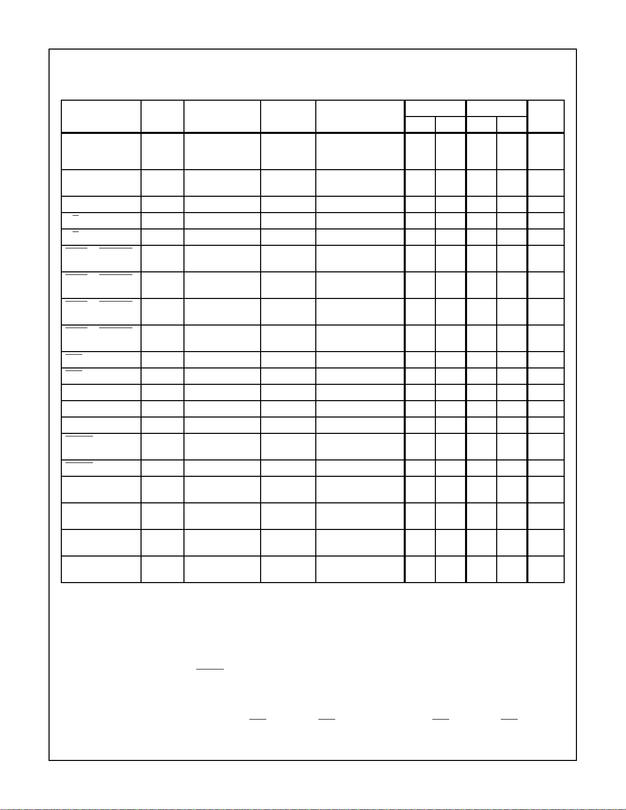
TABLE 2. 82C284/883 A.C. ELECTRICAL PERFORMANCE SPECIFICATIONS (Continued)
Device Guaranteed and 100% Tested. A.C. timings are referenced to 0.8V and 2.0V points of the signals as illustrated in datasheet waveforms, unless otherwise specified. (Continued)
(NOTE 1)
PARAMETER SYMBOL
Status Setup Time
for Status Going
Active
Status Setup Time
for Going Inactive
Status Hold Time t6 9, 10, 11 -55oC ≤ TA≤ +125oC1 - 1 - ns
F/C Setup Time t7 9, 10, 11 -55oC ≤ TA≤ +125oC 15 - 15 - ns
F/C Hold Time t8 9, 10, 11 -55oC ≤ TA≤ +125oC 15 - 15 - ns
SRDY or SRDYEN
Setup Time
SRDY or SRDYEN
Hold Time
ARDY or ARDYEN
Setup Time
ARDY or ARDYEN
Hold Time
RES Setup Time t13 Notes 3, 7 9, 10, 11 -55oC ≤ TA≤ +125oC 20 - 18 - ns
RES Hold Time t14 Notes 3, 7 9, 10, 11 -55oC ≤ TA≤ +125oC10 - 8 - ns
CLK Period t16 9, 10, 11 -55oC ≤ TA≤ +125oC 50 - 40 - ns
CLK LOW Period t17 Notes 2, 6 9, 10, 11 -55oC ≤ TA≤ +125oC 12 - 11 - ns
CLK HIGH Time t18 Notes 2, 6 9, 10, 11 -55oC ≤ TA≤ +125oC 16 - 13 - ns
READY Inactive
Delay
READY Active Delay t22 At 0.8V, Note 4 9, 10, 11 -55oC ≤ TA≤ +125oC - 24 - 18 ns
PCLK Delay t23 CL = 75pF,
RESET Delay t24 CL = 75pF,
PCLK LOW Time t25 CL = 75pF, Note 5 9, 10, 11 -55oC ≤ TA≤ +125oC t16-
PCLK HIGH Time t26 CL = 75pF, Note 5 9, 10, 11 -55oC ≤ TA≤ +125oC t16-
NOTES:
1. VCC = 4.5V and 5.5V unless otherwise specified. CLK loading: CL = 100pF.
2. With the internal crystal oscillator using recommended crystal and capacitive loading; or with the EFI input meeting specifications t1 and t2.
The recommended crystal loading for CLK frequencies of 8MHz to 20MHz are 25pF from pin X1 to GND, and 15pF from pin X2 to GND; for
CLK frequencies from 20MHz to 25MHz the recommended loading is 15pF from pin X1 to GND, and 15pF from X2 to GND. These recommended values are ±5pF and include all stray capacitance. Decouple VCC and GND as close to the 80C284/883 as possible.
3. This is an asychronous input. This specification is given for testing purposes only, to assure recognition at a specific CLK edge.
4. The pull-up resistor value for the READY pin is 620Ω with the rated 150pF load.
5. t16 refers to any allowable CLK period.
6. When using a crystal with the recommended capacitive loading, CLK output HIGH and LOW times are guaranteed to meet 80C286 requirements.
7. Measured from 1.0V on the CLK to 0.8V on the RES waveform for RES active, and to 4.2V on the RES waveform for RES inactive.
8. Input test waveform characteristics: VIL= 0.0V, VIH = 4.5V.
t5A 9, 10, 11 -55oC ≤ TA≤ +125oC 20 - 18 - ns
t5B 9, 10, 11 -55oC ≤ TA≤ +125oC 20 - 16 - ns
t9 9, 10, 11 -55oC ≤ TA≤ +125oC 15 - 15 - ns
t10 9, 10, 11 -55oC ≤ TA≤ +125oC2 - 2 - ns
t11 Note 3 9, 10, 11 -55oC ≤ TA≤ +125oC5 - 5 - ns
t12 Note 3 9, 10, 11 -55oC ≤ TA≤ +125oC 30 - 25 - ns
t21 At 0.8V, Note 4,
CONDITIONS
Test Condition 2
Test Condition 1
Test Condition 3
GROUP A
SUBGROUP TEMPERATURE
9, 10, 11 -55oC ≤ TA≤ +125oC5 - 5 - ns
9, 10, 11 -55oC ≤ TA≤ +125oC - 20 - 16 ns
9, 10, 11 -55oC ≤ TA≤ +125oC - 27 - 26 ns
10MHz 12MHz
- t16-
10
10
10
- t1610
UNITSMIN MAX MIN MAX
-ns
-ns
3
 Loading...