March 1997
80C286/883
High Performance Microprocessor with Memory
Management and Protection
Features
• This Circuit is Processed in Accordance to MIL-STD883 and is Fully Conformant Under the Provisions of
Paragraph 1.2.1.
• Compatible with NMOS 80286/883
• Static CMOS Design for Low Power Operation
- ICCSB = 5mA Maximum
- ICCOP = 185mA Maximum (80C286-10/883)
- ICCOP = 220mA Maximum (80C286-12/883)
• Large Address Space
- 16 Megabytes Physical
- 1 Gigabyte Virtual per Task
• Integrated Memory Management, Four-Level Memory
Protection and Support for Virtual Memory and
Operating Systems
• Two 80C86 Upward Compatible Operating Modes
- 80C286/883 Real Address Mode
- Protected Virtual Address Mode
• Compatible with 80287 Numeric Data Co-Processor
Description
The Intersil 80C286/883 is a static CMOS version of the
NMOS 80286 microprocessor. The 80C286/883 is an
advanced, high-performance microprocessor with specially
optimized capabilities for multiple user and multi-tasking systems. The 80C286/883 has built-in memory protection that
supports operating system and task isolation as well as program and data privacy within tasks. The 80C286/883
includes memory management capabilities that map 230
(one gigabyte) of virtual address space per task into 2
bytes (16 megabytes) of physical memory.
The 80C286/883 is upwardly compatible with 80C86 and
80C88 software (the 80C286/883 instruction set is a superset of the 80C86/80C88 instruction set). Using the 80C286/
883 real address mode, the 80C286/883 is object code compatible with existing 80C86 and 80C88 software . In protected
virtual address mode, the 80C286/883 is source code compatible with 80C86 and 80C88 software but may require
upgrading to use virtual address as supported by the
80C286/883’s integrated memory management and protection mechanism. Both modes operate at full 80C286/883
performance and execute a superset of the 80C86 and
80C88 instructions.
The 80C286/883 provides special operations to support the
efficient implementation and execution of operating systems.
For example, one instruction can end execution of one task,
save its state, switch to a new task, load its state, and start
execution of the new task. The segment-not-present exception and restartable instructions.
24
Ordering Information
PACKAGE TEMP. RANGE 10MHz 12.5MHz 16MHz 20MHz 25MHz PKG. NO.
68 Pin PGA 0oC to +70oC - CG80C286-12 CG80C286-16 CG80C286-20 - G68.B
-40oC to +85oC IG80C286-10 IG80C286-12 - - - G68.B
-55oC to +125oC MG80C286-10/883 MG80C286-12/883 - - - G68.B
5962-9067801MXC 5962-9067802MXC - - - G68.B
CAUTION: These devices are sensitive to electrostatic discharge; follow proper IC Handling Procedures.
http://www.intersil.com or 407-727-9207
| Copyright © Intersil Corporation 1999
3-128
File Number 2948.1

80C286/883
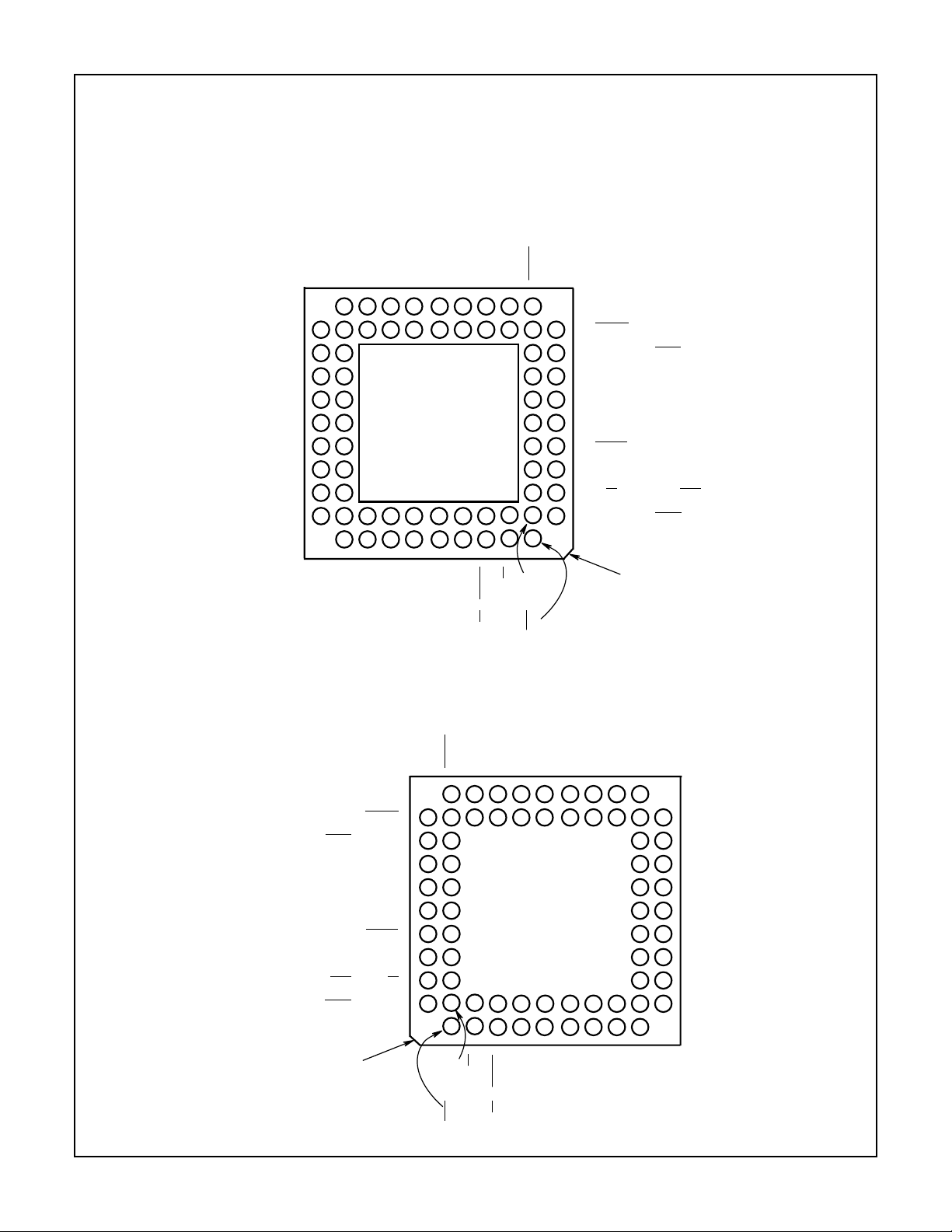
Pinout
68 LEAD PGA, COMPONENT PAD VIEW
As viewed from underside of the component when mounted on the board.
SS
D8
V
D1
D0
35 37
D0
V
A11
A13
A0
A1
A2
CLK
CC
RESET
A3
A4
A5
A6
A7
A8
A9
A10
A12
36
38 40
34
33
32
31
30
29
28
27
26
25
24
23
22
2120
1918
1517
A15
A12
A16
A14
As viewed from the component side of the P.C. board.
D11
D10
D9
D4
D3
D2
39 41
1416
A17
A18
42 44
1113
A19
A20
43 45
10
A21
SS
V
P.C. BOARD VIEW
D12
D5
46 48
A22
A23
D13
D6
47 49
6812
579
PEACK
S0
D15
D14
ERROR
D7
51
50
55
57
59
61
63
65
67
2
4
13
S1
NC
NC
BHE
ERROR
5253
NC
54
INTR
56
NMI
58
PEREQ
60
READY
62
HLDA
64
66
M/
IO
68
NC
NC
BUSY
NC
NC
V
SS
V
CC
HOLD
COD/INTA
LOCK
PIN 1 INDICATOR
NC
BUSY
NC
NC
V
SS
V
CC
HOLD
COD/
INTA
LOCK
PIN 1 INDICATOR
ERROR
NC
INTR
NMI
PEREQ
READY
HLDA
M/
NC
D1
3840
15 17
A15
A16
SS
V
D0
3537
36
33
31
29
27
25
23
21 20
19 18
A12
A14
D0
A1
CLK
RESET
A4
A6
A8
A10
A12
A0
A2
V
A3
A5
A7
A9
A11
A13
CC
34
32
30
28
26
24
22
D15
D14
D13
D12
D11
D10D9D8
ERROR
D7
D6
D5
D4
D3
D2
A21
SS
V
4244
11 13
A19
A20
3941
14 16
A17
A18
4749
51
50
52 53
54
55
56
57
58
59
60
61
62
63
64
65
66
68
67
2
4
13
S1
NC
NC
BHE
IO
4345
4648
10
68 12
579
A22
PEACK
S0
A23
3-129

80C286/883
Absolute Maximum Ratings Thermal Information
Supply Voltage . . . . . . . . . . . . . . . . . . . . . . . . . . . . . . . . . . . . .+8.0V
Input, Output or I/O Voltage Applied. . . . . .GND -1.0V to VCC+1.0V
Storage Temperature Range . . . . . . . . . . . . . . . . . -65oC to +150oC
Junction Temperature . . . . . . . . . . . . . . . . . . . . . . . . . . . . . . +175oC
Lead Temperature (Soldering 10s). . . . . . . . . . . . . . . . . . . . +300oC
ESD Classification . . . . . . . . . . . . . . . . . . . . . . . . . . . . . . . . Class 1
CAUTION: Stresses above those listed in “Absolute Maximum Ratings” may cause permanent damage to the device. This is a stress only rating and operation
of the device at these or any other conditions above those indicated in the operational sections of this specification is not implied.
NOTE:
1. θJA is measured with the component mounted on an evaluation PC board in free air.
Operating Conditions
Operating Voltage Range . . . . . . . . . . . . . . . . . . . . . +4.5V to +5.5V
Operating Temperature Range . . . . . . . . . . . . . . . . -55oC to +125oC
System Clock (CLK) RISE Time (From 1.0V to 3.6V . . . . 8ns (Max)
System Clock (CLK) FALL Time (from 3.6V to 1.0V) . . . . 8ns (Max)
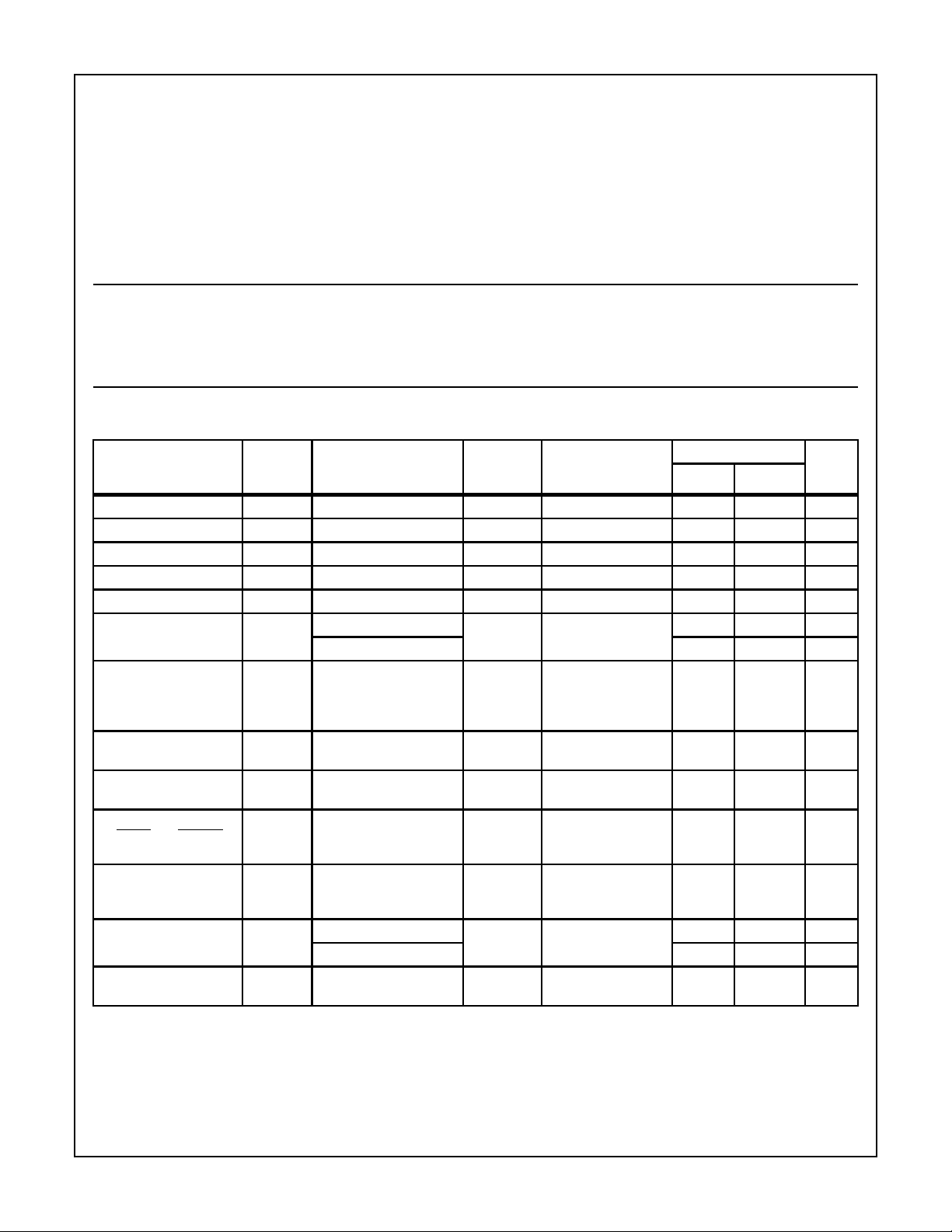
TABLE 1. 80C286/883 D.C. ELECTRICAL PERFORMANCE SPECIFICATIONS
Device Guaranteed and 100% Tested
PARAMETER SYMBOL CONDITIONS
Input LOW Voltage V
Input HIGH Voltage V
CLK Input LOW Voltage V
CLK Input HIGH Voltage V
Output LOW Voltage V
Output HIGH Voltage V
Input Leakage Current I
Input Sustaining Current
LOW
Input Sustaining Current
I
BHL
I
BHH
HIGH
Input Sustaining Current
BUSY and ERROR
on
I
Pins
Output Leakage Current I
Active Power Supply
I
CCOP
Current
Standby Power
I
CCSB
Supply Current
NOTES:
2. I
should be measured after lowering VIN to GND and then raising to 1.0V on the following pins: 36-51, 66, 67.
BHL
3. I
should be measured after raising VIN to VCC and then lowering to 3.0V on the following pins: 4-6, 36-51, 66-68.
BHH
4. I
5. I
should be tested with the clock stopped in phase two of the processor clock cycle. VIN = VCC or GND, VCC = 5.5V, outputs unloaded.
CCSB
measured at 10MHz for the 80C286-10/883 and 12.5MHz for the 80C286-12/883. VIN = 2.4V or 0.4V, VCC = 5.5V, outputsunloaded.
CCOP
6. ISH should be measured after raising VIN to VCC and then lowering to 0V on pins 53 and 54.
VCC = 4.5V 1, 2, 3 -55oC ≤ TA≤ +125oC -0.5 0.8 V
IL
VCC = 5.5V 1, 2, 3 -55oC ≤ TA≤ +125oC 2.0 VCC +0.5 V
IH
VCC = 4.5V 1, 2, 3 -55oC ≤ TA≤ +125oC -0.5 1.0 V
ILC
VCC = 5.5V 1, 2, 3 -55oC ≤ TA≤ +125oC 3.6 VCC +0.5 V
IHC
IOL = 2.0mA, VCC = 4.5V 1, 2, 3 -55oC ≤ TA≤ +125oC - 0.4 V
OL
OHIOH
I
= -2.0mA, VCC = 4.5V 1, 2, 3 -55oC ≤ TA≤ +125oC 3.0 - V
= -100µA, VCC = 4.5V VCC -0.4 - V
I
OH
VIN = GND or VCC,
VCC = 5.5V,
Pins 29, 31, 57, 59, 61,
63-64
VCC = 4.5V and 5.5V,
VIN = 1.0V, Note 1
VCC = 4.5V and 5.5V,
VIN = 3.0V, Note 2
VCC = 4.5V and 5.5V
SH
VIN = GND, Note 5
VO = GND or V
O
CC
VCC = 5.5V,
Pins 1, 7-8, 10-28, 32-34
80C286-10/883, Note 4 1, 2, 3 -55oC ≤ TA≤ +125oC - 185 mA
80C286-12/883, Note 4 - 220 mA
VCC = 5.5V, Note 3 1, 2, 3 -55oC ≤ TA≤ +125oC- 5 mA
Thermal Resistance (Typical) θ
JA
θ
PGA Package . . . . . . . . . . . . . . . . . . . . . 35oC/W 6oC/W
Gate Count . . . . . . . . . . . . . . . . . . . . . . . . . . . . . . . . . 22,500 Gates
Input RISE and FALL Time (From 0.8V to 2.0V
80C286-10/883 . . . . . . . . . . . . . . . . . . . . . . . . . . . . . . 10ns (Max)
80C286-12/883 . . . . . . . . . . . . . . . . . . . . . . . . . . . . . . . 8ns (Max)
GROUP A
LIMITS
SUB-
GROUPS TEMPERATURE
UNITS MIN MAX
1, 2, 3 -55oC ≤ TA≤ +125oC -10 10 µA
1, 2, 3 -55oC ≤ TA≤ +125oC 38 200 µA
1, 2, 3 -55oC ≤ TA≤ +125oC -50 -400 µA
1, 2, 3 -55oC ≤ TA≤ +125oC -30 -500 µA
1, 2, 3 -55oC ≤ TA≤ +125oC -10 10 µA
JC
3-130

80C286/883
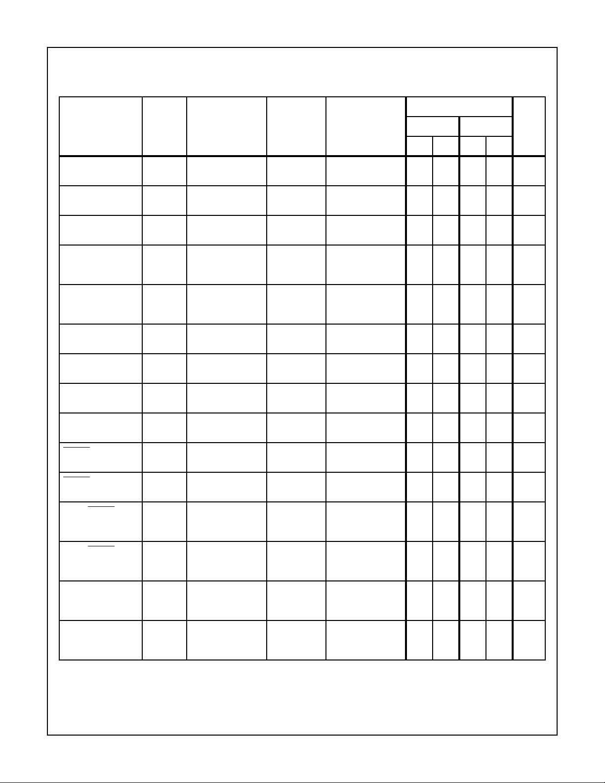
TABLE 2. 80C286/883 AC ELECTRICAL PERFORMANCE SPECIFICATIONS
AC Timings are Referenced to 0.8V and 2.0V Points of the Signals as Illustrated in Datasheet Waveforms, Unless Otherwise Noted. Device
Guaranteed and 100% Tested.
80C286/883
10MHz 12.5MHz
GROUP A
PARAMETER SYMBOL CONDITIONS
SUBGROUPS TEMPERATURE
MIN MAX MIN MAX
UNITS
System Clock
(CLK) Period
System Clock
(CLK) Low Time
System Clock (CLK)
High Time
Asynchronous Inputs
SETUP Time
(Note 1)
Asynchronous Inputs
HOLD Time
(Note 1)
RESET SETUP Time 6 VCC = 4.5V
RESET HOLD Time 7 VCC = 4.5V
Read Data
SETUP Time
Read Data
HOLD Time
READY SETUP Time 10 VCC = 4.5V
1VCC = 4.5V and 5.5V 9, 10, 11 -55oC ≤TA≤ +125oC 50 - 40 - ns
2VCC = 4.5V and 5.5V
at 1.0V
3VCC = 4.5V and 5.5V
at 3.6V
4VCC = 4.5V
and 5.5V
5VCC = 4.5V
and 5.5V
and 5.5V
and 5.5V
8VCC = 4.5V
and 5.5V
9VCC = 4.5V
and 5.5V
and 5.5V
9, 10, 11 -55oC ≤TA≤ +125oC 12 - 11 - ns
9, 10, 11 -55oC ≤TA≤ +125oC 16 - 13 - ns
9, 10, 11 -55oC ≤TA≤ +125oC 20 - 15 - ns
9, 10, 11 -55oC ≤ TA≤ +125oC 20 - 15 - ns
9, 10, 11 -55oC ≤ TA≤ +125oC 19 - 10 - ns
9, 10, 11 -55oC ≤ TA≤ +125oC0 - 0 - ns
9, 10, 11 -55oC ≤ TA≤ +125oC8 - 5 - ns
9, 10, 11 -55oC ≤ TA≤ +125oC4 - 4 - ns
9, 10, 11 -55oC ≤ TA≤ +125oC 26 - 20 - ns
READY HOLD Time 11 VCC = 4.5V
and 5.5V
Status/PEACK Active
Delay, (Note 4)
Status/PEACK
Inactive Delay
(Note 3)
Address Valid
Delay (Note 2)
Write Data
Valid Delay, (Note 2)
12A VCC = 4.5V and
5.5V, CL = 100pF
IL = |2mA|
12B VCC = 4.5V and
5.5V, CL = 100pF
IL = |2mA|
13 VCC = 4.5V and
5.5V, CL = 100pF
IL = |2mA|
14 VCC = 4.5V and
5.5V, CL = 100pF
IL = |2mA|
9, 10, 11 -55oC ≤TA≤ +125oC 25 - 20 - ns
9, 10, 11 -55oC ≤ TA≤ +125oC 1 22 1 21 ns
9, 10, 11 -55oC ≤ TA≤ +125oC 1 30 1 24 ns
9, 10, 11 -55oC ≤ TA≤ +125oC 1 35 1 32 ns
9, 10, 11 -55oC ≤ TA≤ +125oC 0 40 0 31 ns
3-131
 Loading...