

Page 1
®
www.BDTIC.com/Intersil
5962-0721201QXC
Data Sheet November 1, 2007
Video Distribution Amplifier
The 5962-0721201QXC is a fully DSCC SMD compliant
parts and the SMD data sheets is available on the DSCC
website (http://www.dscc.dla.mil/
programs/specfind/default.asp). The 5962-0721201QXC is
electrically equivalent to the EL8108. Reference equivalent
“EL8108” data sheet for additional information. The 59620721201QXC is a dual current feedback operational
amplifier designed for video distribution solutions. This
device features a high drive capability of 450mA while
consuming 13mA of supply current per amplifier and
operating from a single 5V to 12V supply.
The 5962-0721201QXC is available in the industry standard
10 Ld Flatpack. The 5962-0721201QXC is ideal for driving
multiple video loads while maintaining linearity.
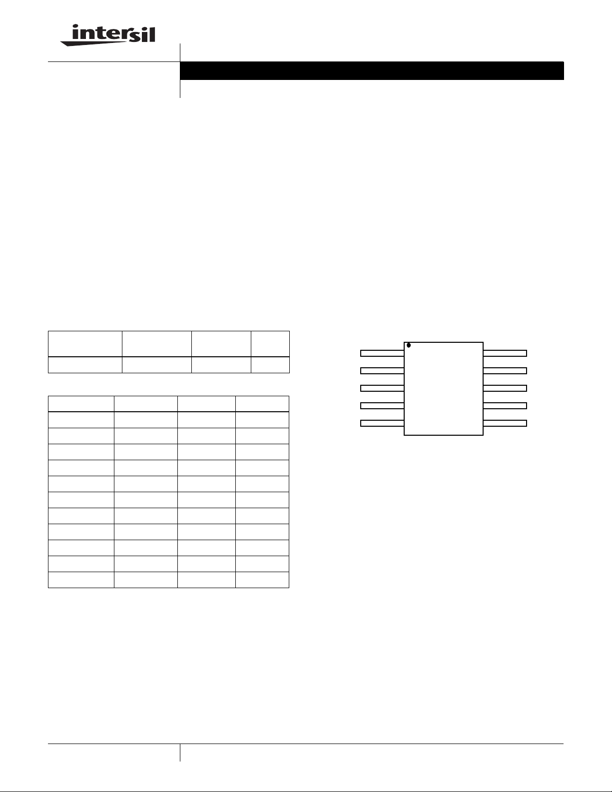
Ordering Information
PKG.
PART NUMBER PART MARKING PACKAGE
5962-0721201QXC 07212 01QHC 10 Ld Flat Pack K10.A
TABLE 1.
150Ω 150Ω DIFF GAIN DIFF PHASE
1 0 0.03 0.01
1 1 0.03 0.01
2 1 0.05 0.02
2 2 0.06 0.03
3 2 0.08 0.03
3 3 0.11 0.03
2 0 0.04 0.01
3 0 0.05 0.02
4 0 0.07 0.02
5 0 0.08 0.03
6 0 0.10 0.03
DWG. #
FN6558.1
Features
• Drives up to 450mA from a +12V supply
•20V
differential output drive into 100Ω
P-P
• -85dBc typical driver output distortion at full output at
150kHz
• -70dBc typical driver output distortion at 3.75MHz
• Low quiescent current of 13mA per amplifier
• 300MHz bandwidth
Applications
• Video distribution amplifiers
Pinout
5962-0721201QXC
(10 LD FLATPACK)
TOP VIEW
1
2
3
4
5
OUTA
INA-
INA+
GND
INB+
NC
NC
VS+
OUTB
INB-
10
9
8
7
6
1
CAUTION: These devices are sensitive to electrostatic discharge; follow proper IC Handling Procedures.
1-888-INTERSIL or 1-888-468-3774
| Intersil (and design) is a registered trademark of Intersil Americas Inc.
All other trademarks mentioned are the property of their respective owners.
Copyright Intersil Americas Inc. 2007. All Rights Reserved
Page 2
5962-0721201QHC
www.BDTIC.com/Intersil
Absolute Maximum Ratings (T
VS+ Voltage to Ground . . . . . . . . . . . . . . . . . . . . . . -0.3V to +13.2V
V
+ Voltage . . . . . . . . . . . . . . . . . . . . . . . . . . . . . . . . . GND to VS+
IN
Current into any Input . . . . . . . . . . . . . . . . . . . . . . . . . . . . . . . . 8mA
Continuous Output Current . . . . . . . . . . . . . . . . . . . . . . . . . . . 60mA
= +25°C) Thermal Information
A
Thermal Resistance (Typical) θ
10 Lead Flatpack . . . . . . . . . . . . . . . . . . . . . . . . . . . 177
Ambient Operating Temperature Range . . . . . . . . .-55°C to +125°C
Storage Temperature Range . . . . . . . . . . . . . . . . . .-60°C to +150°C
(°C/W)
JA
Operating Junction Temperature . . . . . . . . . . . . . . . . . . . . . .+150°C
CAUTION: Do not operate at or near the maximum ratings listed for extended periods of time. Exposure to such conditions may adversely impact product reliability and
result in failures not covered by warranty.
IMPORTANT NOTE: All parameters having Min/Max specifications are guaranteed. Typical values are for information purposes only. Unless otherwise noted, all tests
are at the specified temperature and are pulsed tests, therefore: TJ = TC = T
Electrical Specifications V
= 12V, RF = 750Ω, RL = 100Ω connected to mid supply, T
S
A
= +25°C, unless otherwise specified.
A
PARAMETER DESCRIPTION CONDITIONS MIN TYP MAX UNIT
AC PERFORMANCE
BW -3dB Bandwidth R
HD Total Harmonic Distortion, Differential f = 200kHz, V
SR Slew Rate, Single-ended V
= 500Ω, AV = +2 200 MHz
F
= 500Ω, AV = +4 150 MHz
R
F
= 16V
O
f = 4MHz, VO = 2V
f = 8MHz, V
f = 16MHz, V
OUT
= 2V
O
= 2V
O
from -3V to +3V 800 V/µs
, RL = 50Ω -83 dBc
P-P
, RL = 100Ω -70 dBc
P-P
, RL = 100Ω -60 dBc
P-P
, RL = 100Ω -50 dBc
P-P
INPUT CHARACTERISTICS
e
N
i
N
Input Noise Voltage 6nV
-Input Noise Current 13 pA/√Hz
Hz
√
OUTPUT CHARACTERISTICS
I
OUT
Output Current RL = 0Ω 450 mA
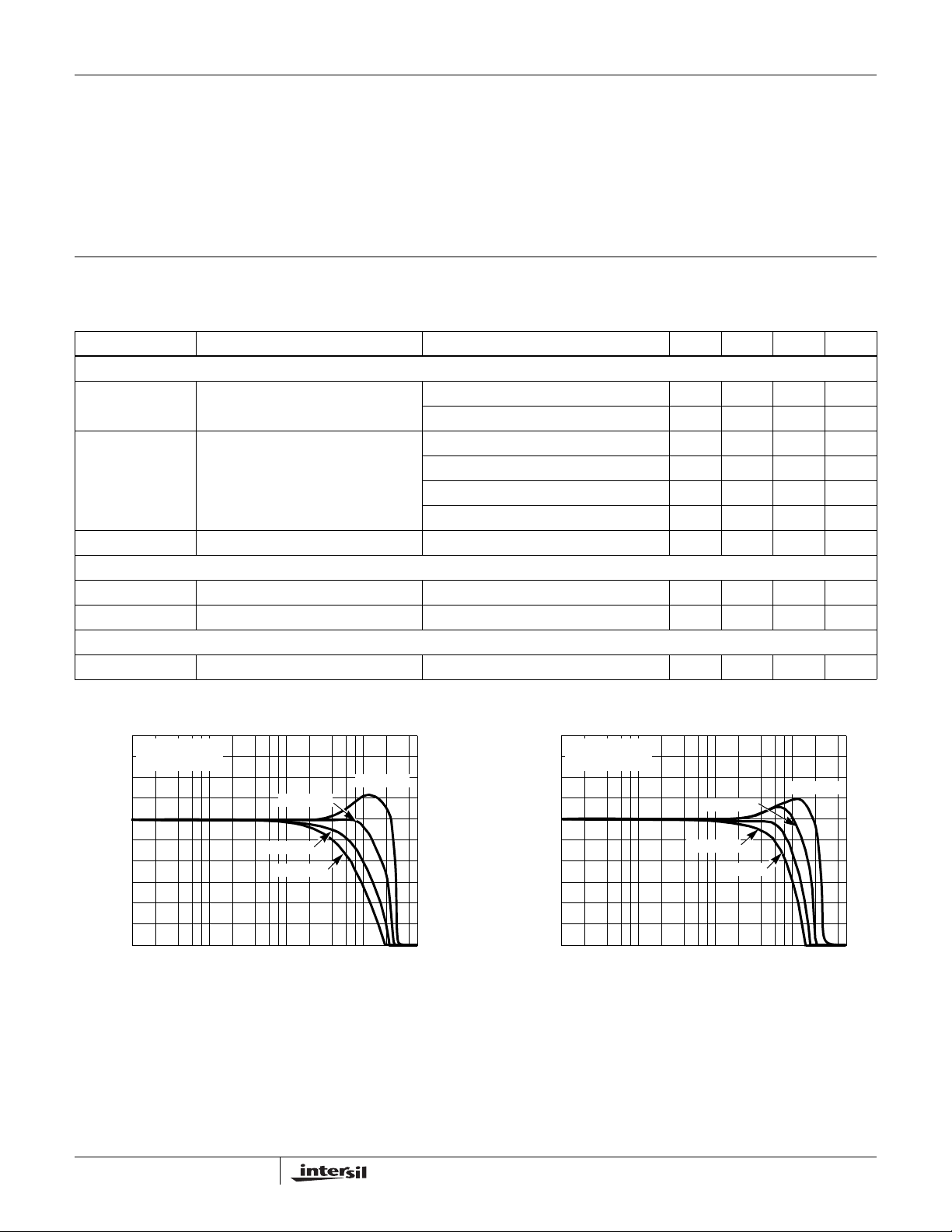
Typical Performance Curves
22
VS = ±6V, AV = 5
20
R
= 100Ω DIFF
L
18
16
14
12
10
GAIN (dB)
8
6
4
2
100k
1M
FREQUENCY (Hz)
RF = 500Ω
RF = 750Ω
RF = 1kΩ
10M 100M
FIGURE 1. DIFFERENTIAL FREQUENCY RESPONSE WITH
VARIOUS R
(FULL POWER MODE)
F
RF = 243Ω
500M
22
VS = ±6V, AV = 5
20
R
= 100Ω DIFF
L
18
16
14
12
10
GAIN (dB)
8
6
4
2
100k
1M
RF = 500Ω
RF = 750Ω
RF = 1kΩ
10M 100M
FREQUENCY (Hz)
RF = 243Ω
500M
FIGURE 2. DIFFERENTIAL FREQUENCY RESPONSE WITH
VARIOUS RF (3/4 POWER MODE)
2
FN6558.1
November 1, 2007
Page 3
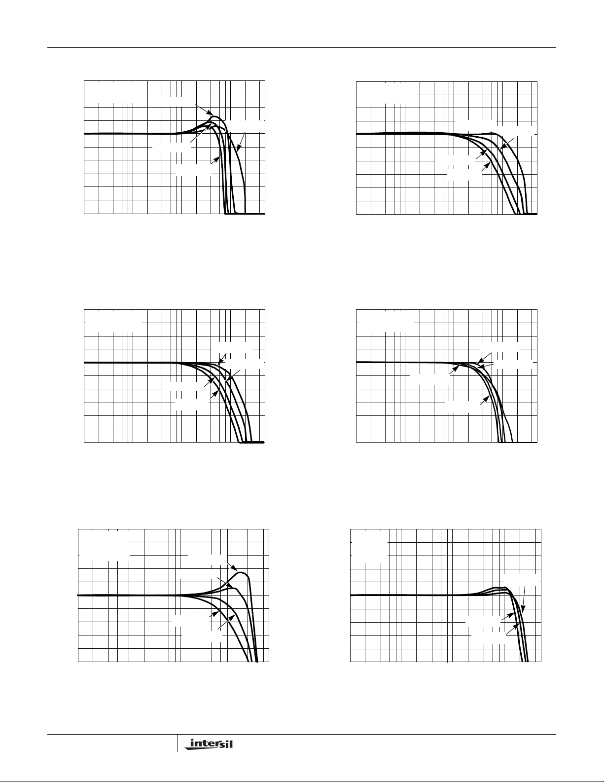
Typical Performance Curves (Continued)
www.BDTIC.com/Intersil
22
VS = ±6V, AV = 5
20
R
= 100Ω DIFF
L
18
16
14
12
10
GAIN (dB)
8
6
4
2
100k
1M
FIGURE 3. DIFFERENTIAL FREQUENCY RESPONSE WITH
VARIOUS R
RF = 500Ω
RF = 750Ω
RF = 1kΩ
10M 100M
FREQUENCY (Hz)
(1/2 POWER MODE)
F
RF = 243Ω
5962-0721201QHC
28
26
24
22
20
18
16
GAIN (dB)
14
12
10
500M
FIGURE 4. DIFFERENTIAL FREQUENCY RESPONSE WITH
VS = ±6V, AV = 10
R
= 100Ω DIFF
L
8
100k
VARIOUS R
RF = 750Ω
RF = 1kΩ
1M
F
10M 100M
FREQUENCY (Hz)
(FULL POWER MODE)
RF = 243Ω
RF = 500Ω
500M
28
VS = ±6V, AV = 10
26
R
= 100Ω DIFF
L
24
22
20
18
16
GAIN (dB)
14
12
10
8
100k
1M
RF = 750Ω
RF = 1kΩ
10M 100M
FREQUENCY (Hz)
RF = 243Ω
RF = 500Ω
500M
FIGURE 5. DIFFERENTIAL FREQUENCY RESPONSE WITH
VARIOUS R
VS = ±6V
14
= 2
A
V
= 100Ω DIFF
R
L
12
10
8
6
4
GAIN (dB)
2
0
-2
(3/4 POWER MODE)
F
RF = 248Ω
RF = 500Ω
RF = 1kΩ
RF = 750Ω
28
VS = ±6V, AV = 10
26
R
= 100Ω DIFF
L
24
22
20
18
16
GAIN (dB)
14
12
10
8
100k
RF = 243Ω
1M
FREQUENCY (Hz)
RF = 1kΩ
10M 100M
RF = 500Ω
RF = 750Ω
500M
FIGURE 6. DIFFERENTIAL FREQUENCY RESPONSE WITH
VARIOUS RF (1/2 POWER MODE)
VS = ±6V
8
A
= 2
V
= 500Ω
R
F
6
4
2
0
-2
-4
NORMALIZED GAIN (dB)
-6
-8
RL = 25Ω
RL = 50Ω
RL = 150Ω
100k 1M 10M 100M 500M
FREQUENCY (Hz)
FIGURE 7. DIFFERENTIAL FREQUENCY RESPONSE WITH
VARIOUS R
F
100k 1M 10M 100M 500M
FIGURE 8. FREQUENCY RESPONSE FOR VARIOUS R
3
FREQUENCY (Hz)
LOAD
FN6558.1
November 1, 2007
Page 4

Typical Performance Curves (Continued)
www.BDTIC.com/Intersil
5962-0721201QHC
-50
VS = ±6V
A
= 5
V
-55
R
= 50Ω DIFF
L
R
= 750
F
-60
-65
-70
HD (dB)
-75
-80
-85
123456789
3rd HD
V
OP-P
2nd HD
(V)
FIGURE 9. DISTORTION AT 2MHz
-40
VS = ±6V
= 5
A
V
-45
= 50Ω DIFF
R
L
R
= 750
F
-50
-55
3rd HD
-50
VS = ±6V
= 5
A
V
-55
= 50Ω DIFF
R
L
= 750
R
F
-60
-65
HD (dB)
-70
-75
-80
123456789
3rd HD
V
OP-P
2nd HD
(V)
FIGURE 10. DISTORTION AT 3MHz
-40
VS = ±6V
= 5
A
V
= 50Ω DIFF
R
L
-45
R
= 750
F
-50
3rd HD
-60
HD (dB)
-65
-70
-75
123456789
V
OP-P
2nd HD
(V)
FIGURE 11. DISTORTION AT 5MHz FIGURE 12. DISTORTION AT 10MHz
-70
VS = ±6V
= 5
A
V
-75
= 750
R
F
= 4V
V
OPP
-80
-85
HD (dB)
-90
-95
-100
50 60 70 80 90 100 110 120 150
3rd HD
2nd HD
R
LOAD
(Ω)
130 140
FIGURE 13. 2nd AND 3rd HARMONIC DIST ORTION vs R
@ 2MHz
LOAD
HD (dB)
-55
(V)
3rd HD
(Ω)
2nd HD
130 140
LOAD
-60
-65
123456789
-60
VS = ±6V
= 5
A
V
-65
= 750
R
F
V
= 4V
OPP
-70
-75
HD (dB)
-80
-85
-90
50 60 70 80 90 100 110 120 150
FIGURE 14. 2nd AND 3rd HARMONIC DIST ORTION vs R
V
2nd HD
R
OP-P
LOAD
@ 3MHz
4
FN6558.1
November 1, 2007
Page 5

Typical Performance Curves (Continued)
www.BDTIC.com/Intersil
5962-0721201QHC
-50
-55
-60
-65
-70
HD (dB)
-75
-80
-85
-90
50 60 70 80 90 100 110 120 150
2nd HD
R
LOAD
3rd HD
(Ω)
VS = ±6V
= 5
A
V
= 750
R
F
V
OPP
130 140
= 4V
FIGURE 15. 2nd AND 3rd HARMONIC DIST ORTION vs R
@ 5MHz
VS = ±6V, AV = 5
22
R
= 50Ω
L
R
= 750Ω
20
F
18
16
14
12
GAIN (dB)
10
8
6
0
100k
1M
FREQUENCY (Hz)
CL = 47pF
CL = 33pF
CL = 0pF
CL = 22pF
10M 100M
FIGURE 17. FREQUENCY RESPONSE WITH VARIOUS C
LOAD
500M
-40
-45
-50
-55
-60
HD (dB)
-65
-70
-75
-80
50 60 70 80 90 100 110 120 150
FIGURE 16. 2nd AND 3rd HARMONIC DIST ORTION vs R
2nd HD
R
LOAD
3rd HD
(Ω)
@ 10MHz
24
VS = ±6V, AV = 5
22
R
= 50Ω
L
R
= 750Ω
20
F
18
16
14
12
GAIN (dB)
10
8
6
4
100k
L
FIGURE 18. FREQUENCY RESPONSE vs VARIOUS CL
1M
FREQUENCY (Hz)
(3/4 POWER MODE)
CL = 47pF
CL = 39pF
CL = 12pF
CL = 0pF
10M 100M
VS = ±6V
= 5
A
V
= 750
R
F
V
OPP
130 140
= 4V
500M
LOAD
24
VS = ±6V, AV = 5
22
R
= 50Ω
L
R
= 750Ω
20
F
18
16
14
12
GAIN (dB)
10
8
6
4
100k
1M
FREQUENCY (Hz)
CL = 12pF
CL = 0pF
10M 100M
CL = 47pF
CL = 37pF
FIGURE 19. FREQUENCY RESPONSE WITH VARIOUS C
(1/2 POWER MODE)
500M
L
-10
-30
-50
-70
-90
CHANNEL SEPARATION (dB)
-110
10k
FIGURE 20. CHANNEL SEPARATION vs FREQUENCY
5
100k
FREQUENCY (Hz)
A B
B A
1M 10M
100M
FN6558.1
November 1, 2007
Page 6

Typical Performance Curves (Continued)
www.BDTIC.com/Intersil
5962-0721201QHC
-10
-30
-50
-70
PSRR (dB)
-90
-110
100k 1M 10M 10M 100M
FREQUENCY (Hz)
PSRR+
PSRR-
200M
10M
3M
300k
100k
30k
10k
MAGNITUDE (Ω)
3k
1k
-110
1k 10k 100k 1M 10M
GAIN
FREQUENCY (Hz)
PHASE
100M
FIGURE 21. PSRR vs FREQUENCY FIGURE 22. TRANSIMPEDANCE (ROL) vs FREQUENCY
1000
0.01
0.001
0.0001
VOLTAGE/CURRENT NOISE (nV/√Hz)(nA/√Hz)
100
10
0.1
EN
1
IN-
IN+
10010
1k 10k 100k 1M 10M
FREQUENCY (Hz)
10
1
OUTPUT IMPEDANCE (Ω)
0.1
10k
VS = ±6V, AV = 1
R
= 750Ω
F
100k
1M 10M
FREQUENCY (Hz)
100M
FIGURE 23. VOLTAGE AND CURRENT NOISE vs FREQUENCY FIGURE 24. OUTPUT IMPEDANCE vs FREQUENCY
200
150
100
50
0
-50
-100
-150
-200
PHASE (°)
150
AV = 5, RF = 750Ω,
130
R
= 100Ω DIFF
LOAD
120
110
FULL POWER MODE
100
90
3/4 POWER MODE
BW (MHz)
80
70
60
50
3.0 3.5 4.0 4.5 5.0 5.5 6.0
1/2 POWER MODE
±VS (V)
0.40
VS = ±6V
0.35
0.30
0.25
0.20
0.15
0.10
DIFFERENTIAL GAIN (%)
0.05
0
1234
FIGURE 25. DIFFERENTIAL BANDWIDTH vs SUPPLY VOL TAGE FIGURE 26. DIFFERENTIAL GAIN
6
FULL POWER MODE
# OF 150Ω LOADS
1/2 POWER MODE
3/4 POWER MODE
FN6558.1
November 1, 2007
Page 7

Typical Performance Curves (Continued)
www.BDTIC.com/Intersil
5962-0721201QHC
0.09
VS = ±6V
0.08
0.07
0.06
0.05
0.04
0.03
DIFFERENTIAL PHASE (%)
1/2 POWER MODE
0.02
0.01
1234
FULL POWER MODE
3/4 POWER MODE
# OF 150Ω LOADS
FIGURE 27. DIFFERENTIAL PHASE FIGURE 28. SUPPLY CURRENT vs SUPPLY VOLTAGE
1
0
IB+
-1
16
14
12
10
8
(mA)
S
I
6
4
2
0
1246
1.8k
1.7k
1.6k
FULL POWER MODE
3/4 POWER MODE
35
(V)
±V
S
1/2 POWER MODE
+IS
-IS
-2
-3
INPUT BIAS CURRENT (µA)
-4
-5
0 25 50 75 100 125 150
TEMPERATURE (°C)
IB-
1.5k
1.4k
SLEW RATE (V/µs)
1.3k
1.2k
-50 -25 0
25 50 75 100 125 150
TEMPERATURE (°C)
FIGURE 29. INPUT BIAS CURRENT vs TEMPERATURE FIGURE 30. SLEW RATE vs TEMPERATURE
5
4
3
2
1
OFFSET VOLTAGE (mV)
0
-1
-50 -25 0
25 50 75 100 125 150
TEMPERATURE (°C)
FIGURE 31. OFFSET VOLTAGE vs TEMPERATURE
3.0
2.5
2.0
1.5
1.0
TRANSIMPEDANCE (MΩ)
0.5
0
-50 -25 0
25 50 75 100 125 150
TEMPERATURE (°C)
FIGURE 32. TRANSIMPEDANCE vs TEMPERATURE
7
FN6558.1
November 1, 2007
Page 8

Typical Performance Curves (Continued)
www.BDTIC.com/Intersil
5962-0721201QHC
5.10
R
= 100Ω
LOAD
VS = ±6V
5.05
5.00
4.95
4.90
4.85
OUTPUT VOLTAGE (±V)
4.80
4.75
-50 -25 0
FIGURE 33. OUTPUT VOLTAGE vs TEMPERATURE
25 50 75 100 125 150
TEMPERATURE (°C)
3
AV = 5
R
F
R
L
2
1
PEAKING (dB)
0
= 750Ω
= 100Ω DIFF
16.0
15.5
15.0
14.5
14.0
13.5
13.0
SUPPLY CURRENT (mA)
12.5
12.0
-50 -25 0
FIGURE 34. SUPPLY CURRENT vs TEMPERATURE
25 50 75 100 125 150
TEMPERATURE (°C)
-1
2.5 3.0 3.5 4.0 4.5 5.0 5.5 6.0
FIGURE 35. DIFFERENTIAL PEAKING vs SUPPLY VOLTAGE
Applications Information
Product Description
The 5962-0721201QXC is a dual current feedback
operational amplifier designed for video distribution solutions.
It is a dual current mode feedback amplifier with low distortion
while drawing moderately low supply current. It is built using
Intersil’s proprietary complimentary bipolar process. Due to
the current feedback architecture, the 5962-0721201QXC
closed-loop 3dB bandwidth is dependent on the value of the
feedback resistor. First the desired bandwidth is selected by
choosing the feedback resistor, R
picking the gain resistor, R
the Typical Performa nce Curves se ctio n show the effect of
varying both R
and RG. The 3dB bandwidth is somewhat
F
dependent on the power supply voltage.
Power Supply Bypassing and Printed Circuit
Board Layout
As with any high frequency device, good printed circuit
board layout is necessary for optimum performance. Ground
, and then the gain is set by
F
. The curves at the beginning of
G
V
(±V)
S
plane construction is highly recommended. Lead lengths
should be as short as possible, below ¼”. The power supply
pins must be well bypassed to reduce the risk of oscillation.
A 4.7µF tantalum capacitor in parallel with a 0.1µF ceramic
capacitor is adequate for each supply pin.
For good AC performance, parasitic capacitances should be
kept to a minimum, especially at the inverting input. This implies
keeping the ground plane away from this pin. Carbon resistors
are acceptable, while use of wire-wound resistors should not be
used because of their parasitic inductance. Similarly , capacitors
should be low inductance for best performance.
Capacitance at the Inverting Input
Due to the topology of the current feedback amplifier, stray
capacitance at the inverting input will affect the AC and
transient performance of the 5962-0721201QXC when
operating in the non-inverting configuration.
In the inverting gain mode, added capacit ance at the inverting
input has little effect since this point is at a virtual ground and
stray capacitance is therefore not “seen” by the amplifier.
8
FN6558.1
November 1, 2007
Page 9

5962-0721201QHC
www.BDTIC.com/Intersil
Feedback Resistor Values
The 5962-0721201QXC has been designed and specified
with R
yields extremely flat frequency response with little to no
peaking out to 200MHz. As is the case with all current
feedback amplifiers, wider bandwidth, at the expense of
slight peaking, can be obtained by reducing the value of the
feedback resistor. Inversely, larger values of feedback
resistor will cause rolloff to occur at a lower frequency. See
the curves in the Typical Performance Curves section which
show 3dB bandwidth and peaking vs. frequency for various
feedback resistors and various supply voltages.
= 500Ω for AV = +2. This value of feedback resistor
F
Bandwidth vs Temperature
Whereas many amplifier's supply current and consequently
3dB bandwidth drop off at high temperature, the 59620721201QXC was designed to have little supply current
variations with temperature. An immediate benefit from this
is that the 3dB bandwidth does not drop off drastically with
temperature.
Supply Voltag e Range
The 5962-0721201QXC has been designed to operate with
supply voltages from ±2.5V to ±6V. Optimum bandwidth,
slew rate, and video characteristics are obtained at higher
supply voltages. However, at ±2.5V supplies, the 3dB
bandwidth at A
= +5 is a respectable 200MHz.
V
Single Supply Operation
If a single supply is desired, values from +5V to +12V can be
used as long as the input common mode range is not
exceeded. When using a single supply, be sure to either 1)
DC bias the inputs at an appropriate common mode voltage
and AC couple the signal, or 2) ensure the driving signal is
within the common mode range of the 5962-0721201QXC.
Driving Cables and Capacitive Loads
The 5962-0721201QXC was designed with driving multiple
coaxial cables in mind. With 450mA of output drive and low
output impedance, driving six, 75Ω double terminated
coaxial cables to ±11V with one 5962-0721201QXC is
practical.
When used as a cable driver, double termination is always
recommended for reflection-free performance. For those
applications, the back termination series resistor will
decouple the 5962-0721201QXC from the capacitive cable
and allow extensive capacitive drive.
Other applications may have high capacitive loads without
termination resistors. In these applications, an additional
small value (5Ω to 50Ω) resistor in series with the output will
eliminate most peaking.
The schematic below shows the EL8108 driving 6 double
terminated cables, each of average length of 50 feet.
+5V
-5V
750
750
All Intersil U.S. products are manufactured, assembled and tested utilizing ISO9000 quality systems.
Intersil Corporation’s quality certifications can be viewed at www.intersil.com/design/quality
Intersil products are sold by description only. Intersil Corporation reserves the right to make changes in circuit design, software and/or specifications at any time without
notice. Accordingly, the reader is cautioned to verify that data sheets are current before placing orders. Information furnished by Intersil is believed to be accurate and
reliable. However, no responsibility is assumed by Intersil or its subsidiaries for its use; nor for any infringements of patents or other rights of third parties which may result
from its use. No license is granted by implic atio n or other wise u nde r any p a tent or patent rights of Intersil or its subsidi aries.
For information regarding Intersil Corporation and its products, see www.intersil.com
9
FN6558.1
November 1, 2007
Page 10

5962-0721201QHC
www.BDTIC.com/Intersil
Ceramic Metal Seal Flatpack Packages (Flatpack)
e
-A- -B-
b
0.004 H A - BMD
Q
A
-C-
SEATING AND
BASE PLANE
L
c1
M
PIN NO. 1
ID AREA
E1
S S
E
E3 E3
LEAD FINISH
BASE
METAL
b1
M
(b)
SECTION A-A
0.036 H A - BMD
-D-
LE2
(c)
NOTES:
1. Index area: A notch or a pin one identification mark shall be located adjacent to pin one and shall be located within the shaded
area shown. The manufacturer’s identification shall not be used
as a pin one identification mark. Alternately, a tab (dimension k)
may be used to identify pin one.
2. If a pin one identification mark is used in addition to a tab, the limits of dimension k do not apply.
3. This dimension allows for off-center lid, meniscus, and glass
overrun.
4. Dimensions b1 and c1 apply to lead base metal only. Dimension
M applies to lead plating and finish thickness. The maximum limits of lead dimensions b and c or M shall be measured at the centroid of the finished lead surfaces, when solder dip or tin plate
lead finish is applied.
5. N is the maximum number of terminal positions.
6. Measure dimension S1 at all four corners.
7. For bottom-brazed lead packages, no organic or polymeric materials shall be molded to the bottom of the package to cover the
leads.
8. Dimension Q shall be measured at the point of exit (beyond the
meniscus) of the lead from the body. Dimension Q minimum
shall be reduced by 0.0015 inch (0.038mm) maximum when solder dip lead finish is applied.
9. Dimensioning and tolerancing per ANSI Y14.5M - 1982.
10. Controlling dimension: INCH.
S1
S S
C
A
A
D
-H-
K10.A MIL-STD-1835 CDFP3-F10 (F-4A, CONFIGURATION B)
10 LEAD CERAMIC METAL SEAL FLATPACK PACKAGE
INCHES MILLIMETERS
SYMBOL
A 0.045 0.115 1.14 2.92 -
b 0.015 0.022 0.38 0.56 -
b1 0.015 0.019 0.38 0.48 -
c 0.004 0.009 0.10 0.23 -
c1 0.004 0.006 0.10 0.15 -
D - 0.290 - 7.37 3
E 0.240 0.260 6.10 6.60 -
E1 -0.280-7.11 3
E2 0.125 - 3.18 - -
E3 0.030 - 0.76 - 7
e 0.050 BSC 1.27 BSC -
k 0.008 0.015 0.20 0.38 2
L 0.250 0.370 6.35 9.40 -
Q 0.026 0.045 0.66 1.14 8
S1 0.005 - 0.13 - 6
M - 0.0015 - 0.04 -
N10 10-
NOTESMIN MAX MIN MAX
Rev. 0 3/07
10
FN6558.1
November 1, 2007
 Loading...