

®
www.BDTIC.com/Intersil
5962-0625601QXC, 5962-0625602QXC
Data Sheet October 17, 2007
1.4GHz Current Feedback Amplifiers with
Enable
The 5962-0625601QXC and 5962-0625602QXC are fully
DSCC SMD compliant parts and the SMD data sheets are
available on the DSCC website (http://www.dscc.dla.mil/
programs/specfind/default.asp). The 5962-0625601QXC is
electrically equivalent to the EL5166, the 5962-0625602QXC
is electrically equivalent to the EL5167. Reference
equivalent “EL” data sheet for additional information. The
amplifiers are of the current feedback variety and exhibit a
very high bandwidth of 1.4GHz at A
A
= +2. This makes these amplifiers ideal for today's high
V
speed video and monitor applications, as well as a number
of RF and IF frequency designs.
With a supply current of just 12mA and the ability to run from
a single supply voltage from 5V to 12V , these amplifiers offer
very high performance for little power consumption.
The 5962-0625601QXC also incorporates an enable and
disable function to reduce the supply current to 13µA typical
per amplifier. Allowing the CE pin to float or applying a low
logic level will enable the amplifier.
= +1 and 800MHz at
V
FN6491.1
Features
• Gain-of-1 bandwidth = 1.4GHz/gain-of-2
bandwidth = 800MHz
• 6000V/µs slew rate
• Single and dual supply operation from 5V to 12V
• Low noise = 1.5nV/√Hz
• 12mA supply current
• Fast enable/disable (5962-0625601QXC only)
Applications
• Video amplifiers
• Cable drivers
• RGB amplifiers
• Test equipment
• Instrumentation
• Current to voltage converters
Ordering Information
PART NUMBER PART MARKING PACKAGE
5962-0625601QXC 06256 01QXC 10 Ld Flat Pack K10.A
5962-0625602QXC 06256 02QXC 10 Ld Flat Pack K10.A
NOTE: These Intersil Pb-free Hermetic packaged products employ
100% Au plate - e4 termination finish, which is RoHS compliant and
compatible with both SnPb and Pb-free soldering operations.
PKG.
DWG. #
Pinouts
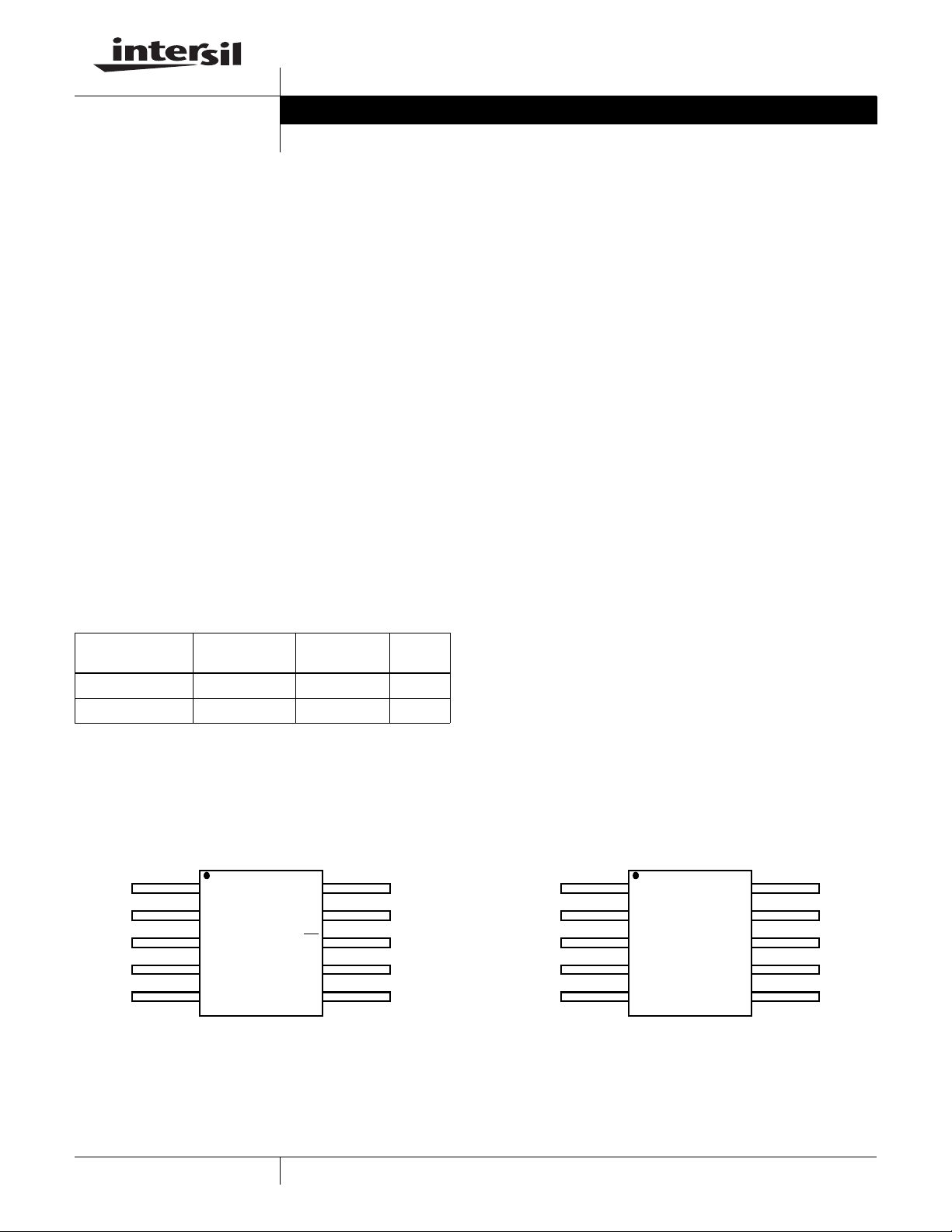
5962-0625601QXC
(10 LD FLAT PACK)
TOP VIEW
1
NC
2
IN-
3
IN+
4
VS-
5
NC
NC
NC
CE
VS+
OUT
10
9
8
7
6
5962-0625602QXC
(10 LD FLAT PACK)
TOP VIEW
1
NC
2
IN-
3
IN+
4
VS-
5
NC
NC
NC
NC
VS+
OUT
10
9
8
7
6
1
CAUTION: These devices are sensitive to electrostatic discharge; follow proper IC Handling Procedures.
1-888-INTERSIL or 1-888-468-3774
| Intersil (and design) is a registered trademark of Intersil Americas Inc.
All other trademarks mentioned are the property of their respective owners.
Copyright Intersil Americas Inc. 2007. All Rights Reserved
5962-0625601QXC, 5962-0625602QXC
www.BDTIC.com/Intersil
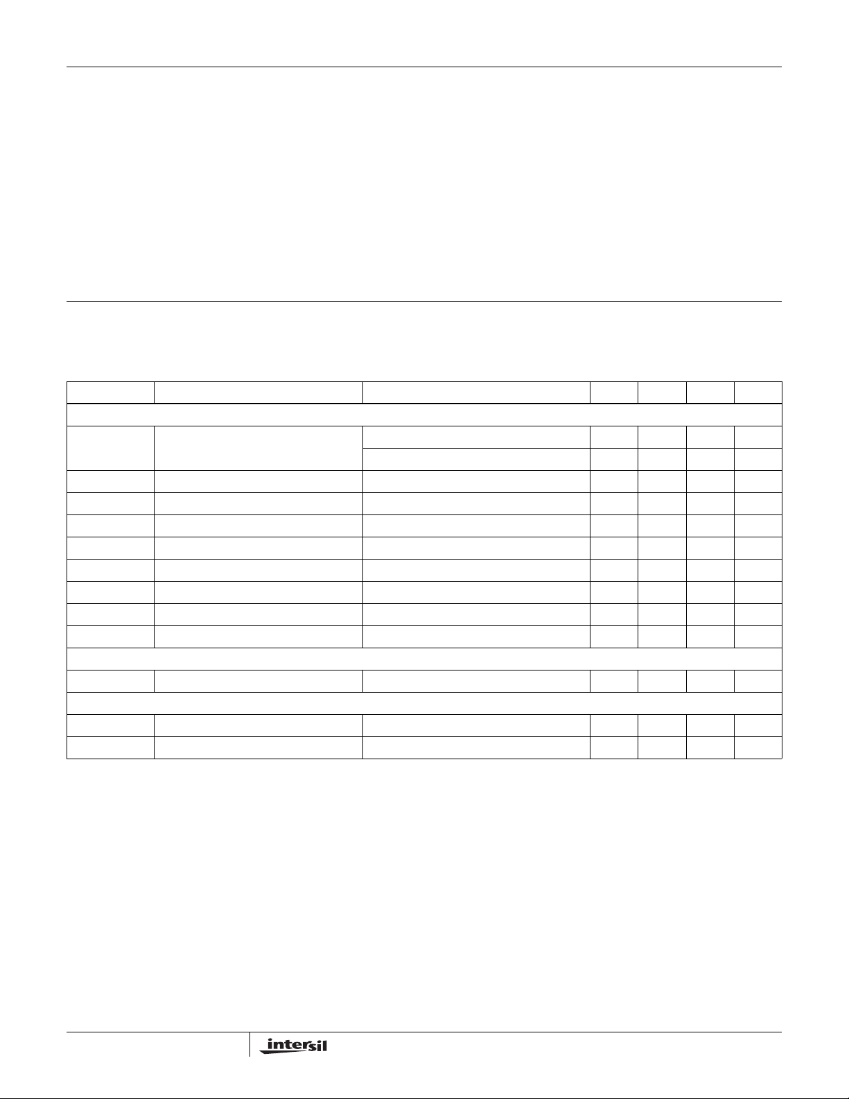
Absolute Maximum Ratings (T
Supply Voltage between VS+ and VS-. . . . . . . . . . . . . . . . . . . 12.6V
Slewrate between V
Maximum Continuous Output Current . . . . . . . . . . . . . . . . . . . 20mA
I into V
Pin Voltages. . . . . . . . . . . . . . . . . . . . . . . . . V
CAUTION: Do not operate at or near the maximum ratings listed for extended periods of time. Exposure to such conditions may adversely impact product reliability and
result in failures not covered by warranty.
NOTES:
IMPORTANT NOTE: All parameters having Min/Max specifications are guaranteed. Typical values are for information purposes only. Unless otherwise noted, all tests
are at the specified temperature and are pulsed tests, therefore: T
+, VIN-, Enable Pins . . . . . . . . . . . . . . . . . . . . . . . . . ±4mA
IN
1. θ
is measured with the component mounted on a low effective thermal conductivity test board in free air. See Tech Brief TB379 for details.
JA
2. For θ
, the “case temp” location is the center of the exposed metal pad on the package underside.
JC
+ and VS-. . . . . . . . . . . . . . . . . . . . . . . . 1V/µs
S
Electrical Specifications V
PARAMETER DESCRIPTION CONDITIONS MIN TYP MAX UNIT
AC PERFORMANCE
BW -3dB Bandwidth A
BW1 0.1dB Bandwidth AV = +2 100 MHz
SR Slew Rate V
t
S
e
N
- IN- Input Current Noise 19 pA/√Hz
i
N
+ IN+ Input Current Noise 50 pA/√Hz
i
N
dG Differential Gain Error (Note 3) AV = +2 0.01 %
dP Differential Phase Error (Note 3) A
INPUT CHARACTERISTICS
C
IN
ENABLE (5962-0625601QXC ONLY)
t
EN
t
DIS
NOTE:
3. Standard NTSC test, AC signal amplitude = 286mV, f = 3.58MHz.
0.1% Settling Time V
Input Voltage Noise 1.7 nV/√Hz
Input Capacitance 1.5 pF
Enable Time 170 ns
Disable Time 1.25 µs
= +25°C) Thermal Information
A
Thermal Resistance (Typical) θ
Flat Pack Package (Notes 1, 2) . . . . . . 165 60
Storage Temperature. . . . . . . . . . . . . . . . . . . . . . . .-65°C to +150°C
- -0.5V to VS+ +0.5V
S
= TC = T
J
+ = +5V, VS- = -5V, RF = 392Ω for AV = 1, RF = 250Ω for AV = 2, RL = 150Ω, TA = +25°C
S
Unless Otherwise Specified.
A
= +1 1400 MHz
V
= +2 800 MHz
A
V
= -2.5V to +2.5V, AV = +2 6000 V/µs
O
= -2.5V to +2.5V, AV = -1 8 ns
OUT
= +2 0.03 °
V
Ambient Operating Temperature . . . . . . . . . . . . . . .-55°C to +125°C
Die Junction Temperature . . . . . . . . . . . . . . . . . . . . . . . . . . . +150°C
Power Dissipation . . . . . . . . . . . . . . . . . . . . . . . . . . . . . . . . .144mW
(°C/W) θJC (°C/W)
JA
2
FN6491.1
October 17, 2007

Pin Descriptions
V
V
www.BDTIC.com/Intersil
5962-0625601QXC, 5962-0625602QXC
5962-0625601QXCIS
(10 Ld FLAT PACK)
1, 5, 9, 10 1, 5, 8 , 9 ,10 NC Not connected
2 2 IN- Inverting input
3 3 IN+ Non-inverting input (See circuit 1)
4 4 VS- Negative supply
6 6 OUT Output
7 7 VS+ Positive supply
8CE
5962-0625602QXCIS
(10 ld FLAT PACK) Pin Name Function Equivalent Circuit
Chip enable
CIRCUIT 1
CIRCUIT 2
VS+
OUT
V
S
+
S
IN-IN+
V
-
S
-
+
S
CE
V
-
S
CIRCUIT 3
All Intersil U.S. products are manufactured, assembled and tested utilizing ISO9000 quality systems.
Intersil Corporation’s quality certifications can be viewed at www.intersil.com/design/quality
Intersil products are sold by description only. Intersil Corporation reserves the right to make changes in circuit design, software and/or specifications at any time without
notice. Accordingly, the reader is cautioned to verify that data sheets are current before placing orders. Information furnished by Intersil is believed to be accurate and
reliable. However, no responsibility is assumed by Intersil or its subsidiaries for its use; nor for any infringements of patents or other rights of third parties which may result
from its use. No license is granted by implic atio n or other wise u nde r any p a tent or patent rights of Intersil or its subsidiaries.
For information regarding Intersil Corporation and its products, see www.intersil.com
3
FN6491.1
October 17, 2007

5962-0625601QXC, 5962-0625602QXC
www.BDTIC.com/Intersil
Ceramic Metal Seal Flatpack Packages (Flatpack)
e
-A- -B-
b
0.004 H A - BMD
Q
A
-C-
SEATING AND
BASE PLANE
L
c1
M
PIN NO. 1
ID AREA
E1
S S
E
E3 E3
LEAD FINISH
BASE
METAL
b1
M
(b)
SECTION A-A
0.036 H A - BMD
-D-
LE2
(c)
NOTES:
1. Index area: A notch or a pin one identification mark shall be located adjacent to pin one and shall be located within the shaded
area shown. The manufacturer’s identification shall not be used
as a pin one identification mark. Alternately, a tab (dimension k)
may be used to identify pin one.
2. If a pin one identification mark is used in addition to a tab, the limits of dimension k do not apply.
3. This dimension allows for off-center lid, meniscus, and glass
overrun.
4. Dimensions b1 and c1 apply to lead base metal only. Dimension
M applies to lead plating and finish thickness. The maximum limits of lead dimensions b and c or M shall be measured at the centroid of the finished lead surfaces, when solder dip or tin plate
lead finish is applied.
5. N is the maximum number of terminal positions.
6. Measure dimension S1 at all four corners.
7. For bottom-brazed lead packages, no organic or polymeric materials shall be molded to the bottom of the package to cover the
leads.
8. Dimension Q shall be measured at the point of exit (beyond the
meniscus) of the lead from the body. Dimension Q minimum
shall be reduced by 0.0015 inch (0.038mm) maximum when solder dip lead finish is applied.
9. Dimensioning and tolerancing per ANSI Y14.5M - 1982.
10. Controlling dimension: INCH.
S1
S S
C
A
A
D
-H-
K10.A MIL-STD-1835 CDFP3-F10 (F-4A, CONFIGURATION B)
10 LEAD CERAMIC METAL SEAL FLATPACK PACKAGE
INCHES MILLIMETERS
SYMBOL
A 0.045 0.115 1.14 2.92 -
b 0.015 0.022 0.38 0.56 -
b1 0.015 0.019 0.38 0.48 -
c 0.004 0.009 0.10 0.23 -
c1 0.004 0.006 0.10 0.15 -
D - 0.290 - 7.37 3
E 0.240 0.260 6.10 6.60 -
E1 -0.280-7.113
E2 0.125 - 3.18 - -
E3 0.030 - 0.76 - 7
e 0.050 BSC 1.27 BSC -
k 0.008 0.015 0.20 0.38 2
L 0.250 0.370 6.35 9.40 -
Q 0.026 0.045 0.66 1.14 8
S1 0.005 - 0.13 - 6
M - 0.0015 - 0.04 -
N10 10-
NOTESMIN MAX MIN MAX
Rev. 0 3/07
4
FN6491.1
October 17, 2007
 Loading...