

®
5962-0623601QPC, 5962-0623602QPC
Data Sheet March 28, 2007
670MHz Low Noise Amplifiers
The 5962-0623601QPC and 5962-0623602QPC are fully
DSCC SMD compliant parts and the SMD data sheets are
available on the DSCC website (http://www.dscc.dla.mil/
programs/specfind/default.asp). The 5962-0623601QPC is
electrically equivalent to the EL5132 and the
5962-0623602QPC is electrically equivalent to the EL5133,
reference these data sheets for additional information.
These amplifiers are ultra-low voltage noise, high speed,
low power consumption voltage feedback amplifiers.
Both amplifiers are stable at gains as low as 10. Not only do
these devices find perfect application in high gain
applications, they maintain their performance down to lower
gain settings.
These amplifiers are available in SBDIP packages. All parts
are specified for operation over the -55°C to +125°C
temperature range.
Ordering Information
PKG.
PART
NUMBER
5962-0623601QPC 5962-0623
5962-0623602QPC 5962-0623
PART
MARKING TEMP (°C) PACKAGE
601QPC
602QPC
-55 to +125 8 Ld SBDIP D8.3
-55 to +125 8 Ld SBDIP D8.3
DWG.
#
FN6473.0
Features
• 670MHz -3dB bandwidth
• Ultra low noise 0.9nV/√Hz
• 1000V/µs slew rate
• Low supply current = 16mA
• Single supplies from 5V to 12V
• Dual supplies from ±2.5V to ±6V
• Fast disable on the 5962-0623601QPC
Applications
• Pre-amplifier
• Receiver
• Filter
• IF and baseband amplifier
• ADC drivers
• DAC buffers
• Instrumentation
• Communications devices.
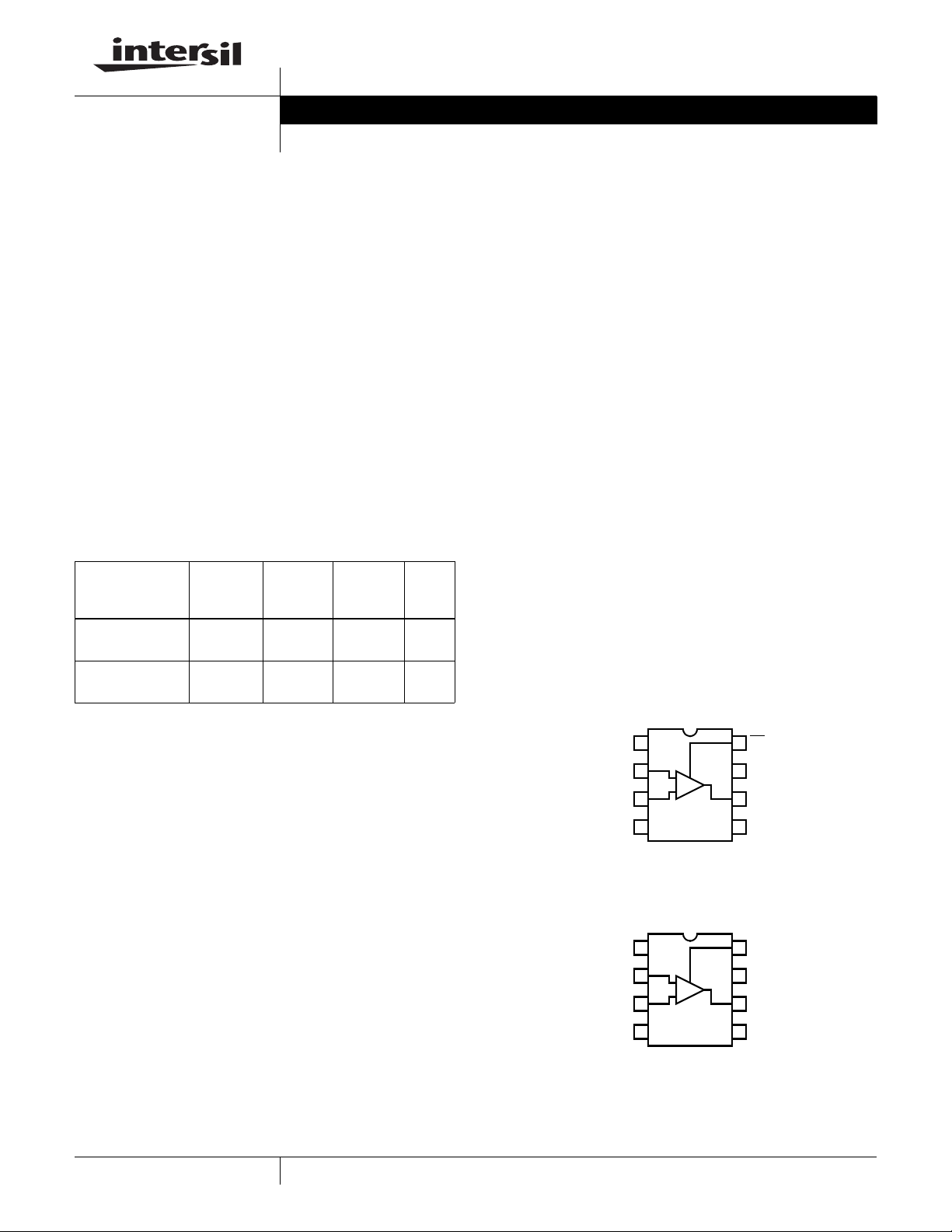
Pinouts
5962-0623601QPC
(8 LD SBDIP)
TOP VIEW
1
NC
IN-
2
-
IN+
VS-
NC
IN-
IN+
VS-
1
CAUTION: These devices are sensitive to electrostatic discharge; follow proper IC Handling Procedures.
1-888-INTERSIL or 1-888-468-3774
| Intersil (and design) is a registered trademark of Intersil Americas Inc.
All other trademarks mentioned are the property of their respective owners.
Copyright Intersil Americas Inc. 2007. All Rights Reserved
+
3
4
5962-0623602QPC
(8 LD SBDIP)
TOP VIEW
1
2
-
+
3
4
8
CE
7
VS+
OUT
6
NC
5
8
NC
VS+
7
OUT
6
NC
5
5962-0623601QPC, 5962-0623602QPC
Absolute Maximum Ratings (T
Supply Voltage from VS+ to VS- . . . . . . . . . . . . . . . . . . . . . . . 13.2V
Slewrate between V
I
-, IIN+, CE . . . . . . . . . . . . . . . . . . . . . . . . . . . . . . . . . . . . . . ±5mA
IN
+ and VS-. . . . . . . . . . . . . . . . . . . . . . . . 1V/µs
S
Continuous Output Current . . . . . . . . . . . . . . . . . . . . . . . . . . . 20mA
CAUTION: Stresses above those listed in “Absolute Maximum Ratings” may cause permanent damage to the device. This is a stress only rating and operation of the
device at these or any other conditions above those indicated in the operational sections of this specification is not implied.
IMPORTANT NOTE: All parameters having Min/Max specifications are guaranteed. Typical values are for information purposes only. Unless otherwise noted, all tests
are at the specified temperature and are pulsed tests, therefore: TJ = TC = T
Electrical Specifications V
= +25°C) Thermal Information
A
Storage Temperature. . . . . . . . . . . . . . . . . . . . . . . .-65°C to +150°C
Ambient Operating Temperature . . . . . . . . . . . . . . .-55°C to +125°C
Operating Junction Temperature . . . . . . . . . . . . . . . . . . . . . . +150°C
Power Dissipation . . . . . . . . . . . . . . . . . . . . . . . . . . . . . . . . .192mW
A
+ = +5V, VS- = -5V, RL = 500Ω, RF = 10kΩ, RG = 100Ω, TA = +25°C, unless otherwise specified.
S
PARAMETER DESCRIPTION CONDITIONS MIN TYP MAX UNIT
R
IN
C
IN
BW -3dB Bandwidth R
BW ±0.1dB Bandwidth R
Input Resistance Common mode 5 MΩ
Input Capacitance 2pF
= 225Ω, AV = +10, RL = 1kΩ 670 MHz
F
= 225Ω, AV = +10, RL = 1kΩ 90 MHz
F
GBWP Gain Bandwidth Product 3000 MHz
PM Phase Margin R
SR Slew Rate R
t
, t
R
F
Rise Time, Fall Time ±0.1V
OS Overshoot ±0.1V
t
S
0.01% Settling Time 6.6 ns
dG Differential Gain R
dP Differential Phase RF = 1kΩ, R
e
N
i
N
Input Noise Voltage f = 10kHz 0.9 nV/√Hz
Input Noise Current f = 10kHz 3.5 pA/√Hz
= 1kΩ, CL = 6pF 55 °
L
= 100Ω, V
L
STEP
STEP
= 1kΩ, R
F
= ±2.5V 1000 V/µs
OUT
2.0 ns
10 %
= 150Ω 0.01 %
LOAD
= 150Ω 0.01 °
LOAD
ENABLE (5962-0623601QPC Only)
t
t
EN
DIS
Enable Time 220 nS
Disable Time 175 nS
Pin Descriptions
1, 5 1, 5, 8 NC Not connected
2 2 IN- Inverting input
3 3 IN+ Non-inverting input
4 4 VS- Negative power supply
6 6 OUT Amplifier output
7 7 VS+ Positive power supply
8CE
PART
PIN NAME FUNCTION5962-0623601QPC 5962-0623602QPC
Enable and disable input
2
FN6473.0
March 28, 2007

5962-0623601QPC, 5962-0623602QPC
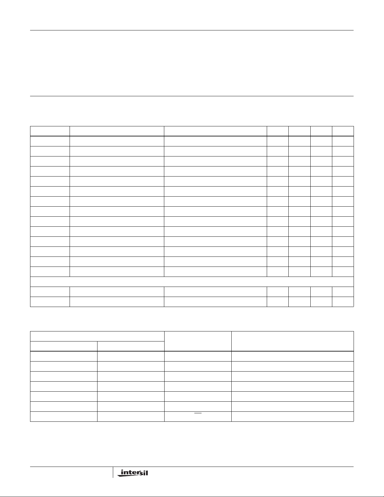
Ceramic Dual-In-Line Metal Seal Packages (SBDIP)
c1
LEAD FINISH
-A-
-B-
S
bbb C A - B
BASE
PLANE
SEATING
PLANE
S1
b2
ccc
b
CA - BM
D
A
A
e
DS S
NOTES:
1. Index area: A notch or a pin one identification mark shall be located adjacent to pin one and shall be located within the shaded
area shown. The manufacturer’s identification shall not be used
as a pin one identification mark.
2. The maximum limits of lead dimensions b and c or M shall be
measured at the centroid of the finished lead surfaces, when
solder dip or tin plate lead finish is applied.
3. Dimensions b1 and c1 apply to lead base metal only. Dimension
M applies to lead plating and finish thickness.
4. Corner leads (1, N, N/2, and N/2+1) may be configured with a
partial lead paddle. For this configuration dimension b3 replaces
dimension b2.
5. Dimension Q shall be measured from the seating plane to the
base plane.
6. Measure dimension S1 at all four corners.
7. Measure dimension S2 from the top of the ceramic body to the
nearest metallization or lead.
8. N is the maximum number of terminal positions.
9. Braze fillets shall be concave.
10. Dimensioning and tolerancing per ANSI Y14.5M - 1982.
11. Controlling dimension: INCH.
-D-
BASE
E
S
S
D
Q
S2
-C-
METAL
b1
M
(b)
SECTION A-A
A
L
(c)
M
eA
aaa
eA/2
CA - BM DS S
c
D8.3 MIL-STD-1835 CDIP2-T8 (D-4, CONFIGURATION C)
8 LEAD CERAMIC DUAL-IN-LINE METAL SEAL PACKAGE
INCHES MILLIMETERS
SYMBOL
A - 0.200 - 5.08 -
b 0.014 0.026 0.36 0.66 2
b1 0.014 0.023 0.36 0.58 3
b2 0.045 0.065 1.14 1.65 -
b3 0.023 0.045 0.58 1.14 4
c 0.008 0.018 0.20 0.46 2
c1 0.008 0.015 0.20 0.38 3
D - 0.405 - 10.29 -
E 0.220 0.310 5.59 7.87 -
e 0.100 BSC 2.54 BSC -
eA 0.300 BSC 7.62 BSC -
eA/2 0.150 BSC 3.81 BSC -
L 0.125 0.200 3.18 5.08 -
Q 0.015 0.060 0.38 1.52 5
S1 0.005 - 0.13 - 6
S2 0.005 - 0.13 - 7
o
α
90
105
o
90
o
105
aaa - 0.015 - 0.38 -
bbb - 0.030 - 0.76 -
ccc - 0.010 - 0.25 -
M - 0.0015 - 0.038 2
N8 88
NOTESMIN MAX MIN MAX
o
Rev. 0 4/94
-
All Intersil U.S. products are manufactured, assembled and tested utilizing ISO9000 quality systems.
Intersil Corporation’s quality certifications can be viewed at www.intersil.com/design/quality
Intersil products are sold by description only. Intersil Corporation reserves the right to make changes in circuit design, software and/or specifications at any time without
notice. Accordingly, the reader is cautioned to verify that data sheets are current before placing orders. Information furnished by Intersil is believed to be accurate and
reliable. However, no responsibility is assumed by Intersil or its subsidiaries for its use; nor for any infringements of patents or other rights of third parties which may result
from its use. No license is granted by implicat ion or oth erwise u nde r any p a tent or p at ent r ights of Intersil or its subsidiari es.
For information regarding Intersil Corporation and its products, see www.intersil.com
3
FN6473.0
March 28, 2007
 Loading...