

Datasheet 5962-0620705Q3A, 5962-0620706Q3A, 5962-0620707Q2A, 5962-0620708Q2A Datasheet (intersil)
®
http://www.BDTIC.com/Intersil
5962-0620705Q3A, 5962-0620706Q3A,
5962-0620707Q2A, 5962-0620708Q2A
Data Sheet May 31, 2006
±15kV ESD Protected, +5.0V 1Microamp,
250kbps, RS-232 Transmitters/Receivers
The Intersil 5962-062070xQxA devices are 5.0V powered
RS-232 transmitters/receivers which meet ElA/TIA-232 and
V.28/V.24 specifications. Additionally, they provide ±15kV
ESD protection (IEC61000-4-2 Air Gap and MIL-STD 883
Human Body Model) on transmitter outputs and receiver
inputs (RS-232 pins). Targeted applications include
ruggedized portable products and remotely deployed
devices exposed to extreme temperature and humidity
where the low operational and even lower standby, power
consumption is critical. Efficient on-chip charge pumps,
coupled with manual and automatic power-down functions
(except for the 5962-0620707Q2A), reduce the standby
supply current to a 1µA trickle. Small footprint packaging and
the use of small, low value capacitors ensure board space
savings as well. Data rates greater than 250kbps are
guaranteed at worst case load conditions. This family is fully
compatible with 5.0V-only systems.
Specifications for QML devices are controlled by the
Defense Supply Center in Columbus (DSCC). The SMD
numbers listed here must be used when ordering.
Detailed Electrical Specifications for these devices are
contained in SMD 5962-06207. A “hot-link” is provided
on our website for downloading.
FN6298.0
Features
• Meets EIA/TIA-232 and V.28/V.24 Specifications at 5V
• Electrically Screened to DSCC SMD#5962-06207
• QML Qualified per MIL-PRF-38535 Requirements
• SMD Compliance
• Military Temperature Range
• Latch-up Free
• Hermetic Package
• ESD Protection for RS-232 I/O Pins to ±15kV (IEC61000)
• Guaranteed Mouse Driveability (ICL3243E)
• Requires Single +5.0V ±10% Power Supply
• Receiver Hysteresis for Improved Noise Immunity
• Low Power Automatic Power-down Modes
(Except for ICL3232E) . . . . . . . . . . . . . . . . . . . . . . . . .1µA
• Guaranteed Minimum 250kbps Data Rate
• Manual and Automatic Power-down Features
• Multiple Drivers/Receivers
• On-Chip Voltage Converters Require Only Four External
Capacitors
• Regulated Dual Charge Pumps
Ordering Information
DESC P/N CONFIGURATION TEMP (°C) PACKAGE
5962-0620705Q3A ICL3243E 3D/5R -55 to +125 28 Ld CLCC
5962-0620706Q3A ICL3238E 5D/3R -55 to +125 28 Ld CLCC
5962-0620707Q2A ICL3232E 2D/2R -55 to +125 20 Ld CLCC
5962-0620708Q2A ICL3221E 1D/1R -55 to +125 20 Ld CLCC
Applications
• Any Military or High-Rel System Requiring RS-232
Communication Ports
- Battery Powered, Hand-Held, and Portable Equipment
- Ruggedized Handheld GPS, Laptop Computers,
Notebooks, Palmtops
- Industrial Control/Shop Floor Communications
- Field Deployed Sensors/Devices Exposed to Extreme
Temperature/Humidity
- Ruggedized Cellular/Mobile Phones
1
CAUTION: These devices are sensitive to electrostatic discharge; follow proper IC Handling Procedures.
1-888-INTERSIL or 1-888-468-3774
| Intersil (and design) is a registered trademark of Intersil Americas Inc.
All other trademarks mentioned are the property of their respective owners.
Copyright Intersil Americas Inc. 2006. All Rights Reserved
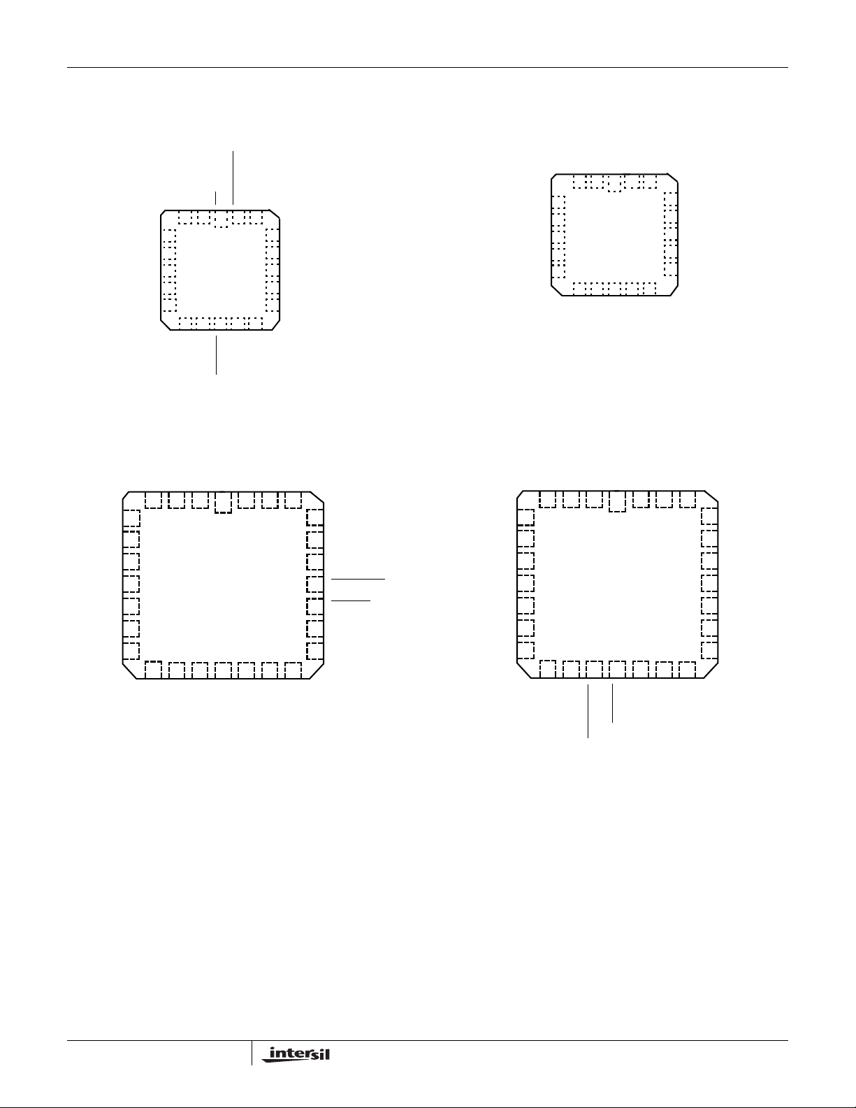
Pinouts
http://www.BDTIC.com/Intersil
5962-0620705Q3A, 5962-0620706Q3A, 5962-0620707Q2A, 5962-0620708Q2A
C1-
C2+
C2-
NC
4
5
6
V-
7
8
ICL3221E (CLCC)
TOP VIEW
EN
C1+
V+
3
9101112
IN
R1
FORCEOFF
220119
13
IN
OUT
T1
R1
INVALID
VCC
18
17
16
15
14
NC
NC
GND
T1OUT
NC
FORCEON
C1-
C2+
C2-
NC
4
5
6
V-
7
8
ICL3232E (CLCC)
TOP VIEW
C1+
V+
VCC
R2
GND
13
IN
NC
OUT
T2
NC
3
220119
9101112
IN
OUT
R2
T2
NC
18
T1
17
OUT
R1
16
IN
R1
15
OUT
14
T1
IN
T
T
T
R
2 IN
R
3 IN
R
4 IN
R
5 IN
1 OUT
2 OUT
3 OUT
5
6
7
8
9
10
11
ICL3243E (CLCC)
1 IN
R
V-
3 2 14
14 15 16 17 1812 13
3 INT2 INT1 IN
T
TOP VIEW
C2+
C2-
5 OUT
R
+
1
V+
C
28 27 26
4 OUTR3 OUTR2 OUT
R
VCC
25
24
23
22
21
20
19
GND
C1-
FORCEON
FORCEOFF
INVALID
R
2OUTB
R
1 OUT
T1 OUT
T2 OUT
T3 OUT
R1 IN
R2 IN
T4 OUT
R3 IN
ICL3238E (CLCC)
TOP VIEW
V-
5
6
7
8
9
10
11
T5 OUT
GND
C2-
3 2 14
14 15 16 17 1812 13
FORCEON
FORCEOFF
C1+
C2+
28 27 26
INVALID
R1OUTB
V+
T5 IN
VCC
25
24
23
22
21
20
19
R3 OUT
C1-
T1 IN
T2 IN
T3 IN
R1 OUT
R2 OUT
T4 IN
2
FN6298.0
May 31, 2006
5962-0620705Q3A, 5962-0620706Q3A, 5962-0620707Q2A, 5962-0620708Q2A
http://www.BDTIC.com/Intersil
Pin Descriptions
PIN FUNCTION
V
CC
V+ Internally generated positive transmitter supply.
V- Internally generated negative transmitter supply.
GND Ground connection.
C1+ External capacitor (voltage doubler) is connected to this lead.
C1- External capacitor (voltage doubler) is connected to this lead.
C2+ External capacitor (voltage inverter) is connected to this lead.
C2- External capacitor (voltage inverter) is connected to this lead.
T
IN
T
OUT
R
IN
R
OUT
R
OUTB
INVALID
EN
FORCEOFF
System power supply input (4.5V to 5.5V).
TTL/CMOS compatible transmitter Inputs. (Note 1)
±15kV ESD Protected, RS-232 level (nominally ±5.5V) transmitter outputs.
±15kV ESD Protected, RS-232 compatible receiver inputs.
TTL/CMOS level receiver outputs.
TTL/CMOS level, noninverting, always enabled receiver outputs.
Active low output that indicates if no valid RS-232 levels are present on any receiver input.
Active low receiver enable control.
Active low control to shut down transmitters and on-chip power supply. This overrides any automatic circuitry and FORCEON
(See Tables 1 & 2, Note 1).
FORCEON Active high input to override automatic power-down circuitry thereby keeping transmitters active. (FORCEOFF
Note 1).
NOTE:
1. The ICL3238E input pins incorporate positive feedback resistors. Once the input is driven to a valid logic level, the feedback resistor maintains
that logic level until V
RCVR OR
XMTR
EDGE
WITHIN 30
SEC?
ICL3238E
No H H Active Active Active No L Normal Operation (Enhanced
No H H Active Active Active Yes H
Yes H L Active Active Active No L Normal Operation (Enhanced
Yes H L Active Active Active Yes H
No H L High-Z Active Active No L Power-down Due to Enhanced
No H L High-Z Active Active Yes H
FORCEOFF
INPUT
is removed. Unused transmitter inputs may be left unconnected by the user.
CC
TABLE 1. POWER-DOWN LOGIC TRUTH TABLE
RS-232
LEVEL
PRESENT
FORCEON
INPUT
TRANSMITTER
OUTPUTS
RECEIVER
OUTPUTS
R
OUTB
OUTPUT
AT
RECEIVER
INPUT?
INVALID
OUTPUT MODE OF OPERATION
Auto Power-down Disabled)
Auto Power-down Enabled)
Auto Power-down Logic
must be high,
X L X High-Z High-Z Active No L Manual Power-down
X L X High-Z High-Z Active Yes H
3
FN6298.0
May 31, 2006

5962-0620705Q3A, 5962-0620706Q3A, 5962-0620707Q2A, 5962-0620708Q2A
http://www.BDTIC.com/Intersil
TABLE 1. POWER-DOWN LOGIC TRUTH TABLE (Continued)
RS-232
RCVR OR
XMTR
EDGE
WITHIN 30
SEC?
INVALID DRIVING FORCEON AND FORCEOFF (EMULATES AUTOMATIC POWER-DOWN)
X Note 2 Note 2 Active Active Active Yes H Normal Operation
X Note 2 Note 2 High-Z High-Z Active No L Forced Auto Power-down
NOTE:
2. Input is connected to INVALID
RS-232
SIGNAL
PRESENT
AT
RECEIVER
INPUT?
ICL3221E
No H H L Active Active N.A. L Normal Operation
No H H H Active High-Z N.A. L
Yes H L L Active Active N.A. H Normal Operation
Yes H L H Active High-Z N.A. H
No H L L High-Z Active N.A. L Power-down Due to Auto Power-down
No H L H High-Z High-Z N.A. L
Yes L X L High-Z Active N.A. H Manual Power-down
Yes L X H High-Z High-Z N.A. H Manual Power-down w/Rcvr. Disabled
No L X L High-Z Active N.A. L Manual Power-down
No L X H High-Z High-Z N.A. L Manual Power-down w/Rcvr. Disabled
ICL3243E
No H H N.A. Active Active Active L Normal Operation
Yes H L N.A. Active Active Active H Normal Operation
No H L N.A. High-Z Active Active L Power-down Due to Auto Power-down
Yes L X N.A. High-Z High-Z Active H Manual Power-down
No L X N.A. High-Z High-Z Active L Manual Power-down
NOTE:
3. Applies only to the ICL3243E.
FORCEOFF
INPUT
FORCEOFF
INPUT
FORCEON
INPUT
Output.
TABLE 2. POWER-DOWN AND ENABLE LOGIC TRUTH TABLE
FORCEON
INPUTENINPUT
TRANSMITTER
OUTPUTS
TRANSMITTER
OUTPUTS
RECEIVER
OUTPUTS
RECEIVER
OUTPUTS
R
OUTB
OUTPUT
LEVEL
PRESENT
RECEIVER
INPUT?
(NOTE 3)
R
OUTB
OUTPUTS
AT
INVALID
OUTPUT MODE OF OPERATION
INVALID
OUTPUT MODE OF OPERATION
(Auto Power-down Disabled)
(Auto Power-down Enabled)
Logic
(Auto Power-down Disabled)
(Auto Power-down Enabled)
Logic
4
FN6298.0
May 31, 2006

5962-0620705Q3A, 5962-0620706Q3A, 5962-0620707Q2A, 5962-0620708Q2A
http://www.BDTIC.com/Intersil
Absolute Maximum Ratings Thermal Information
VCC to Ground . . . . . . . . . . . . . . . . . . . . . . . . . . . . . . . . -0.3V to 6V
V+ to Ground . . . . . . . . . . . . . . . . . . . . . . . . . . . . . . . . . -0.3V to 7V
V- to Ground . . . . . . . . . . . . . . . . . . . . . . . . . . . . . . . . +0.3V to -7V
V+ to V- . . . . . . . . . . . . . . . . . . . . . . . . . . . . . . . . . . . . . . . . . . . 14V
Input Voltages
, FORCEOFF, FORCEON, EN . . . . . . . . . . . . . . . -0.3V to 6V
T
IN
. . . . . . . . . . . . . . . . . . . . . . . . . . . . . . . . . . . . . . . . . . . . ±25V
R
IN
Output Voltages
. . . . . . . . . . . . . . . . . . . . . . . . . . . . . . . . . . . . . . . . . . ±13.2V
T
OUT
, INVALID. . . . . . . . . . . . . . . . . . . . . . . . -0.3V to VCC +0.3V
R
OUT
Short Circuit Duration
. . . . . . . . . . . . . . . . . . . . . . . . . . . . . . . . . . . . . . Continuous
T
OUT
ESD Rating (Receiver Input and Transmitter Output Pins) . . .±15kV
CAUTION: Stresses above those listed in “Absolute Maximum Ratings” may cause permanent damage to the device. This is a stress only rating and operation of the
device at these or any other conditions above those indicated in the operational sections of this specification is not implied.
Thermal Resistance (Typical)
20 Ld CLCC Package . . . . . . . . . . . . . . . . . . . . . . . 90
28 Ld CLCC Package . . . . . . . . . . . . . . . . . . . . . . . 70
Maximum Junction Temperature (Ceramic Package) . . . . 150°C
Maximum Storage Temperature Range . . . . . . . . . .-65°C to 150°C
Maximum Lead Temperature (Soldering 10s) . . . . . . . . . . . . 300°C
θ
JA
(°C/W)
Operating Conditions
Temperature Range
ICL32XXE . . . . . . . . . . . . . . . . . . . . . . . . . . . . . . .-55°C to 125°C
Electrical Specifications ICL3221E, ICL3232E, ICL3243E Test Conditions: V
Unless Otherwise Specified. Typicals are at T
PARAMETER TEST CONDITIONS
DC CHARACTERISTICS
Supply Current, Automatic
Power-down
Supply Current, Power-down FORCEOFF
Supply Current, Power-up All Outputs Unloaded, FORCEON = FORCEOFF
LOGIC AND TRANSMITTER INPUTS AND RECEIVER OUTPUTS
Input Logic Threshold Low T
Input Logic Threshold High T
Input Leakage Current T
Output Leakage Current
(Except ICL3232E)
Output Voltage Low I
Output Voltage High I
AUTOMATIC POWER-DOWN (ICL3221E, ICL3243E Only, FORCEON = GND, FORCEOFF = V
Receiver Input Thresholds to
Enable Transmitters
Receiver Input Thresholds to
Disable Transmitters
INVALID
INVALID
RECEIVER INPUTS
Input Voltage Range Full -25 - 25 V
Input Threshold Low Full 0.6 1.2 - V
Input Threshold High Full - 1.5 2.4 V
Input Resistance Full 3 5 7 kΩ
TRANSMITTER OUTPUTS
Output Voltage Swing All Transmitter Outputs Loaded with 3kW to Ground Full ±5.0 ±5.4 - V
Output Resistance V
Output Short-Circuit Current Full - ±35 ±60 mA
Output Voltage Low I
Output Voltage High I
Open, FORCEON = GND, FORCEOFF =V
All R
IN
(ICL3221E, ICL3243E Only)
= GND (Except ICL3232E) Full - 1 10 µA
, FORCEON, FORCEOFF, EN Full - - 0.8 V
IN
, FORCEON, FORCEOFF, EN Full 2.2 - - V
IN
, FORCEON, FORCEOFF, EN Full - ±0.01 ±10 µA
IN
FORCEOFF
OUT
OUT
Powers Up Full -2.7 - 2.7 V
Powers Down Full -0.3 - 0.3 V
OUT
OUT
CC
=GND or EN=V
= 1.6mA Full - - 0.4 V
= -1.0mA Full V
= 1.6mA Full - - 0.4 V
= -1.0mA Full VCC-0.9 - - V
= V+ = V- = 0V, Transmitter Output = ±2V Full 300 10M - Ω
CC
= 25°C, VCC = 5.0V
A
= 4.5V to 5.5V, C1 = 0.01mF, C2 - C4 = 0.1mF;
CC
TEMP
(°C) MIN TYP MAX UNITS
CC
=V
CC
Full - 1 10 µA
Full - 0.3 1.8 mA
Full - ±0.05 ±10 µA
CC
-0.9 V
CC
)
-0.3 - V
CC
5
FN6298.0
May 31, 2006
5962-0620705Q3A, 5962-0620706Q3A, 5962-0620707Q2A, 5962-0620708Q2A
http://www.BDTIC.com/Intersil
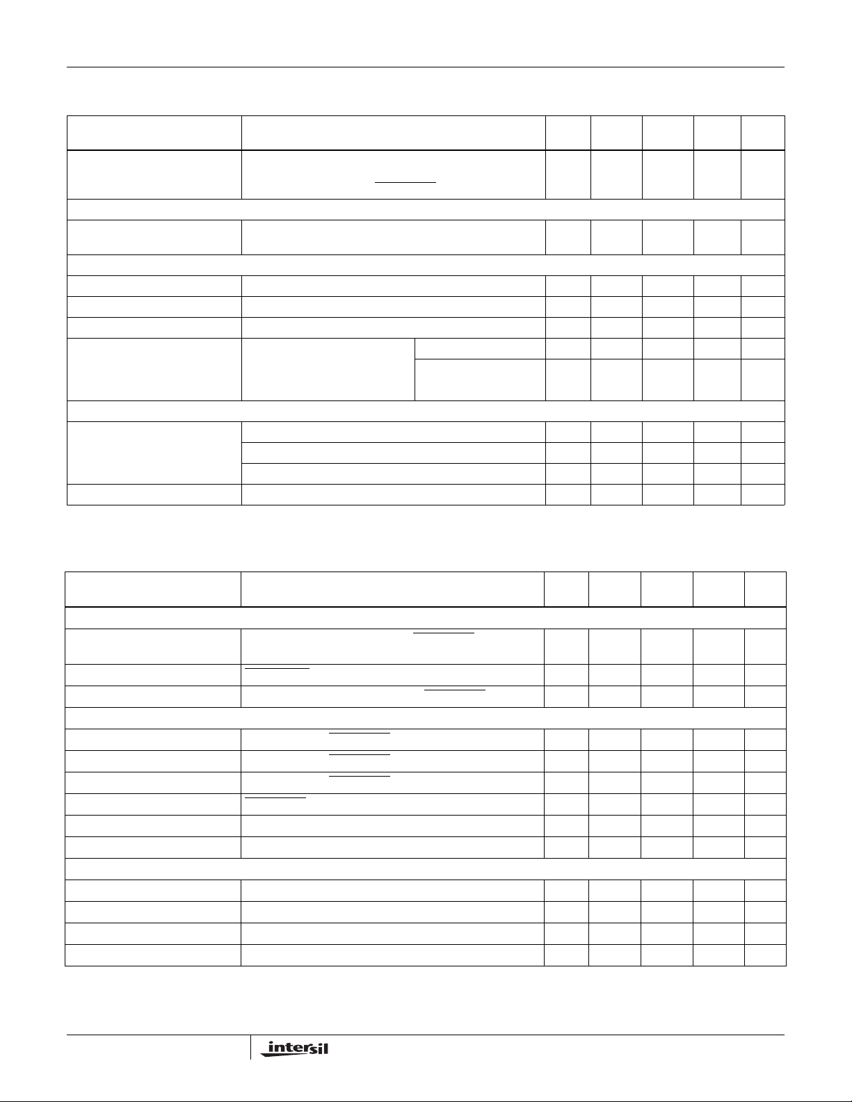
Electrical Specifications ICL3221E, ICL3232E, ICL3243E Test Conditions: V
Unless Otherwise Specified. Typicals are at T
= 25°C, VCC = 5.0V (Continued)
A
= 4.5V to 5.5V, C1 = 0.01mF, C2 - C4 = 0.1mF;
CC
TEMP
PARAMETER TEST CONDITIONS
Output Leakage Current V
=±12V, VCC= 0V or 4.5V to 5.5V
OUT
(ICL3232E,V
Automatic Power-down or FORCEOFF
= 0V only)
CC
=GND
(°C) MIN TYP MAX UNITS
Full - - ±25 µA
MOUSE DRIVEABILITY (ICL3243 Only)
Transmitter Output Voltage T1
GND, T1
=T2IN=GND, T3IN=VCC, T3
IN
OUT
and T2
Loaded with 2.5mA Each
OUT
Loaded with 3kW to
OUT
Full ±5 - - V
TIMING CHARACTERISTICS
Maximum Data Rate R
Transmitter Skew t
Receiver Skew t
Transition Region Slew Rate V
=3kW, CL= 1000pF, One Transmitter Switching Full 250 500 - kbps
L
- t
PHL
PLH
- t
PHL
PLH
=5.0V,
CC
= 3kW to 7kW,
R
L
Measured From 3V to -3V or -3V
= 200pF to 2500pF Full 4 8.0 50 V/µs
C
L
= 200pF to 1000pF Full 6 - 50 V/µs
C
L
Full - 200 1000 ns
Full - 100 1000 ns
to 3V
ESD PERFORMANCE
RS-232 Pins (T
, RIN) Human Body Model (MIL-STD 883 Method 3015) 25 - ±15 - kV
OUT
IEC61000-4-2 Contact Discharge 25 - ±8 - kV
IEC61000-4-2 Air Gap Discharge 25 - ±15 - kV
All Other Pins Human Body Model (MIL-STD 883 Method 3015) 25 - ±2 - kV
Electrical Specifications ICL3238E Test Conditions: V
Typicals are at T
= 25°C, VCC = 5.0V
A
= 4.5V to 5.5V, C1 = 0.01mF, C2 - C4 = 0.1mF, Unless Otherwise Specified.
CC
TEMP
PARAMETER TEST CONDITIONS
(°C) MIN TYP MAX UNITS
DC CHARACTERISTICS
Supply Current, Automatic
Power-down
Supply Current, Power-down FORCEOFF
Supply Current, Power-up All Outputs Unloaded, FORCEON = FORCEOFF
All R
Open, FORCEON = GND, FORCEOFF = V
IN
= GND Full -110µA
CC
= V
CC
Full -110µA
Full -0.31.8mA
LOGIC AND TRANSMITTER INPUTS AND RECEIVER OUTPUTS
Input Logic Threshold Low T
Input Logic Threshold High T
Input Leakage Current T
Output Leakage Current FORCEOFF
Output Voltage Low I
Output Voltage High I
, FORCEON, FORCEOFF Wake up Threshold Full --0.8V
IN
, FORCEON, FORCEOFF Wake up Threshold Full 2.4 - - V
IN
, FORCEON, FORCEOFF, VIN = 0V or VCC (Note 4) Full - ±0.01 ±10 µA
IN
= GND Full - ±0.05 ±10 µA
= 1.0mA Full --0.4V
OUT
= -1.0mA Full V
OUT
CC
-0.9 V
-0.3 - V
CC
RECEIVER INPUTS
Input Voltage Range Full -25 - 25 V
Input Threshold Low Full 0.8 1.5 - V
Input Threshold High Full -1.82.4V
Input Resistance Full 357kΩ
6
FN6298.0
May 31, 2006

5962-0620705Q3A, 5962-0620706Q3A, 5962-0620707Q2A, 5962-0620708Q2A
http://www.BDTIC.com/Intersil
Electrical Specifications ICL3238E Test Conditions: V
Typicals are at T
PARAMETER TEST CONDITIONS
ENHANCED AUTOMATIC POWER-DOWN (FORCEON = GND, FORCEOFF = VCC)
Receiver Input Thresholds to
INVALID
Receiver Input Thresholds to
INVALID
INVALID
INVALID
TRANSMITTER OUTPUTS
Output Voltage Swing All Transmitter Outputs Loaded with 3kΩ to Ground Full ±5.0 ±5.4 - V
Output Short-Circuit Current Full - ±35 ±60 mA
Output Leakage Current V
TIMING CHARACTERISTICS
Maximum Data Rate R
Transmitter Skew t
Receiver Skew t
Transition Region Slew Rate V
ESD PERFORMANCE
RS-232 Pins (T
All Other Pins Human Body Model (MIL-STD 883 Method 3015) 25 - ±2.5 - kV
NOTE:
High
Low
Output Voltage Low I
Output Voltage High I
, RIN) IEC61000-4-2 Air Gap Discharge 25 - ±15 - kV
OUT
4. These inputs utilize a positive feedback resistor. The input current is negligible when the input is at either supply rail.
Powered Up Full -2.7 - 2.7 V
Powered Down Full -0.3 - 0.3 V
= 1.0mA Full - - 0.4 V
OUT
= -1.0mA Full VCC-0.9 - - V
OUT
= ±12V, VCC = 0V or 4.5V to 5.5V,
OUT
Automatic Power-down or FORCEOFF
= 3kΩ, CL = 1000pF, One Transmitter Switching Full 250 500 - kbps
L
- t
PHL
PLH
- t
PHL
PLH
= 5.0V,
CC
= 3kΩ to 7kΩ,
R
L
Measured From 3V to -3V or -3V
to 3V
IEC61000-4-2 Contact Discharge 25 - ±8-kV
Human Body Model (MIL-STD 883 Method 3015) 25 - ±15 - kV
= 25°C, VCC = 5.0V (Continued) (Continued)
A
= 4.5V to 5.5V, C1 = 0.01mF, C2 - C4 = 0.1mF, Unless Otherwise Specified.
CC
TEMP
(°C) MIN TYP MAX UNITS
Full - - ±25 µA
= GND
Full - 200 1000 ns
Full - 100 1000 ns
= 150pF to 1000pF Full 61550V/µs
C
L
= 150pF to 2500pF Full 41250V/µs
C
L
Die Characteristics
INTERFACE MATERIALS:
Glassivation:
Type: PSG (Phosphorous Silicon Glass)
Thickness: 13.0kÅ ± 1.0kÅ
Top Metallization:
Type: AlSiCu
Thickness: 10.0kÅ ± 1kÅ
ASSEMBLY RELATED INFORMATION:
Substrate Potential:
GND
All Intersil U.S. products are manufactured, assembled and tested utilizing ISO9000 quality systems.
Intersil Corporation’s quality certifications can be viewed at www.intersil.com/design/quality
Intersil products are sold by description only. Intersil Corporation reserves the right to make changes in circuit design, software and/or specifications at any time without
notice. Accordingly, the reader is cautioned to verify that data sheets are current before placing orders. Information furnished by Intersil is believed to be accurate and
reliable. However, no responsibility is assumed by Intersil or its subsidiaries for its use; nor for any infringements of patents or other rights of third parties which may result
from its use. No license is granted by implic atio n or other wise u nde r any p a tent or patent rights of Intersil or its subs idi aries.
For information regarding Intersil Corporation and its products, see www.intersil.com
7
ADDITIONAL INFORMATION:
Worst Case Current Density:
5
<2.0 x 10
A/cm
2
Transistor Count:
ICL3221E: 286
ICL3232E: 296
ICL3243E: 464
ICL3238E: 1235
Process:
Si Gate CMOS
FN6298.0
May 31, 2006

5962-0620705Q3A, 5962-0620706Q3A, 5962-0620707Q2A, 5962-0620708Q2A
http://www.BDTIC.com/Intersil
Ceramic Leadless Chip Carrier Packages (CLCC)
j x 45
E1
o
B
h x 45
-E-
E2
e1
o
A
-F-
0.010 E HS S
L
D
D3
0.007 E FM S HS
B1
L2
D1
-H-
D2
B2
J28.A MIL-STD-1835 CQCC1-N28 (C-4)
28 PAD CERAMIC LEADLESS CHIP CARRIER PACKAGE
INCHES MILLIMETERS
SYMBOL
A 0.060 0.100 1.52 2.54 6, 7
A1 0.050 0.088 1.27 2.23 -
B-----
B1 0.022 0.028 0.56 0.71 2, 4
E
E3
0.010 E FSS
A1
PLANE 2
PLANE 1
e
L3
B3
L1
B2 0.072 REF 1.83 REF B3 0.006 0.022 0.15 0.56 -
D 0.442 0.460 11.23 11.68 D1 0.300 BSC 7.62 BSC D2 0.150 BSC 3.81 BSC D3 - 0.460 - 11.68 2
E 0.442 0.460 11.23 11.68 E1 0.300 BSC 7.62 BSC E2 0.150 BSC 3.81 BSC E3 - 0.460 - 11.68 2
e 0.050 BSC 1.27 BSC -
e1 0.015 - 0.38 - 2
h 0.040 REF 1.02 REF 5
j 0.020 REF 0.51 REF 5
L 0.045 0.055 1.14 1.40 -
L1 0.045 0.055 1.14 1.40 L2 0.075 0.095 1.90 2.41 -
L3 0.003 0.015 0.08 0.038 ND 7 7 3
NE 7 7 3
N28 283
NOTES:
1. Metallized castellations shall be connected to plane 1 terminals
and extend toward plane 2 across at least two layers of ceramic
or completely across all of the ceramic layers to make electrical
connection with the optional plane 2 terminals.
2. Unless otherwise specified, a minimum clearance of 0.015 inch
(0.38mm) shall be maintained between all metallized features
(e.g., lid, castellations, terminals, thermal pads, etc.)
3. Symbol “N” is the maximum number of terminals. Symbols “ND”
and “NE” are the number of terminals along the sides of length
“D” and “E”, respectively.
4. The required plane 1 terminals and optional plane 2 terminals (if
used) shall be electrically connected.
5. The corner shape (square, notch, radius, etc.) may vary at the
manufacturer’s option, from that shown on the drawing.
6. Chip carriers shall be constructed of a minimum of two ceramic
layers.
7. Dimension “A” controls the overall package thickness. The maximum “A” dimension is package height before being solder dipped.
8. Dimensioning and tolerancing per ANSI Y14.5M-1982.
9. Controlling dimension: INCH.
NOTESMIN MAX MIN MAX
Rev. 0 5/18/94
8
FN6298.0
May 31, 2006

5962-0620705Q3A, 5962-0620706Q3A, 5962-0620707Q2A, 5962-0620708Q2A
http://www.BDTIC.com/Intersil
Ceramic Leadless Chip Carrier Packages (CLCC)
j x 45
E1
o
B
h x 45
-E-
E2
e1
o
A
-F-
0.010 E HS S
L
D
D3
0.007 E FM S HS
B1
L2
D1
-H-
D2
B2
J20.A MIL-STD-1835 CQCC1-N20 (C-2)
20 PAD CERAMIC LEADLESS CHIP CARRIER PACKAGE
INCHES MILLIMETERS
SYMBOL
A 0.060 0.100 1.52 2.54 6, 7
A1 0.050 0.088 1.27 2.23 -
B-----
B1 0.022 0.028 0.56 0.71 2, 4
E
E3
0.010 E FSS
A1
PLANE 2
PLANE 1
e
L3
B3
L1
B2 0.072 REF 1.83 REF B3 0.006 0.022 0.15 0.56 -
D 0.342 0.358 8.69 9.09 D1 0.200 BSC 5.08 BSC D2 0.100 BSC 2.54 BSC D3 -0.358-9.092
E 0.342 0.358 8.69 9.09 E1 0.200 BSC 5.08 BSC E2 0.100 BSC 2.54 BSC E3 -0.358-9.09 2
e 0.050 BSC 1.27 BSC -
e1 0.015 - 0.38 - 2
h 0.040 REF 1.02 REF 5
j 0.020 REF 0.51 REF 5
L 0.045 0.055 1.14 1.40 -
L1 0.045 0.055 1.14 1.40 L2 0.075 0.095 1.91 2.41 -
L3 0.003 0.015 0.08 0.38 ND 5 5 3
NE 5 5 3
N20 203
NOTES:
1. Metallized castellations shall be connected to plane 1 terminals
and extend toward plane 2 across at least two layers of ceramic
or completely across all of the ceramic layers to make electrical
connection with the optional plane 2 terminals.
2. Unless otherwise specified, a minimum clearance of 0.015 inch
(0.38mm) shall be maintained between all metallized features
(e.g., lid, castellations, terminals, thermal pads, etc.)
3. Symbol “N” is the maximum number of terminals. Symbols “ND”
and “NE” are the number of terminals along the sides of length
“D” and “E”, respectively.
4. The required plane 1 terminals and optional plane 2 terminals (if
used) shall be electrically connected.
5. The corner shape (square, notch, radius, etc.) may vary at the
manufacturer’s option, from that shown on the drawing.
6. Chip carriers shall be constructed of a minimum of two ceramic
layers.
7. Dimension “A” controls the overall package thickness. The maximum “A” dimension is package height before being solder dipped.
8. Dimensioning and tolerancing per ANSI Y14.5M-1982.
9. Controlling dimension: INCH.
NOTESMIN MAX MIN MAX
Rev. 0 5/18/94
9
FN6298.0
May 31, 2006
 Loading...